Numerical and Experimental Analysis of
On-Chip Optical Wireless Links in Presence of
Obstacles
Volume 13, Number 1, February 2021
Badrul Alam
Giovanna Calò
Gaetano Bellanca
Jacopo Nanni
Ali Emre Kaplan
Marina Barbiroli
Franco Fuschini
Paolo Bassi
Jinous Shafiei Dehkordi
Velio Tralli
Vincenzo Petruzzelli
IEEE Photonics Journal
Numerical And Experimental Analysis
Numerical and Experimental Analysis
of On-Chip Optical Wireless Links
in Presence of Obstacles
Badrul Alam ,1Giovanna Calò ,1Gaetano Bellanca,2
Jacopo Nanni ,3Ali Emre Kaplan,3Marina Barbiroli ,3 Franco Fuschini ,3Paolo Bassi,3Jinous Shafiei Dehkordi ,2
Velio Tralli,2and Vincenzo Petruzzelli 1
1Department of Electrical and Information Engineering, Polytechnic of Bari,Via E. Orabona,
70125 Bari, Italy
2Department of Engineering, University of Ferrara, Via Saragat, 44124 Ferrara, Italy 3Department of Electrical, Electronic and Information Engineering, “G. Marconi”, University
of Bologna, Viale Risorgimento, 40136 Bologna, Italy
DOI:10.1109/JPHOT.2020.3046379
This work is licensed under a Creative Commons Attribution 4.0 License. For more information, see https://creativecommons.org/licenses/by/4.0/
Manuscript received December 2, 2020; accepted December 17, 2020. Date of publication December 21, 2020; date of current version January 7, 2021. This work was supported by the Italian Ministry of Education, University and Research in the framework of the PRIN 2015 "Wireless Networks through on-chip Optical Technology–WiNOT" Project 20155EA8BC-PE7. Corresponding author: Badrul Alam (e-mail: [email protected]).
Abstract: In this work, we analyze the effects of the presence of waveguides in a wireless on-chip optical channel, which act as obstacles for the rays composing the propagating signal. The analysis has been performed numerically by using the FDTD method, and the simulation results have been validated by the experimental characterization. This work focuses on the relationship between the received signal and the position of the obstacles on the circuit plane in a multilayered channel made of heterogeneous dielectric cladding. We show how the crossing waveguide perturbates the received power and we provide ad hoc guidelines for the best topological choices allowing to mitigate losses. Moreover, with a good agreement between numerical and experimental results, amounting to a variation of less than 1 dB, we have demonstrated that the effects of this perturbation in real chips can be predicted. The results of this analysis, as well as increasing the level of knowledge of on-chip optical wireless links, allow a better comprehension and control of unbound optical signals within the optical chip environment.
Index Terms: Optical wireless links, optical wireless network on chips, crossing waveguides.
1. Introduction
Evolution of computation technology faces various challenges. The intrinsic limits of metallic wires and the physical limits of scalability hinder in fact the possibility to address the requirements of higher communication complexities of modern NoCs, both in terms of density and bandwidth [1]. With the current trend towards Chip Multi-Processors, this issue becomes more prevalent, and it is evident that a long-term solution requires a paradigm shift [2]. Two popular solutions to this communication bottleneck are represented by wireless NoCs and optical NoCs. Both approaches have been extensively investigated in the last decade, each presenting its own
set of advantages and disadvantages. Optical NoCs have the benefit of large bandwidths, low propagation losses and integrability, although they are limited by their planar nature since the number of crossings between waveguides corresponds to losses and crosstalk [3]–[5]. Although there are efforts for the integration of a 3D interconnection system [6], [7], a stable technological solution is yet to be defined. Wireless NoCs [8], [9] have the benefit of reducing routing complexity of wires, although they involve the use of multiple modules of transceivers, with the related modu-lation/demodulation, power sources for transmitters, and bulky antennas (working at microwaves). Recently, Optical-Wireless-NoCs (OWiNoCs) have been proposed as an approach that combines optical wires with optical wireless links as a mean for intra/inter-chip communication [10]–[13]. Today, research on optical wireless links over long distances stands on established technologies and methods, whereas it is still in early stages at on-chip-scale distances. Chip level optical wireless links are very interesting, since they may enable a variety of applications, such as the inter- and intra-core communications in Chip Multiprocessors (CMP), beam steering and biosensing on chip, and also potentially overcome the limits caused by the planarity of optical circuits, which can simplify architectures and enable higher communication densities [10], [14]–[16].
In principle, the on-chip wireless communication at optical frequencies can combine, at the chip level, the well-known advantages of wireless communications with those pertaining to photonics, relieving at same time the network topological constraints. However, the OWiNoCs still require extensive research and they involve major challenges in the definition of transmission/reception antennas and in the study of the on-chip optical channel.
An important requirement for optical antennas for OWiNoCs is a high gain in the longitudinal direction (on-chip plane). On this frame, two types of antennas have been developed in recent years, the plasmonic and the dielectric ones [10]–[13], [18]–[20], both with their specific traits [20]. Dielectric antennas [10], [20] allow to reach very high gain in the longitudinal direction, between 16–23 dB. As a counterpart, their dimensions are of the order of various wavelengths (e.g.,∼12–15
μm for 1.55 μm wavelength). On the other hand, plasmonic antennas are more compact, since
they require around two wavelengths of size (e.g.,∼3.2 μm for 1.55 μm wavelength) and allow a longitudinal gain around 10 dB [12]. It should also be noted that the gain of plasmonic antennas can be significantly increased by setting them into arrays [18], [19], which is easy, considering their reduced size.
A further important step in the actual implementation of OWiNoC is the in-depth knowledge of the propagation channel characteristics necessary to predict the communication performances and to deduce network design criteria. For this purpose, different approaches are feasible. In [21]–[23], the propagation of the signal within the optical wireless channel was studied numerically by means of the Finite Difference Time Domain (FDTD) and the Ray Tracing (RT) methods. The FDTD allows a full-wave calculation of the electromagnetic fields and, thus, a complete knowl-edge of the electromagnetic behavior of the system. As a counterpart, FDTD requires considerable computational resources, which limit the analysis to the near field, mainly for the evaluation of the antenna gain, and to the study of the propagation over a few hundreds of micrometers. Conversely, RT allows fast results over longer distances with a satisfactory precision, although at the cost of some degree of approximation [21], [22]. The latter approach is then fundamental for the analysis and the design of complex networks and long-distance links.
In previous studies, structures with increasing geometrical complexity have been addressed by considering, initially, simple boundless homogeneous media [10]–[13], [18]–[23]. Then, more real-istic structures based on a homogeneous cladding, with air on top and Silicon layer on bottom, have been considered using both RT and FDTD [21]–[24]. Those studies underlined the dependence of the performance of wireless links on the antenna configuration, on the geometrical parameters of the system and on the materials composing the antennas and the propagation medium.
Actual optical wireless links involve a multilayer structure that comes from the fabrication steps required for the chip realization. The multilayer structure of the chip introduces additional interfaces in the propagation channel. These interfaces, their relative distance (few wavelengths) and the channel length (tens/hundreds of wavelengths) have been shown to have a strong impact on the final received signal, allowing also noticeable increases of the received signal level [23], [24].
IEEE Photonics Journal
Numerical And Experimental Analysis
Fig. 1. (a) Scheme of the wireless system, where a waveguide interrupts the direct line between the receiver and the transmitter. (b) Top view of the system, with the indication of the relevant geometrical parameters. The inset evidences the antenna geometry. (c) Cross section of the chip, cutting through a straight waveguide; the materials and geometrical characteristics of the optical channel are shown, as well as the dimensions of the standard waveguide (inset).
Further investigation of the propagation channel is proposed in this paper to take into account that, in the implementation of on-chip wireless networks, the optical channel can in fact contain also further optical elements, such as crossing waveguides, which act as obstacles for the propagating signal. The knowledge of the behavior of wireless links in presence of an obstacle can allow to define design criteria for optimal placing of crossing waveguides and it opens up new possibilities for the exploration of different network topologies.
In this work, we numerically and experimentally study the effects of the presence of a waveguide transversely placed in a direct line-of-sight wireless link (here referred to as empty wireless channel - EWC). The crossing waveguide acts as an obstacle for the propagating optical signal. In the following, we will refer to the wireless link with crossing waveguide as Single Obstacle Wireless Channel (SOWC). The reported analysis shows both the numerical and the experimental results and it mainly aims at determining the relationship between the received signal and the position of the obstacle. Most of the analysis was numerically performed by using the FDTD method for distances up to 130μm, since it allows to compute the complete scenario without introducing ap-proximations on the geometry. This study is the first step for the definition of topological guidelines for circuit design, which aim to preserve or even improve the optical channel performance.
The paper is organized as follows. In Section 2 the analyzed system is described, whereas the numerical and experimental setups are described in Section 3 and 4. In Section 5, the results of the numerical and experimental SOWC analyses are discussed. Finally, the conclusions are drawn.
2. Description of the On-Chip Optical Wireless System
Fig. 1 shows a scheme of the on-chip wireless link analyzed in this work. It consists of a transmitter and a receiver facing each other, with a crossing waveguide perpendicular to their direct line of sight (Fig. 1(a)).
The transmitting antenna, shown in the inset of Fig. 1(b), is made of an inverse taper fed by a standard Silicon on Insulator (SOI) waveguide, with width w = 380 nm and height h = 220 nm, which allows the propagation of the single fundamental TE mode. The guided mode propagating in the waveguide becomes evanescent in the inverse taper and it is radiated in the surrounding dielectric. Thanks to the taper, the effective refractive index of the propagating mode is gradually adapted to the one of the surrounding cladding, thus guaranteeing a low back-reflection during the
conversion of the wired signal into a wireless one. In order to improve the radiation characteristics of the antenna, the inverse taper is terminated with a straight tip with length 1μm and width 130 nm. The taper antenna radiates mainly in the x direction with a maximum radiation gain of about 16 dB. Moreover, for the reciprocity of the antenna behavior, it can also act as a receiver trans-forming the wireless signal into a guided one. Further details on the radiation properties of the taper antenna are reported in [10], [20]. It is worth underlining that, as discussed in [10], [20], the radiation gain can be improved up to about 20 dB by adding dielectric directors to the taper antenna. However, since the focus of this work is the analysis of the propagation channel in presence of obstacles, we will consider only simple taper antennas, which exhibit a sufficiently high gain and are easier to fabricate.
The main parameters of the analysis reported in this paper are the link distance Ld, which is the distance between the transmitting and the receiving antennas, and the crossing distance Cd, which is the distance between the transmitter and the perpendicular crossing waveguide, as schematized in Fig. 1(b).
Considering that the implementation of wireless links is envisioned to be an extension of the capabilities of present optical networks on chip, for this study we have chosen technological features suitable for integration on standard SOI platform. The multilayer structure of the fabricated and analyzed sample is shown in Fig. 1(c). The circuit layer, i.e., the silicon layer housing the waveguides and the antennas, is situated upon a 3μm thick layer of SiO2 (with refractive index nSiO2 = 1.445 at the wavelength λ = 1.55 μm), which separates it from the bulk silicon layer. The thickness of the bulk Si layer is about 600μm, therefore, in the numerical simulations, it was considered as infinite. The circuit layer is covered with a 300-nm thick layer of BPTEOS (nclad = 1.453) glass, which was deposited to improve adhesion and to avoid strong index contrasts around the taper tip. The BPTEOS layer, which was planarized before deposition of the cladding, has a thickness of 80 nm with respect to the circuit layer and an overall thickness of 300 nm with respect to the SiO2 layer (i.e., the BPTEOS covers the circuit layer filling the etched regions around the waveguides and the antennas). Upon BPTEOS, a dielectric layer made of UV26 (nUV26= 1.526) polymer was deposited with a thickness of 3.78μm. An infinite layer of Air (nair= 1) is present on top of the whole system.
3. Numerical Analysis Settings
The structure shown in Fig. 1 was numerically analyzed by using the three-dimensional Finite Difference Time Domain (3D-FDTD) method [25]. The multilayer shown in Fig. 1(c) was modeled in all the simulations by considering a semi-infinite extension of the top air layer and of the bottom silicon one. Perfectly Matched Layer (PML) boundary conditions were used to limit the calculation domain [25].
The FDTD method, used to solve the Maxwell equations, involves the spatial discretization of the volume under study as well as the temporal discretization of the full-wave electromagnetic fields. To describe with precision the propagation in the multilayer structure, the maximum mesh size was chosen equal to 25 nm× 25 nm × 25 nm and an adaptive mesh refinement was used to describe the dielectric structures. The FDTD method allows to take into account all the linear interactions between the electromagnetic fields and the structures, including the couplings mechanisms from wireless to guided signals, and the matching between different structures. The PML conditions ensure the lack of back-reflection on all the simulation boundaries.
Provided that the time and space discretization is constrained by the FDTD convergence criteria, the simulation of the wireless links proved to be demanding in terms of computational resources and simulation time. In fact, given that the link distance values Ldare much greater than the oper-ating wavelength (λ = 1.55 μm), the simulations required large computation domains. Therefore, in the parametric analysis of the wireless propagation, we have considered a maximum value of the link distance equal to Ld= 130 μm. Moreover, to reduce the meshing requirements, the trenches, which are present in the actual fabricated sample, were not included in the model due to the expected negligible influence on the received signal.
IEEE Photonics Journal
Numerical And Experimental Analysis
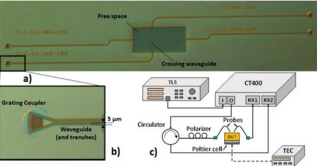
Fig. 2. (a) Optical microscopy image of the fabricated links; in particular, the free space area (corre-sponding to the wireless channel) is shown. (b) Enlargement of a grating coupler, a waveguide and the trenches. (c) Scheme of the experimental setup.
4. Experimental Details
4.1 Fabrication
Fig. 2 shows a microscopy image of the fabricated links with a crossing waveguide. Waveguides, trenches, and wireless propagation area (here, named free-space area), are visible in Fig. 2(a) and (b). In Fig. 2(b) an enlargement of the grating couplers is also shown. The optical structures were patterned through positive resist photolithography followed by etching of a SOI wafer. The resulting sample has trenches, which are distant 5 μm from the waveguides. In the free-space area the wireless links feature a wide opening of the trenches, which is visible on Fig. 2(a). To guarantee a low influence of the rays bouncing on the lateral walls of the free-space area, its width was chosen equal to 0.6∗Ld.
Upon the patterned antenna layer, a 300-nm thick layer of BPTEOS was deposited through Plasma-Enhanced-Chemical-Vapor-Deposition LPCVD. Due to the liquid precursors, this layer is planarized, so its thickness is 80 nm upon the Silicon layer and 300 nm upon the SiO2one. The presence of the BPTEOS, over the SiO2 one, reduces the refractive index discontinuity near the antennas. This is advantageous since such discontinuities can influence the antenna radiation characteristics giving an undesired tilt of the radiation diagram. To cover the BPTEOS layer, a 3.78-μm thick polymeric layer (UV26) was spin-coated and then cured with ultraviolet light and baked at 170 °C.
As shown in Fig. 2(b), gratings are realized for the input/output coupling of the laser signal. Moreover, the waveguide sections include bends that, in addition to grating coupling and trenches, allow the isolation of the signal pertaining to the antennas from other undesired sources of unbound signals.
4.2 Characterization Setup
The experimental setup is shown in Fig. 2(c). A Yenista’s CT400 passive optical component tester, connected and synchronized with a tunable laser source (Yenista’s TLS Tunics T100), has been used to evaluate the ratio between its receiving ports RX1 and RX2 and the power emitted from its output port, returning the transmission and reflection coefficients, respectively.
In detail, the output port of the CT400 is connected first to a circulator, necessary for the evaluation of possible reflections, and then to a polarization controller placed right before the input fiber probe with the purpose of optimizing the coupling between the probe and the fundamental TE mode of the silicon waveguide at the input section of the device under test (DUT).
The fiber probes are vertically coupled to the input and output waveguides of the DUT through the taper grating shown in Fig. 2(b), which allows an easy and repeatable coupling.
The temperature of the device is controlled and stabilized by placing the chip on a Peltier cell, isolated in an aluminum case, connected to an external Thermo Electric Controller (TEC). In order to extrapolate the intrinsic value of the transmission coefficient related to the wireless link only (i.e., removing the losses of external components, connectors and gratings), all the measurements have been normalized with respect to those of a reference waveguide fabricated on the same chip and having the same length of the DUTs (about 2 mm). Finally, the setup presents a minimum detectable transmission coefficient of the wireless links of about−55 dB.
5. Results and Discussions
The wireless propagation in a multi-layer environment is characterized by multi-path phenomena which influence the received power and the efficiency of communication. In [24], the authors experimentally demonstrated the occurrence of multipath phenomena in line-of-sight links without obstacles (i.e., EWC). The need of numerically predicting the channel behavior, for proper and efficient design the wireless links, was also evidenced [24].
Here, we focus on the numerical and experimental study of on-chip wireless links in presence of a single obstacle (SOWC). Actually, in the perspective implementation of wireless on-chip com-munication in combination with wired one, the presence of obstacles (e.g., crossing waveguides) must be considered and their effect must be predicted for the correct placing and connection of the network elements.
To better highlight the influence of the crossing waveguide on the wireless signal propagation we report in Fig. 3 the power density (log10(|Pxyz |)) in the XY plane and in the XZ plane. In particular, Fig. 3(a) and (b) show the power density calculated by FDTD simulations in the XY cutting plane at the circuit level for the EWC and SOWC cases, respectively. The solid lines in Fig. 3 indicate the antenna geometry, whereas the dashed purple line in Fig. 3(b) evidences the position of the crossing waveguide. Similarly, Fig. 3(c) and (d) show the power density calculated in the XZ cutting plane, positioned in the middle of the antennas at Y= 0, for the EWC and SOWC cases, respectively. The dashed black lines correspond to the different layers of the simulated chip, whereas the position of the crossing waveguide is denoted by the purple dot in Fig. 3(d).
We can see in Fig. 3(a) and (c) the presence of zones with high power density and others with low power density, which are induced by the multipath effect in the multilayered chip and correspond to constructive and destructive interference of the rays. In Fig. 3(b) and (d) we notice that the crossing waveguide acts as a perturbation, introducing scattering. It is evident that the single waveguide diffuses away only a limited amount of power, and that the scattered rays cause oscillations due to constructive and destructive interferences. On longer ranges, by comparing Fig. 3(c) and (d) we can infer that the perturbation of the power density distribution is more apparent in the SiO2layer with respect to the BPTEOS and UV26 layers, where the rays incoming to the receiver seem the same as in the EWC case. Moreover, we observed from different simulations that the amount of scattered signal depends on the position of the waveguide in the XY plane (circuit plane).
From Fig. 3(c) and (d), it is also evident that the interfaces between the SiO2, BPTEOS and UV26 layers do not significantly influence the propagation of the wireless signal, thanks to the small index contrast. Conversely, the interfaces at the top and at the bottom layers (i.e., between air and UV26 and between SiO2 and bulk silicon) are responsible of multiple reflection owing to the high index contrast.
Fig. 3 represent a qualitative example of the perturbation induced by the crossing waveguide. However, to obtain a quantitative analysis of the propagation phenomenon and to deduce simple network design rules, the system must be simulated for different link configurations. For this
IEEE Photonics Journal
Numerical And Experimental Analysis
Fig. 3. Density of power (Log10(|Pxyz|)) in the XY plane ((a) and (b)) and in the XZ plane ((c) and (d))
in correspondence of the transmitting and receiving waveguides, in the EWC ((a) and (c)) and SOWC ((b) and (d)) cases. Dashed lines represent the interfaces between the chip layers, whereas the solid lines denote the geometries of the transmitter and the receiver. In the SOWC case, the purple dot and dash-dot line show the single crossing waveguide.
purpose, the influence of the position of the crossing waveguide on the received power, has been evaluated by changing the value of the crossing distance Cdfor fixed Ldvalues.
Fig. 4 shows the received power PRC,normalized to the input power Pin= 0 dBm, as a function of the distance Cdfor three Ldvalues, namely Ld= 70 μm (red curve), Ld= 85 μm (green curve), and Ld = 100 μm (blue curve). The curves in Fig. 4 were calculated by FDTD in the case of wireless link with a single obstacle. The received power was calculated considering the fraction of power coupled into the fundamental TE mode of the output waveguide (i.e., mode expansion monitor in [25]). The numerical simulation results were compared with the measured PRCvalues, which are reported in Fig. 4 for the three link distance values: Ld= 70 μm (red circles), Ld= 85 μm (green circles), and Ld= 100 μm (blue circles). It is worth pointing out that each measured point corresponds to a different measured link within the same sample (Fig. 2(a)), each having specific fixed Ldand Cdvalues. Therefore, only a limited number of experimental points were available for the comparison with the simulation results.
In Fig. 4 we can observe a good agreement between the simulated and measured values for Ld = 70 μm and Ld= 100 μm (i.e., the difference is less than 1 dB). On the other hand, we can notice that for Ld = 85 μm both the simulated and measured PRC values are significantly smaller than those corresponding to the other two cases. In particular, the measured PRC values are lower of about 6 dB, whereas the measured ones are about 11 dB lower. This behavior can be explained by observing Fig. 4(b), which shows the simulated received power Pr0(solid black curve) for the EWC case (i.e., direct line of sight without obstacles) as a function of Ld. As we can see from the solid black curve of Fig. 4(b), the received power Pr0 exhibits oscillations, which are due to the multipath propagation in the multilayered medium, responsible of constructive or destructive interferences [24]. Fig. 4(b) also reports the measured points in the case of SOWC (i.e., links with crossing waveguide) to relate them to the zones of constructive and destructive interference in the multipath propagation. It is evident that the two link distances, i.e., Ld = 70 μm and Ld = 100
Fig. 4. (a) Comparison between the FDTD (solid curves) and the measured results (circles) of the received power PRC as a function of the crossing distance Cd for three values of the free space
distance Ld= 70 μm (red solid curve for the simulations, red circles for the measures), Ld= 85 μm
(green solid curve for the simulations, green circles for the measures) and Ld= 100 μm (blue solid
curve for the simulations, blue circles for the measures). (b) Received power Pr0in the EWC case,
expressed in dBm, as a function of the link distance Ld; the experimental points for the SOWC case
are also reported in the inset for the sake of comparison for the three link distance values: Ld= 70 μm
(red circles), Ld= 85 μm (green circles), and Ld= 100 μm (blue circles).
μm, for which there is a better agreement between measurement and simulations in Fig. 4(a),
correspond to constructive interference zones (i.e., near the relative maxima of the black curve in Fig. 4(b)). Conversely, the link distance Ld= 85 μm, for which there is a worse agreement between measurement and simulation, falls in a destructive interference zone (i.e., near a minimum of the black curve in Fig. 4(b)). Given the repeatability of the measurements and the high sensibility of the used detector, the difference between the measured and the simulated PRCvalues can be related to a slight difference of the fabricated cladding thickness with respect to the nominal one, and/or to the oscillations of the cladding refractive index values. These fabrication inaccuracies can cause small variations of the simulated and of the measured PRC values that are more apparent in the destructive interference zones. However, the good agreement between the experimental and the simulated values for Ld= 70 μm and, in particular, for Ld= 100 μm (the case with larger number of measured points), confirms the suitability of the FDTD method for the modeling of wireless systems in presence of obstacles.
From Fig. 4 we can infer that the received power PRCdepends on both Cdand Ldparameters, even if the former seems to induce less influence than the latter. In fact, as an example, by fixing the Ld value the maximum PRC excursion, equal to about 4 dB, occurs for Ld = 100 μm in the range Cd= 5–95 μm, whereas by fixing the Cdvalue, the maximum PRCexcursion, equal to about 15 dB, occurs for Cd= 50 μm in the range Ld= 70–100 μm.
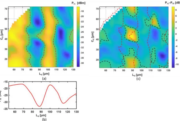
To better highlight this behavior and to deduce design rules useful for the correct positioning of crossing waveguides in the network, parametric maps have been obtained by calculating the received power PRCas a function of Cdand Ld.
Fig. 5(a) shows the received power PRCcalculated in the presence of the crossing waveguide, as a function of the Ld and Cd parameters. For the sake of direct comparison, we also report in Fig. 5(b) the simulated received power Pr0 in EWC as a function of Ld. In Fig. 5(a) and (b), the maximum excursion of the received power is about 15–20 dB, caused by constructive and destructive interference of the rays composing the overall signal propagating in the on-chip multilayer structure. In particular, we can see in Fig. 5(a) that, given a fixed value of the crossing distance Cd, it is possible to distinguish Ldvalues for which the signal assumes high values (yellow regions contoured by red dotted lines), and others for which it is significantly lower (green-blue
IEEE Photonics Journal
Numerical And Experimental Analysis
Fig. 5. (a) Received power PRCin the SOWC case, expressed in dBm, as a function of the crossing
distance Cd and the link distance Ld; The red dashed contour lines identify the reference received
power level Pr= −25 dBm. (b) Received power Pr0in the EWC case, expressed in dBm, as a function
of the link distance Ld. (c) Map representing the difference PRC−Pr0in dBm between the received
powers in the EWC and in the SOWC cases. Red dashed contour lines identify the reference received power level Pr = −25 dBm, whereas the black dashed contour lines identify the values for which
(PRC−Pr0)= 0 dB.
zones). The PRC reference value chosen to identify the transition from the high to the low signal regions is −25 dBm (red dotted curves). The choice of the reference value is in agreement with [23], and it guarantees a bit-error-probability (BEP) lower than 10−6for a standard receiver.
Moreover, by comparing Fig. 5(a) and (b), we can see that, for different Cd values, the high and low signal regions qualitatively follow the trend of the received power Pr0 in the EWC case. However, perturbations of the received power are indeed induced by the crossing waveguide. To better quantify this perturbation, we report in Fig. 5(c) the difference (in dB) between the received power PRCin the SOWC case and the received power Pr0in the EWC case, as a function of the crossing distance Cdand of the link distance Ld. The reference value (−25 dBm) chosen to identify the transition between the high and low signal regions is also shown in Fig. 5(c) (red dotted curves). Moreover, Fig. 5(c) shows the contour curves corresponding to 0 dB difference between PRCand Pr0(black dashed curves).
The comparison of Fig. 5(b) and 5(c) shows that the insertion of the crossing waveguide in links with Ldcorresponding to high Pr0levels is likely to be harmful almost regardless of the Cdvalue. For example, the insertion of a crossing waveguide causes a reduction of the received power (i.e., Prc−Pr0< 0 dB) for Ld values around Ld = 70 μm or Ld = 100 μm, independently from the Cd values. Conversely, when the waveguide is inserted in a link experiencing a weak received power Pr0, it can result in some kind of benefit (as an example the increase occurs around Ld= 90 um for Cd= 12 μm and Cd= 48 μm). Overall, this is not fully surprising. In fact, as long as on-chip optical propagation is dominated by multipath effects [24], the introduction of potential scatterers between the antennas can completely change the ray pattern and even reverse the final interference effect.
Therefore, the crossing waveguide is more likely to act as an impairment when the interference at the receiver in the EWC case is constructive, whereas it may more easily represent a benefit when a destructive interfering effect is already suffered before its introduction. There are also small pockets where the constructive effect is present in high power regions.
By following this approach, given a multilayered on-chip structure, multi-parametric maps, such as those shown Fig. 5, can be created for the correct placement of crossing waveguides in the wireless link. After the definition of the maps, it is possible to select the most suitable combination of Cd and Ld parameters according to the network design constraints. As an example, to ensure better link performance, the best positions for the receiver correspond, in Fig. 5(a), to received powers higher than−25 dBm, whereas the position of the crossing waveguide can be chosen from the design maps to minimize the perturbation of the received signal (e.g., around the black dashed lines corresponding to Prc−Pr0= 0 dB).
In addition to the analysis of the received power, we evaluated the crosstalk between the wireless link and the crossing waveguide. For this purpose, the received power PWG values at the two ports of the crossing waveguide were evaluated when the signal was launched in input to the transmitting antenna. We have verified that the levels of PWG are below −65 dBm in the FDTD analysis, whereas they are in the range from−50 dBm to −40 dBm in the experimental results. The low value of the coupling, which is beneficial for the network as it demonstrates low crosstalk between the links, can be attributed to the lack of structures promoting coupling between unbound signal and waveguide mode (i.e., antennas and taper tips), and also to the perpendicular position of the waveguide with respect to the wireless link.
6. Conclusion
In this paper, we have shown, through an extensive use of simulations and experiments, that the presence of obstacles in an on-chip wireless channel perturbs the electromagnetic field of the wireless signal, altering the multipath propagation and consequently the received power. The simulations have shown the possibility of locating the positions with high and low received power levels related to constructive and destructive interferences.
The results of the characterization of a fabricated sample, housing different wireless link with obstacles, have been reported. The simulations and the measurements are in very good agreement (i.e., difference smaller than 1 dB) when considering higher levels of the received power. Thanks to the good agreement between numerical and experimental results, we have demonstrated that the effects of the perturbation induced by obstacles in real chips can be efficiently predicted by numerical modelling. In particular, these scatterers generally reduce the amount of the overall received power, but it is possible to mitigate losses or even to obtain an improvement of the received power by suitably designing the link topology through correct placement of receivers and perturbators. To this aim, design maps have been obtained by numerical simulation that allow the identification of the positions featuring constructive and destructive interference.
We demonstrated that an accurate positioning of both the crossing waveguide and the receiver allows to minimize the effect of the perturbation and eventually to reduce losses, or even to improve the level of the received power. Therefore, the use of suitable maps, obtained by the proposed parametric analysis, allows for optimized topological choices.
Moreover, we verified that the crosstalk signal on the crossing waveguide is very small, due to the lack of structures promoting coupling between unbound signal and waveguide mode (i.e., antennas and taper tips), and also due to the perpendicular position of the crossing waveguide with respect to the wireless link.
The analysis reported in this paper is also useful for the comprehension and interpretation of what happens in more structured systems that include multiple objects and it represents a necessary step towards the actual implementation of on chip wireless communications. Moreover, the results of this study can be used also for a better understanding of unbound optical signals within the chip environment, as well as enhance emerging applications such as beam steering, beam forming, biosensing on-chips.
IEEE Photonics Journal
Numerical And Experimental Analysis
Acknowledgment
Gaetano Bellanca, Jinous Shafiei Dehkordi and Velio Tralli acknowledge “Bando per l’acquisizione di strumenti per la ricerca di Ateneo - Anno 2015” of the University of Ferrara. The authors thank INPHOTEC Foundation for the fabrication of the devices.
References
[1] D. A. Miller, “Rationale and challenges for optical interconnects to electronic chips,” in Proc. IEEE, 2000, vol. 88, pp. 728–749.
[2] R. Kumar, D. M. Tullsen, N. P. Jouppi, and P. Ranganathan, “Heterogeneous chip multiprocessors,” Computer, vol. 38, no. 11, pp. 32–38, Nov. 2005.
[3] A. H. Atabaki et al., “Integrating photonics with silicon nanoelectronics for the next generation of systems on a chip,”
Nature, vol. 556, pp. 349–353, 2018.
[4] A. Biberman, B. G. Lee, N. Sherwood-Droz, M. Lipson, and K. Bergman, “Broadband operation of nanophotonic router for silicon photonic Networks-on-Chip,” IEEE Photon. Technol. Lett., vol. 22, no. 12, pp. 926–928, Jun. 2010. [5] S. Werner, J. Navaridas, and M. Lujan, “A survey on optical Network-on-Chip architectures,” ACM Comput. Surv.,
vol. 50, no. 89, p. 37, 2017.
[6] B. Alam, A. Veroli, and A. Benedetti, “Analysis on vertical directional couplers with long range surface plasmons for multilayer optical routing,” J. Appl. Phys., vol. 120, 2016, Art. no. 083106.
[7] S. Majumder and R. Chakraborty, “Multilayered photonic integration on SOI platform using waveguide-based bridge structure,” Eur. Phys. J. Appl. Phys., vol. 81, no. 3, 2018, Art. no. 30501.
[8] D. Matolak, A. Kodi, S. Kaya, D. DiTomaso, S. Laha, and W. Rayess, “Wireless networks-on-chips: Architecture, wireless channel, and devices,” IEEE Wireless Commun., vol. 19, no. 5, pp. 58–65, Oct. 2012.
[9] S. Deb, A. Ganguly, P. P. Pande, B. Belzer, and D. Heo, “Wireless NoC as interconnection backbone for multicore chips: Promises and challenges,” IEEE J. Emerg. Sel. Topics Circuits Syst., vol. 2, no. 2, pp. 228–239, Jun. 2012. [10] C. García-Meca et al., “On-chip wireless silicon photonics: From reconfigurable interconnects to lab-on-chip devices,”
Light Sci. Appl., vol. 6, 2017, Art. no. e17053.
[11] Y. Yang, Q. Li, and M. Qiu, “Broadband nanophotonic wireless links and networks using on-chip integrated plasmonic antennas,” Sci. Reps, vol. 6, 2016, Art. no. 19490.
[12] G. Bellanca, G. Calò, A. E. Kaplan, P. Bassi, and V. Petruzzelli, “Integrated vivaldi plasmonic antenna for wireless on-chip optical communications,” Opt. Exp., vol. 25, no. 14, pp. 16214–16227, 2017.
[13] M. Elsaid, K. R. Mahmoud, M. F. O. Hameed, S. S. A. Obayya, and M. Hussein, “Broadband directional rhombic nanoantenna for optical wireless communications systems,” J. Opt. Soc. Am. B, vol. 37, pp. 1183–1189, 2020. [14] X. D. Fan and I. M. White, “Optofluidic microsystems for chemical and biological analysis,” Nat Photon., vol. 5,
pp. 591–597, 2011.
[15] L. Zhuang et al., “Novel ring resonator-based integrated photonic beamformer for broadband phased array receive antennas—Part II: Experimental prototype,” J. Lightw. Technol., vol. 28, no. 1, pp. 19–31, Jan. 2010.
[16] N. Yu and F. Capasso, “F. Flat optics with designer metasurfaces,” Nat. Mater., vol. 13, pp. 139–150, 2014. [Online]. Available: https://doi.org/10.1038/nmat3839
[17] M. Uysal, C. Capsoni, Z. Ghassemlooy, A. Boucouvalas, and E. Udvary, Optical Wireless Communications. Berlin, Germany: Springer International Publishing, ISBN 978-3-319-30201-0, 2016.
[18] G. Calò, G. Bellanca, A. E. Kaplan, P. Bassi, and V. Petruzzelli, “Double vivaldi antenna for wireless optical networks on chip,” Opt. Quant. Electron., vol. 50, p. 261, 2018. [Online]. Available: https://doi.org/10.1007/s11082-018-1511-3 [19] G. Calò, G. Bellanca, B. Alam, A. E. Kaplan, P. Bassi, and V. Petruzzelli, “Array of plasmonic vivaldi antennas
coupled to silicon waveguides for wireless networks through on-chip optical technology-WiNOT,” Opt. Exp., vol. 26, pp. 30267–30277, 2018.
[20] G. Calò et al., “Dielectric and plasmonic vivaldi antennas for on-chip wireless communication,” in Proc. 21st Int. Conf.
Transparent Opt. Netw., Angers, France, 2019, pp. 1–4.
[21] M. Nafari, L. Feng, and J. M. Jornet, “On-Chip wireless optical channel modeling for massive multi-core computing architectures,” in Proc. IEEE Wireless Commun. Netw. Conf., San Francisco, CA, 2017, pp. 1–6.
[22] F. Fuschini, et al. “Ray tracing modeling of electromagnetic propagation for on-chip wireless optical communications,”
J. Low Power Electron. Appl., vol. 8, no. 4, p. 39, 2018.
[23] F. Fuschini et al., “Multi-Level analysis of on-chip optical wireless links,” Appl. Sci., vol. 10, no. 1, 2020, Art. no. 196. [24] J. Nanni et al., “Multi-Path propagation in On-chip optical wireless links,” Photon. Technol. Lett., vol. 32, no. 17,
pp. 1101–1104, 2020.