1
Alma Mater Studiorum - Università di Bologna
SCUOLA DI SCIENZE
Dipartimento di Chimica Industriale “Toso Montanari”
Corso di Laurea Magistrale in
Chimica Industriale
Classe LM-71 - Scienze e Tecnologie della Chimica Industriale
Physisorption of perylene dyes on graphite
Tesi di laurea sperimentale
CANDIDATO
Luca Ferraro
RELATORE
Chiar.mo Prof. Maria Cristina Cassani
CORRELATORE
Dr. Vincenzo Palermo Dr. Andrea Liscio Dr.ssa Vanesa Maria Quintano
________________________________________________________________________________________________________________________ Anno Accademico 2017-2018
3
ABSTRACT
This thesis work was carried out at CNR (Council of National Research) of Bologna. CNR- ISOF (Institute of Organic Synthesis and Photoreactivity) in the group of Dr. Vincenzo Palermo.
The aim of this thesis was to perform a comparative and quantitative study on the interaction of three different PDI (perylene diimide) dyes with graphene (G) sheets in solution, using a phenomena called “dye‟s capturing”.
The only difference between the PDI dyes tested was the terminal atom in the side groups. In particular, we used a perylene core with side ethyl-phenyl group exposing in the para position a hydrogen (PDI-H), fluorine (PDI-F), or chlorine atom (PDI-Cl).
Although the relative simplicity of the process and the measurement itself, the preparation of a reliable experimental setup is not trivial and several issues had to be taken into account.
The main challenges to be overcame were related to the effective stability and reliability of the chemical systems, such as dyes, solution and graphite during the entire exposure time.
For this reasons the work addressed the following issues:
Studying the interaction of small organic molecules and graphite flakes, using commercial products.
Finding the best conditions for the dye capturing process (concentration, stabilization of the solution, solvent etc.).
Understanding of the “dye‟s capturing” phenomena by UV-VIS and fluorescence techniques.
Stabilizing a relationship between the chemical structure of PDI-X (with side chains symmetrically terminated with a different atom) and the interaction with graphite, taking into account adsorption speed, packing, etc.
After testing the samples, the reported results were used to: Determinate the best suitable molecule for the dye capturing process and optimize a hypothetical industrial process by calculating the surface area for each molecule.
Morphology and structural characterizations with different technique like: Atomic force microscopy (AFM), Scanning electron microscopy (SEM), Energy-dispersive X-ray spectroscopy (EDS/EDX), X-ray diffraction (XRD), fluorescence microscopy, Thermogravimetric analysis and differential scanning calorimetry (TGA/DSC), Infrared (IR)
4
INDEX:
1)Introduction ... 7
1.0 Carbon Materials retrospective ... 7
1.1 Graphite ... 8
1.2 Diamond ... 9
1.3 Diamond-like carbon (DLC) and amorphous carbon ... 9
1.4 Fullerenes and nanotubes ... 10
1.5 Graphene and 2D materials ... 11
1.5.1 Classification of 2D materials based on dimension ... 13
1.5.2 Zero dimensional (0D) ... 13 1.5.3 One dimensional (1D) ... 14 1.5.4 Three dimensional (3D) ... 15 1.5.5 Two dimensional (2D) ... 15 1.6 Synthesis of graphene ... 16 1.6.1 Exfoliation ... 16 1.6.2 Mechanical exfoliation ... 17 1.6.3 Chemical exfoliation ... 18 1.6.4 Epitaxial grow ... 20
1.6.5 Chemical vapor deposition (CVD) ... 21
1.6.6 Liquid phase exfoliation ... 24
1.5.5 Liquid phase extraction with organic dye ... 26
1.7 Graphene proprieties ... 27
1.8 Potential applications ... 30
1.9 Chemically derived of graphene ... 33
1.9.1 Graphene oxide ... 33
1.9.2 Reduced graphene oxide ... 35
1.9.3 Electrochemical exfoliation ... 36
1.9.4 Total organic synthesis ... 38
1.10 Perylene dimmide family ... 39
1.10.1 The use of PDI’s as pigment in industry ... 39
1.10.2 Physical proprieties of PDI’s ... 42
5
1.10.4 Molecular packing of PDI’s in the solid state ... 44
1.10.5 Redox proprieties of PDI’s ... 45
1.10.6 Application of PDI dyes in organic electronic (OFETs andOPVs) ... 46
1.10 Reference chapter I ... 50
2)Theoretical principle ... 56
2.1 Spectrophotometer technique ... 56
2.2 Spectroscopy based on emission ... 59
2.3 Surface are and pore structure by gas adsorption (BET) ... 60
2.4 TGA ... 62 2.5 DSC ... 63 2.6 ICP ... 65 2.7 XRD ... 67 2.8 EDX/EDS ... 68 2.9 SEM ... 69
2.10 Particle size distribution ... 71
2.11 AFM ... 72
2.12 Fluorescence microscopy ... 74
Reference chapter II ... 76
3) Analytical methods for the determination of the interaction between perylene diimides and graphite substrate ... 77
3.1 Spectrophotometric assay ... 77
3.2 Fluorescence assay ... 79
3.3 BET surface area measure ... 80
3.4 Granulometer measure ... 82
3.5 TGA/DSC and ICP analysis ... 84
3.6 SEM&EDX measure ... 86
3.7 AFM measure ... 87
3.8 Fluorescence microscopy measure ... 88
3.9 XRD measure ... 90
4)Results ... 92
4.1 Spectrophotometer analysis ... 93
4.2 Fluorescence analysis ... 113
6
4.4 Granulometer measure ... 123
4.5 TGA/DSC, ICP and IR analysis ... 127
4.6 SEM&EDX analysis ... 138
4.7 AFM analysis ... 143
4.8 Fluorescence microscopy analysis ... 147
4.9 XRD analysis ... 154
Reference chapter IV ... 162
8
Chapter I - INTRODUCTION
1.0 Carbon materials retrospective
Carbon is one of the most important elements in our life, and it is the fourth most abundant chemical element in nature. Not only constitutes one of the basic elements for life (an average representation of carbon in the mass of living matter is 19.4%); it is also widely used in industry for materials manufacturing. The fundamental feature of carbon is its unique capability for combining with other elements. For example, the so-called hydrocarbons are formed by the grouping of carbon and hydrogen atoms either in chains or in rings. The addition of methyl radicals, nitrogen, oxygen and other new elements provides more complex molecules (acids, alcohols, etc.), whose periodical attachment leads to polymeric structures.
In order to understand why carbon achieves such an elevated coordination degree, we must study its electronic structure. Carbon occupies the 6th position within the periodic table, which provides an electron configuration at ground state of 1s2 2s2 2p2. figure 1 shows a scheme of the electron distribution in atomic orbitals, where the arrows indicate the spin polarization.[1]
Figure 1: Electron distribution in the carbon orbitals for a carbon atom with valence number 2. The subindex x, y and z indicate the orientation of p orbitals with respect to the corresponding axis. This differentiation is not
required in s orbitals, since they are spherical.
Electronic orbitals of the carbon atom contain only two unpaired electrons, behaving thus as bivalent element. In order to justify the tetravalence of carbon, one of the two electrons from the 2s orbital must occupy an empty 2p orbital. As a result of the previous redistribution, carbon has four dangling bonds and all the electrons in the outer layer are unpaired. Then, the linear combination of s and p atomic orbitals generates the so-called hybrid orbitals. Hybridization comprises three cases: The s orbital together with one p gives rise to two sp orbitals, when two p orbitals are added to s we obtain three sp2, and finally, the hybridization of all the orbitals from the second layer provides four sp3. Figure 2 shows the possible geometric configuration in the carbon atom depending of the type of hybridization. Diametrically opposed orientation takes place in the case of sp orbitals. In this configuration, both sp orbitals make strong frontal σ bonds to an adjacent atom, whereas there are two weak lateral π bonds with neighboring p orbitals.
9 On the other hand, trigonal planar configuration is typical of sp2, which form σ bonds. The pure p orbital forms a π bond. Finally, sp3 lobes are oriented towards the vertexes of a regular tetrahedron. In this case, all the four orbitals are hybridized and form σ bonds.
Figure 2: Spatial arrangement of orbitals in the carbon atom in the case of (a) sp, (b) sp2 and (c) sp3
hybridizations. 1
Carbon presents allotropy, i.e. three main different phases have been found in solid state: graphite, diamond, and amorphous carbon. They are constituted by carbon atoms bonded by sp2, sp3 and combinations of both hybridizations, respectively. There exists another configuration of carbon: the polymer-like form. It is found when carbon is diluted with hydrogen, and it presents low hardness, high transparency, and electrically it behaves as an insulator. The spatial distribution of polymeric carbon comprises a rich variety of shapes and lengths, which gives rise to compounds with different chain types. They are divided into aliphatic (lineal, branched, or alicyclic) and aromatic (benzene, etc.) Below, we find summarized some of the most important carbon allotropes.
1.1 Graphite
Graphite shows a stable trigonally bonded crystal structure (figure 3). Carbon atoms become bonded by σ bonds due to three superposed sp2
orbitals, adding a π bond that results from the interaction of pure p orbitals. This material is soft, optically opaque, chemically active, and is a good electric conductor. The atoms are organized in parallel and single-atom planes, which are called graphene layers and are the center of this thesis. Carbon atoms from adjacent planes are bonded by weak dispersion van der Waals forces, which allow two layers of graphene to slip one on
10 each other and confers softness and special lubricating properties to graphite. The in-plane bond length is 0.142 nm, whereas the inter-plane distance is 0.335 nm. Graphite crystallizes in hexagonal closepacked (h.c.p.) network, and its most important applications are pencil tips, electrodes, and solid lubricants.[1]
1.2 Diamond
Diamond structure results from the metastable tetragonal σ bonding of carbon atoms, and is only stable at high pressure and high temperature. It is considered to be a material with various extreme physical properties. First of all, it exhibits the highest elasticity module known to date. In fact, diamond establishes the ultimate hardness limit basically due to the superior strength of its chemical bonds. Complete sp3 hybridization occurs and, therefore, all atoms become bonded via strong frontal σ bonds. The C-C bond (sp3) is 0.154 nm long, a bit longer and weaker than that in graphite (sp2), and its crystallographic structure consists of two superimposed face-centered cubic (f.c.c.) lattices shifted by one-quarter of the cube diagonal (figure 1.3). Such bonds confer the extreme hardness of diamond, and the highest atom density among all solids. Diamond is mostly employed in cutting tools (edges), abrasive coatings (dust), and jewelry. A prominent use of diamond in electronic applications has taken place due to the interesting properties when the material is chemically doped, especially in superconductivity applications.[2] Diamond conventional preparation requires high-pressure and high temperature processes (HPHT). Thin films of single crystal diamonds in thin film form are usually prepared by CVD method at high deposition rates. Furthermore, there is also a hexagonal diamond called Lonsdaleite (named in honor of Kathleen Lonsdale). In nature, it forms when meteorites containing graphite strike the Earth. The great heat and stress of the impact transforms the graphite into diamond, but retains graphite's hexagonal crystal lattice. It is theoretically harder (58% more) than conventional diamond but it is not demonstrated in practice, where impurities and lattice defects play a fundamental role.[3]
1.3 Diamond-like carbon (DLC) and amorphous carbon
Besides diamond and graphite, carbon can form an amorphous phase. Amorphous carbon (a-C) is obtained under controlled deposition of the amount of diamond, graphite, and polymeric phases.[4] Its close relationship with DLC is currently defined by the IUPAC as:
Diamond-like carbon (DLC) films are hard, amorphous films with a significant fraction of sp3-hybridized carbon atoms and which can contain a significant amount of hydrogen.
11 Depending on the deposition conditions, these hard films can be fully amorphous or contain diamond crystallites.[5]
Amorphous carbon is a carbon material without long-range crystalline order. Short range order exists, but with deviations of the interatomic distances and/or interbonding angles with respect to the graphite lattice as well as to the diamond lattice.[6]
The DLC matrix does not contain only one determined hybridization, but contains all three in different proportions. Preparation of a-C containing large sp3/sp2 ratio is desirable to obtain “diamond-like” properties. In this way, plasma deposition techniques like sputtering and Plasma Enhanced Chemical Vapor Deposition (PECVD) increase sp3 bonding, although the latter technique provides H-rich samples. High plasma density PECVD reactors are necessary to maximize sp3 bonding and simultaneously diminish hydrogen content. When the sp3 fraction reaches a high degree (80-88%), a-C is denoted as tetrahedral a-C (ta-C) because tetrahedral bonding due to this hybridization is predominant.[7] We can imagine the microstructure as a system of covalently bonded carbon atoms organized in a 3D network, containing a random distribution of sp2 and sp3 bonds (figure 1.3). Polymeric carbon can also host a great fraction of sp3 bonds, although the majority of them come from C-H groups and therefore the material is soft. This ensures a rich variety of a-C microstructures and properties.
1.4 Fullerenes and nanotubes
Although there already were a very well-known variety of carbon based materials (graphite, diamond, and a-C), a more exotic forms of carbon were about to appear. Buckminster fullerenes were introduced in 1980s as an additional form of carbon. They were formulated as C60, and
consisted on spherical lattices formed by 60 sp2-bonded carbons (figure 1.3). Extensive research on fullerenes has been undertaken for medical applications using fullerenes as substitutive ligands or in biosensor devices. In the early 1990s, even a subset of fullerene science appeared. C70, C76, C82, and
C84 are other common members of the fullerene family. They are present in soot and produced in
nature by lightning discharges in the atmosphere. Even a giant icosahedral molecule C540 can be
seen within interstellar gas clouds. However, the expectations of these “carbon balls” quickly decreased.8 Right after, in 1991, Ijima reported the preparation of new cylindrical structures called carbon nanotubes. They were called multiwalled nanotubes (MWCNT), since they consisted on multiple graphene layers that formed a cylinder surface (figure 1.3).[9] Further refinements permitted the deposition of single-wall nanotubes (SWCNT), whose chirality determines their electric properties. Both fullerenes and nanotubes were initially grown by arc discharge and laser
12 ablation techniques, and recently they have been produced by CVD method. Most carbon nanotubes applications include field emission devices, fuel cells, cold cathodes, and ultrahigh-strength structural materials. Few people in the world had any idea that another, and probably the definitive “son” of the carbon was about to get into the stage:
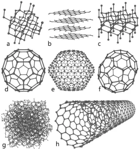
Figure 3:The structures of eight allotropes of carbon: (a) Diamond, (b) Graphite, (c) Lonsdaleite, (d) C60
(Buckminsterfullerene), (e) C540 Fullerene, (f) C70 Fullerene, (g) Amorphous carbon, and (h) Single-walled
carbon nanotube.[10]
1.5 Graphene and 2D materials
The discovery and research of carbon materials has considerably contributed to the advancement of modern day science and technology. After the discovery of fullerene and single walled carbon nanotube (CNT), which are zero-dimensional and one-dimensional carbon nanomaterials respectively, the researchers have tried to isolate 2D graphitic material or to make 1D nano-ribbons from 2D crystals.
Progress in graphene research had a spillover effect by way of leading to an interest in other 2D materials like for example metal nitrides and carbides. 2D nanostructures are one of the greatest
13 widely studied materials because of the unique physical singularities that happen when heat transport and charge is confirmed to a plane. Due to the unique properties, 2D nanostructures are anticipated to have an important influence on a huge diversity of applications, extending from high performance sensors, electronics to gas separation or storage, catalysis, inert coatings and support membranes, etc. Right now, the 2D materials family includes not just carbon material but also transition metal dichalcogenides (TMDs), and layered metal oxides. One of the most promising applications of 2D materials is in electronic devices. [11] With respect to the electrical properties, one can fabricate a new generation of superconductors, metallic materials, semimetals, semiconductors, insulators from the 2D materials. Despite the similarity in the chemical formula, MX2, where typically M is transition metal of groups 4–10 (typically Mo, Nb, W, Ni, V, or
Re),[12,13] and X is a chalcogen (typically Se, Te, or S)[14,15]. While the bonding of the tri-layers are covalent, neighboring sheets are bonded via Van der Waals interactions to grow 3D crystals. There are currently 40 different types of combination of TMDs with different chalcogen atoms. Based on the co-ordination and oxidation state of the metal atoms, TMDs ranging from insulators such as HfS2, semiconductors such as MoS2, semimetal such as TiSe2, to true metals such asNbSe2,
which can even exhibit superconductivity at low temperature.[16,17] Table 1 lists all the current members in the 2D layered materials family.[18] However, stability is a critical issue. The blue shaded materials are constant under ambient environments (room temperature in air) for monolayers. Perhaps green shaded materials are stable in air, but those may be steady only in inert atmosphere are shaded pink. Gray shading means monolayer has been exfoliated, but no further information has yet been provided other than atomic force microscope (AFM). Furthermore, this layered 2D materials exhibits a combination of excellent electronic,[19] mechanical,[20] optical,[21] and thermal properties,[22] which may substitute silicon in electronics, photonics, and nano electromechanical system.
14
Table 1:2D materials family[16]
There are many layered materials with strong in-plane chemical bonds and weak coupling between layers. These layered structures provide the opportunity to be cleaved into individual freestanding atomic layers. When the thickness of layered material is reduced to single or only few layers, some extraordinary variations occur in their electronic properties. Due to their symmetry, and high porosity, nanofilms coated with thin layers of inorganic graphene like materials have potential applications from ultralight anti-corrosive materials to electron field emitters. [23,24]
1.5.1: Classification of materials based on dimension
Nanostructured materials (NSMs) are defined as solid materials characterized by at least one dimension in the nanometer range. A crystalline material having at least one dimension smaller than 100 nm is said to be a nanomaterials.
1.5.2 Zero dimensional (0D)
The density of states of quantum-confined nanocrystals has characteristic shapes for different dimension nanomaterials and the differences are due to the degree of confinement of the electrons. For 0D NSMs, the excited electrons are completely confined in all the three dimensions and they behave analogous to atomic/molecular clusters with discreet states that are well separated in energy. Different types of 0D NSMs images are shown in figure 4. Furthermore, 0D quantum dots has been widely considered in solar cells,[25] light emitting diodes (LEDs),[26] lasers,[27] and single-electron transistors.[28]
15
Figure 4: Electron microscope image of various 0D NSMs synthesized by several research groups. (a) Quantum dots,[25] (b) nanoparticles binary arrays, [26] (c) hollow core –shell nanoparticles, [27] (d) hollow sphere, [28]
and (e) hollow MoS2 nanospheres.[29] Reprinted by permission of ACS Publishers
1.5.3 One dimensional (1D)
1D nanomaterial has nano-scale sizes along two dimensions and having a rod or wire-like appearance. In such nanomaterials, quantum confinement and surface area related nanoscale effects are more pronounced compared to 2D nanomaterials, while at the same time they can be integrated and/or connected into device architectures due to single bulk-like dimension that is absent in 0D nanomaterials. In the previous decade, interest in 1D materials have increased because of their importance in an extensive range of potential applications such as optoelectronic, and electronic in nanoscale dimensions. Due the differences in quantum mechanical parameter of electron and phonon transport[29],it has been theoretically shown that nanowires of certain alloys can be made to have good electronic conduction with decreased thermal conduction, [30] showing good potential for high performance thermoelectric materials.[31] In figure 5 has been shown some images of various 1D NSMs.
16
Figure 5: Electron microscope image of various 1D NSMs. (a) Nanowires[29], (b) nanorods[30], (c) nanotubes[31], (d) nanobelts[32], (e) nanoribbons[33], and (f) hierarchrial nanostructures[34]. Reprinted by
permission of ACS Publisher
1.5.4 Three dimensional (3D)
3D nanostructures have concerned significant attention in the recent years due to high surface area and physicochemical properties when compared to their bulk materials due to quantum size effects.[30,33] It is long-familiar that the performances of these materials, mainly depend on the shape, size, morphologies, and dimensionality, which are considered to be an important role in their quality execution and applications. Additionally, these well-ordered and innovative 3D NSMs are used in many different applications such as electrode materials for batteries, catalysis, and magnetic material.[31] Then again, 3D NSMs are highly porous materials with 3D could extend to a superior conveyance of the molecules for the catalytic application.
1.5.5 Two dimension (2D)
There are many layered materials with strong in-plane chemical bonds and weak coupling between the layers. These layered structures provide the opportunity to be cleaved into individual freestanding atomic layers. These layers with one dimension strictly restricted to a single layer are called two-dimensional (2D) material. 2D inorganic materials have received great interest recently, because of their particular physical properties due to the quantum size effect, which is related to their nanosized thickness. In addition, at a particular point both the valence band and conduction band touch each other in 2D materials,[35] offering only certain electronic state near the Fermi level thus these materials called zero gap semiconductor or semimetal. The band structure of 2D NSMs is highly sensitive to any change because of their brittleness in single point contact such as mechanical
17 deformations, external electric fields, doping and adsorbents; which is necessary for sensor applications. This is similarly discussed an ambipolar part onto 2D NSMs, i.e. charge carrier contains either electrons or holes depending on dopant material.[36] However, doping is not continually necessary to alter the charge carrier, local electric fields can also modify the charge carrier sign. This peculiar property of 2D material plays an important role in creating p–n junction transistors with high mobility and this is the base of existing complementary metal oxide semiconductor (CMOS) technology. The 2D material‟s electronic band structures are equally interesting.
The zero band gap of these materials allows the large range of light absorption in the possible electromagnetic spectrum, extending from the infrared (IR) to the ultraviolet (UV).[37] This opens up a huge number of options of electronic transition resulting in high performance optoelectronic devices and other basic essential studies related to optics and photonics.[38] Simultaneously, a few layers of 2D material present absorbance of less than 10% and in single layered material, it is 2.3%, which may be due to their thickness and transparency.[39] This extraordinary opaque property joined together with their excellent conductivity makes them highly applicable as transparent electrodes in many electronic devices, including solar cell and liquid crystal devices. 2D materials are extremely very strong as graphene ever tested. It gives an extraordinary breaking strength, compare to steel it is 200 times higher and also these materials are unpredictably flexible.
This makes the 2D material a desirable addition to lightweight polymer, and the enforcer of their mechanical properties.
1.6 Synthesis of graphene
1.6.1 Exfoliation
Recently, much attention has turned to the structural and electronic properties of carbonbased materials. At present, especially, graphene is the hottest topics in condensed-matter physics and materials science. This is because graphene has not only unusual properties regarding extreme mechanical strength, thermal conductivity and 2-diemensional films, but also peculiar electronic characteristics such as Dirac-particles with a linear dispersion, transport energy gap and simply absorption coefficient of lights. It is obvious that these excellent properties are relevant at the nanoscale and the manufacture of the conducting nanocomposites is highly dependent on the exfoliation of the graphite down to single graphene sheet in the matrices. However, the challenge remained to achieve complete and homogeneous dispersion of individual graphene sheets in various
18 solvents.[40] Like CNT and other nanomaterials, the key challenge in synthesis and processing of bulk-quantity graphene sheets is aggregation. Graphene, a one-atom-thick planar sheet of sp2 -bonded carbon atoms densely packed in a honeycomb crystal lattice has very large specific surface area. Unless well separated from each other, graphene tends to form irreversible agglomerates or even restack to form graphite through Van der Waals interactions. The prevention of aggregation is essential for graphene sheets because most of their unique properties are only associated with individual sheets.[40]
There are different synthesis methods lead to “different qualities and characteristics” of the graphene produced. Ones may be close to “perfect”, mainly for research purposes but extremely expensive. Others may not be that “perfect” but cheap enough to make it real and carry it to the industry. Among them, Chemical Vapor Deposition (CVD) process (e.g. on copper, nickel, ruthenium…) seems to meet both requirements in quality and cost, as shown in figure 6.
Figure 6: Plot of the main graphene synthesis methods regarding quality and cost (Y-axis) and scalability (X-axis)
1.6.2 Mechanical exfoliation
Also mentioned as micromechanical cleavage, mechanical exfoliation was the first technique used to isolate one monolayer of graphite in 2004. It is possible due to the weak bonds between the atomic planes of graphite. The Van Der Waals interactions between planes are of the order of 2 eV/nm2. Then, the required normal force to cleave off a 1 µm2 graphite sheet from the top of the crystallite is about 300 nN, considering 1 µm as path and assuming as unity the graphene-substrate friction coefficient (adhesion is an important friction mechanism at low normal loads).[1] The force
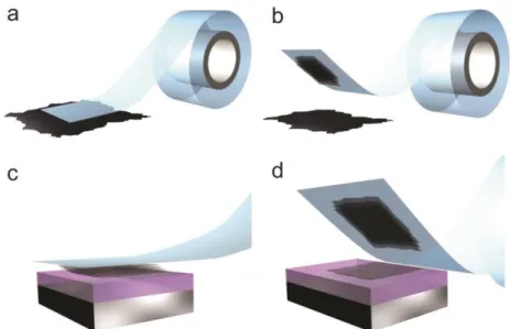
19 can be exerted using an adapted AFM tip or, more simply, by the resistance to the release of a conventional scotch tape. The last method was the one used to obtain the first isolated graphene sheets based on repeating peeling of highly oriented pyrolytic graphite (HOPG),[1] as seen in figure 7. This process statistically results in some graphene monolayer flakes (among bi, tri and few-layer graphene) which can be transferred to different substrates, usually silicon/silicon dioxide for subsequent characterization purposes.
Figure 7: Step by step of a mechanical exfoliation process: (a) adhesive tape is pressed against a HOPG surface so that the top few layers are attached to the tape (b),(c)the tape with crystals of layered material is pressed
against a surface of choice , and (d) upon peeling off, the bottom layers is left on the substrate
Nowdays, graphene obtained by mechanical exfoliation is the one which presents the best electronic properties and less crystalline defects, but the difficulties for scaling up the process and to make it compatible with the existent technologies have triggered the investigations to other fabrication techniques. Another drawback of this method is the size of the flakes. In the best of cases, one can obtain flakes of 20x20 µm2, which can be enough for several fields of research but not suitable for industrial purposes. This method is also useful to obtain monolayers of MoS2 and h-BN(hexagonal
boron nitride).[1]
1.6.3 Chemical exfoliation:
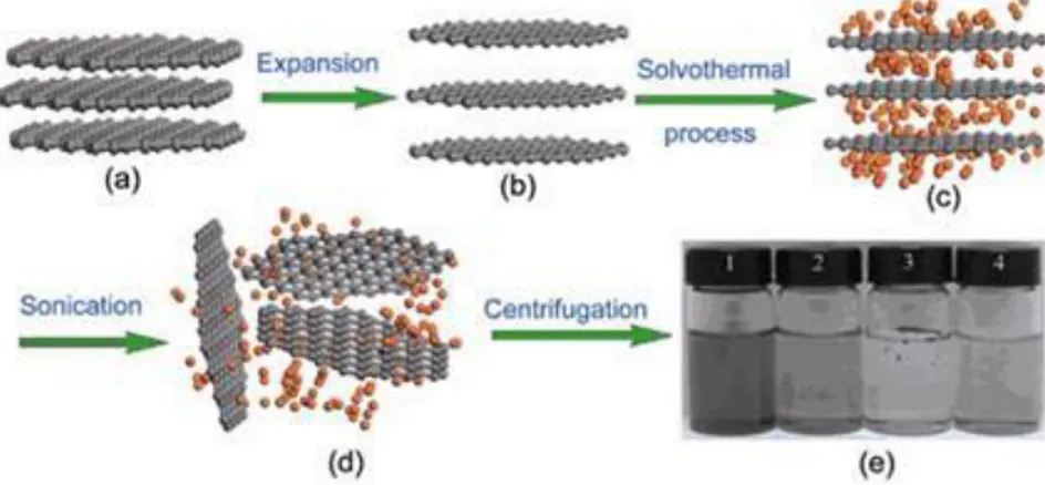
Another possibility is to obtain graphene via wet chemical routes like chemical exfoliation, which consists in the intercalation of a reactant among the graphene sheets (of graphite) that softens the van der Waals interactions. This is achieved immersing graphite in an acid solution (sulfuric and/or nitric acid). The soften interlayer interactions will be broken then, by means of two steps: first, a thermal process (solvothermal), and finally ultra-sonication to disperse them. The result consists in
20 graphene oxide sheets suspended in a colloidal solution, which are deposited on a substrate (figure 8). For the final objective of obtaining pure graphene flakes, the oxide has to be removed in a reducing atmosphere using alkaline solutions, or applying hydrogen plasma, or hydrazine vapours, figure 8, or through heat treatments. Graphene flakes partially oxidized are obtained because, unfortunately, the reduction processes are not very efficient.[41]
Figure 8: Solvothermal-assisted exfoliation and dispersion of graphene sheets: (a) pristine expandable graphite, (b) expanded graphite, (c) insertion of acid into the interlayers of the expanded graphite, (d) exfoliated graphene
sheets dispersed, and (e) optical images of four samples obtain under different conditions.[42]
Another drawback is that in the chemical exfoliation process, the sp2 like graphene bounds are partially degraded to sp2-sp3 structures. Nonetheless, the process involving chemical exfoliation permits an accurate control of the size of the graphene sheets. For example, the longer the sonication process, the smaller the graphene sheets because fragmentation progressively occurs, being possible to obtain solutions with graphene flakes smaller than 10 nm. The graphene size range can be completed with the molecular approach, where the production of polycyclic aromatic molecules (hexabenzocoronene, HBC) reaches the size comparable to the smaller graphene sheets obtained by other approaches, while offering a continuous path to mesoscopic and even macroscopic dimensions.[42] The main advantage of the chemical exfoliation is the high output, which makes it economically competitive and also convenient to manipulate; but due to the chemical steps, the purity and quality is not of a high-performance graphene. Chemical exfoliation is a very popular method used for the production of inks, powder coatings, composite materials, and biological applications.
21
1.6.4 Epitaxial growth
Producing graphite through ultrahigh vacuum (UHV) annealing of SiC surface has been an attractive approach especially for semiconductor industry because the products are obtained on SiC substrates and requires no transfer before processing devices. When SiC substrate is heated under UHV, silicon atoms sublimate from the substrate. The removal of Si leaves surface carbon atoms to rearrange into graphene layers. The thickness of graphene layers depends on the annealing time and temperature. The formation of „„few-layer graphene‟‟ (FLG) typically requires few minutes annealing of the SiC surface at temperature around 1200 °C. More recently, vapor phase annealing has been used to produce FLG on SiC. At the expense of a higher temperature (typically 400 °C above UHV temperature), this method leads to the formation of FLG on SiC with an improved thickness homogeneity.[43] The similar approach was applied to other metallic substrates to grow graphene layers. The (0001) faces of ruthenium (Ru) crystals were used under UHV to produce epitaxial graphene layers where a very sparse graphene nucleation at high temperatures allowed a linear dimensions growth of macroscopic single-crystalline domains. It was found that the first graphene layer coupled strongly to the Ru substrate, while the second layer was free of the substrate interaction and had the similar electronic structure to free-standing graphene. Other metal substrates including Ir, Ni, Co, and Pt have been employed to produce graphene layers.[44] In figure 9 is shown the epitaxial growth‟s scheme:
22
Figure 9: Illustration of an epitaxial growth on a SiC substrate. After the sublimation of silicon, carbon remains on the surface where it would became graphene subsequently[44]
Epitaxial growth is promising because it is easily deployable to the semiconductor industry, transistors, and other electronic devices. On the other hand, the quality of graphene under low-temperature processes still have to be improved in comparison to other technologies like mechanical exfoliation or chemical vapor deposition processes on transition metals. However, the final extension of graphene is only limited by the substrate (SiC wafer) area.
1.6.5 Chemical Vapor Deposition (CVD)
In a CVD process, the graphene growth on a surface is due to thermal decomposition of molecules of a hydrocarbon gas (methane, acetylene, propane...) catalyzed by a metal surface or because of the segregation/precipitation of carbon atoms from the bulk metal.[45] Presently, transition metals are widely used as catalysts in production process of other carbon allotropes like nanotubes. Therefore, it is not surprising that the transition metals (Ru, Ir, Co, Cu, Ni, Re, Pt, Pd) are the main focus of research for the production of graphene. Transition metals are particularly appealing for obtaining large-area high quality graphene and for developing a process ready to be integrated to the existent semiconductor industry.
CVD is a synthesis process in which the chemical constituents react in the vapor phase near or on a heated substrate to form a solid deposit. The number of chemical reactions used in CVD is considerable and include thermal decomposition (pyrolysis), reduction, hydrolysis,
23 disproportionation, oxidation, carburization, and nitridation. They can be used either singly or in combination.
The growth mechanism of graphene on substrates with mediate-high carbon solubility (> 0.1 atomic %) such as Co and Ni is through the diffusion of the carbon into the metal thin film at the growth temperature and the subsequent precipitation of carbon out of the bulk metal to metal surface upon the cooling.[45] A typical CVD process (i.e. using Ni as a substrate) involves dissolving carbon into the nickel substrate followed by a precipitation of carbon on the substrate by cooling the nickel. The Ni substrate is placed in a CVD chamber at a vacuum of 10-3 Torr and temperature below 1000 °C with a diluted hydrocarbon gas. The deposition process starts with the incorporation of a limited quantity of carbon atoms into the Ni substrate at relatively low temperature, similar to the carburization process.
The subsequent rapid quenching of the substrate caused the incorporated carbon atoms to out-diffuse onto the surface of the Ni substrate and form graphene layers. Therefore, the thickness and crystalline ordering of the precipitated carbon (graphene layers) is controlled by the cooling rate and the concentration.
In a CVD process, the graphene growth on a surface is due to thermal decomposition of molecules of a hydrocarbon gas (methane, acetylene, propane...) catalyzed by a metal surface or because of the segregation/precipitation of carbon atoms from the bulk metal.[45] Presently, transition metals are widely used as catalysts in production process of other carbon allotropes like nanotubes. Therefore, it is not surprising that the transition metals (Ru, Ir, Co, Cu, Ni, Re, Pt, Pd) are the main focus of research for the production of graphene. Transition metals are particularly appealing for obtaining large-area high quality graphene and for developing a process ready to be integrated to the existent semiconductor industry.
CVD is a synthesis process in which the chemical constituents react in the vapor phase near or on a heated substrate to form a solid deposit. The number of chemical reactions used in CVD is considerable and include thermal decomposition (pyrolysis), reduction, hydrolysis, disproportionation, oxidation, carburization, and nitridation. They can be used either singly or in combination.
The growth mechanism of graphene on substrates with mediate-high carbon solubility (> 0.1 atomic %) such as Co and Ni is through the diffusion of the carbon into the metal thin film at the growth temperature and the subsequent precipitation of carbon out of the bulk metal to metal surface upon the cooling.[45] A typical CVD process (i.e. using Ni as a substrate) involves dissolving carbon into the nickel substrate followed by a precipitation of carbon on the substrate by cooling the nickel. The Ni substrate is placed in a CVD chamber at a vacuum of 10-3 Torr and temperature below 1000 °C
24 with a diluted hydrocarbon gas. The deposition process starts with the incorporation of a limited quantity of carbon atoms into the Ni substrate at relatively low temperature, similar to the carburization process. The subsequent rapid quenching of the substrate caused the incorporated carbon atoms to out-diffuse onto the surface of the Ni substrate and form graphene layers. Therefore, the thickness and crystalline ordering of the precipitated carbon (graphene layers) is controlled by the cooling rate and the concentration of carbon dissolved in the nickel, which is determined by the type and concentration of the carbonaceous gas in the CVD, and the thickness of the nickel layer.
In contrast, the graphene growth on low carbon solubility (< 0.001 atomic %) substrate like Cu mainly happens on the surface through the four-step process [46]:
1) Catalytic decomposition of methane on Cu to form CxHy upon the exposure of Cu to methane
and hydrogen. In this process, the Cu surface is either under saturated, saturated, or supersaturated with CxHy species, depending on the temperature, methane pressure, methane flow, and hydrogen
partial pressure.
2) Formation of nuclei as a result of local supersaturation of CxHy where under saturated Cu surface
does not form nuclear.
3) Nuclei grow to form graphene islands on Cu surface saturated, or supersaturated with CxHy
species.
4) Full Cu surface coverage by graphene under certain temperature.
If the amount of available CxHy on the exposed Cu surface is insufficient to expand the C to the
island edges, the Cu surface is only partially covered with graphene islands. Otherwise, if there is always enough methane to form sufficient CxHy to drive the reaction between the CxHy at the
surface and the edges of graphene islands, graphene islands would grow until to connect neighboring islands and fully cover the Cu surface.
Until recently, most CVD operations were relatively simple and could be readily optimized experimentally by changing the reaction chemistry, the activation method, or the deposition variables until a satisfactory deposit was achieved. However, many of the CVD processes are becoming increasingly complicated with much more exacting requirements, which would make the empirical approach too inconvenient. A theoretical analysis is, in most cases, an essential step which should predict any of the following: chemistry of the reaction (intermediate steps, by-products), reaction mechanism, composition of the deposit (i.e., stoichiometry), and the structure of the deposit (i.e., the geometric arrangement of its atoms). This analysis may then provide a
25 guideline for an experimental program and considerably reduce its scope and save a great deal of time and effort.[46]
1.6.6 Liquid phase exfoliation (LPE)
Graphite can be successfully exfoliated in liquid environments by exploiting ultrasound to extract individual layers. The liquid-phase exfoliation (LPE) (figure 10) process typically involves three steps: (1) dispersion of graphite in a solvent, (2) exfoliation, and (3) purification.
Graphene flakes can be produced by surfactant free exfoliation of graphite via chemical wet dispersion, followed by ultrasonication in organic solvents. During ultrasonication, shear forces and cavitation, i.e. the growth and collapse of the micrometer-sized bubbles or voids in liquids due to pressure fluctuations, act on the bulk material and induce exfoliation. After exfoliation, the solvent– graphene interaction needs to balance the inter-sheet attractive forces. Solvents ideal to disperse graphene are those that minimize the interfacial tension [mN m-1] between the liquid and graphene flakes, i.e. the force that minimizes the area of the surfaces in contact. In an LPE recipe, solvent is the most important factor dominating the overall productivity of exfoliation.[47] An ideal solvent should be able to effectively overcome the van der Waals interaction between the graphene layers held within a π-π stacking distance of 3.35-3.4 Å. In the presence of a solvent, the potential energy between the adjacent layers given by the dispersive London forces becomes significantly reduced. Coleman et al. proposed that when the refractive index of solvent matches with that of graphene, this potential energy can even approach zero. They demonstrated that solvents with interfacial tension (γ) around ~41 mJ m−2 is desired to minimize the energy input in attaining effective separation of sheets beyond the range of the strong van der Waals forces.[48] An approximate expression from a thermodynamic perspective was also provided to account for their experimental results as given below:
where ΔHmix is the enthalpy of mixing, Vmix is the volume of the mixture, TNS the thickness of
graphene nanosheet, ESS and ESG are the surface energies of solvent and graphene, respectively, ɸG
is the volume fraction of graphene dispersed. For that reason, solvents belonging to this category, including N-methylpyrrolidone (NMP) (γ =40 mJ m−2), N,N‟-dimethylformamide (DMF) (γ=37.1 mJ m−2) and ortho-dichlorobenzene (o-DCB) (γ =37 mJ m−2) have been widely employed for LPE of graphene. Figure 10(a) displays a few commonly utilized solvents for graphene exfoliation along
26 with their surface tensions as well as boiling points. Among the large variety of solvents explored, the most successful results have been achieved with an organic solvent, NMP This solvent was reported to produce minimal oxidized exfoliated sheets with approximately 28 % monolayer flakes and above 75 % sheets with less than 6 layer thickness. Unfortunately, the yield was low at ~1 wt % and the maximum lateral dimension of graphene was on the order of a few microns (figure 10(b)-(e)). A serial re-sonication/re-centrifugation strategy of the un-exfoliated sediment was recommended to increase the yield.[48]
Figure 10: Solvents for LPE of graphene. A) Chemical structures of common organic solvents used in LPE, along with their surface tension and boiling points. b) Graphene dispersion in NMP after centrifugation at 6–4 μg/mL concentrations (a) to (e). c) Dispersed graphene concentration as a function of solvent surface tension/energy. d) SEM imagine of pristine graphite (scale bar: 500 um). e) SEM image of sediment after centrifugation (scale bar: 25 um). (f-h) Bright field TEM images of monolayer graphene sheets respectively from GBL (f), DMEU (g) and
NMP (h) ( scale bar: 500 nm). (i,j) Bright field TEM images of a folded and multilayer graphene sheets respectively, deposited from NMP (scale bar: 500 nm). k) Histogram of the number of graphene layers per flakes
for NMP dispersion. b-k reproduced from [48]
The yield by single-layered graphene (SLG) percentage is defined as the ratio between the number of SLG and the total number of graphitic flakes in the dispersion. The yield by SLG weight is expressed as the ratio between the total mass of dispersed SLG and the total mass of all dispersed flakes. The yield by weight does not give information on the amount of SLG, but only on the total
27 amount of graphitic material. Yields by SLG percentage and weight are more suitable to quantify the amount of dispersed SLGs.
In order to determine exfoliation yields it is necessary to characterize exfoliated graphitic material providing both qualitative and quantitative information. An ideal graphene characterization is to estimate the concentration c by absorption spectroscopy followed the beer‟s law: A=*b*c.
The number of graphene layers (N), i.e. the thickness of exfoliated graphitic material, is usually determined via transmission electron microscopy (TEM) and atomic force microscopy (AFM).[47]
1.6.7 Liquid phase extraction with organic dye
A natural approach to exfoliate graphene is to use surfactants based on nano-graphenes (NGs), i.e., small polyaromatic hydrocarbons such as pyrenes, perylenes, coronenes, tetracenes, etc. These conjugated moieties exhibit a polyaromatic structure similar, yet smaller, to that of graphene, and are able to self-assemble on its surface forming ordered layers. At least in ultra-high vacuum conditions, these molecules can promote the exfoliation of graphite into graphene, in particular when such a molecule has a high energy of adsorption on the basal plane of graphene, and in particular being higher than the one of the solvent molecule interacting with the graphene. The optical and electronic properties of these NGs can be tuned by functionalizing their peripheries with electron accepting or electron withdrawing groups. The side-groups can also improve their solubility not only in organic solvents but also in water, being the best solvent possible for large scale, environmentally friendly and cheap technological applications. The single or multiple functional moieties attached to the pyrene's periphery include negatively charged sulfonic groups, amines, carboxylic groups.
By using a rather simplistic description of the exfoliation process, organic molecules such as these are often described as aromatic surfactants, “molecular wedges“ with the apolar, aromatic part interacting with graphene through π– π stacking and the negatively charged part favoring sheet stabilization in solvents and hindering re-aggregation. The efficiency of amphiphilic pyrenes to interact with graphene has been attributed to their aromatic nature and to their electron donating/withdrawing character due to the difference in the dyes‟ electronegativity with respect to graphene. The final efficiency of graphite exfoliation with small aromatic dyes ultimately depends not only on the thermodynamics of exfoliation, but also on the presence of local energy minima, which will influence kinetics, and on the solvent– molecule, graphene–molecule and graphene– solvent competitive interactions. To gain a thorough molecular scale understanding on the interaction process between graphene and the dye it is key to perform and compare nano-scale and
28 multiscale experimental studies. In our laboratory we exfoliate graphene using a series of pyrene molecules functionalized in the peripheral positions with an increasing number of sulfonic groups.[49]
1.7 Graphene properties
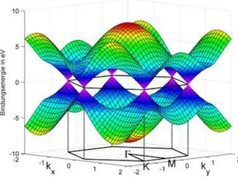
From the main characteristics of graphene, several important properties can be derived; and some of them are, in addition, unique and extreme. Two molecular and delocalized π orbitals perpendicular to the σ ones, have the electrons weakly attached and are responsible for the electronic properties of the system. Most of the properties of graphene are then, related to the electronic band structure,[50] plotted in figure 11. The main characteristic of the electronic band occurs at the Fermi energy (EF), where the π orbitals intersect in six points of two different equivalences, named K and K‟, the so-called Dirac points. The energy dispersion close to the Dirac points is linear with the momentum, being described by E=ħvF. The parameter vF is the Fermi velocity with its value of vF ≈ c/300
(where c is the velocity of light in vacuum), and k is the wave vector.
Figure 11:Electronic band structure of graphene. Dirac cones are plotted where the linear relation between k
and E 51
Close to the Dirac points, electrons (and also holes) behave as massless charge carriers with a speed of 106 m/s (faster than any other material) and a carrier charge density in the order of 1013 cm-2. [52] This explains the very high mobilities predicted and detected in graphene and implies that graphene acts as if it was a semiconductor of zero-gap and like a semimetal, a metal with a negligible density of states at the Fermi level (figure 12).
29
Figure 12: Dirac cones regarding the electronic properties. The cone below is the valence band (electrons), and the above cone is the conduction band (holes)[20]
The electronic band structure of a graphene monolayer, described above, can be modified breaking the symmetry of the crystallographic structure of the graphene sheet.[52] It can be done by stacking more layers, so the energy band in multilayer graphene is different. In addition, as pointed out above, in graphene nanoribbons the band structure depends on the edge geometry and type of termination: armchair or zigzag. (Figure 13)
Figure 13: Armchair and zigzag edges configuration
Coming from its electronic band structure, the most relevant property of graphene is its very high carrier mobility. In graphene, on top of substrates, it is believed that the optical phonon scattering limits the mobility to 120000 cm2/V*s at room temperature. In suspended graphene, the mobility has been shown to theoretically exceed 200000 cm2/V*s at Room Temperature (RT), higher than any known semiconductor.53 Because of the ballistic behavior of graphene, RT Quantum Hall Effect (QHE) and Integer Quantum Hall Effect (IQHE) have been observed in graphene flakes. Interestingly, due to the peculiarities of graphene, we find what is called anomalous QHE, in which the standard sequence of the conductivity with the magnetic field observed in conventional QHE appears shifted in graphene.[54] Another important point about charge transport in graphene is ambipolarity. In the field-effect configuration, this implies that carriers can be tuned continuously
30 between holes and electrons by supplying the requisite gate bias. Under negative gate bias, the Fermi level drops below the Dirac point, introducing a significant population of holes into the valence band. Under positive gate bias, the Fermi level rises above the Dirac point, promoting a significant population of electrons into the conduction band. The access to a truly ambipolar semiconductor enables a number of novel device structures. These are fundamentally different from silicon-based logic because doping levels can be dynamically controlled entirely by gating. Momentarily providing local gate biases to different parts of the same flake can form junctions or even more complicated logic.[55]
Three molecular and strong σ orbitals in trigonal shape are responsible for maximizing the links among the carbon atoms where the hexagonal structure is built (figure 14). The orbitals also provide this structure a great stability. This fact implies a wide range of mechanical, optical and thermal attributes, which are also relevant.[55] Regarding mechanical properties, graphene presents record values like other allotropes of carbon. Harder than diamond, its tensile strength is about 130 GPa (200 times higher than those of the steel) and the Young modulus has been estimated to be in the range of 0.5-1.0 TPa.
Elastic and super flexible, graphene is even very light, weighing only about 0.77 mg/m2.[56] Some works also indicated that graphene has promise as a solid lubricant with thickness on the order of nanometers due to its atomically-thin configuration and high load carrying capacity. When tri-layer graphene is benchmarked with a 2 nm repulsive asperity against an 86% sp3 content diamond-like-carbon (DLC) coating of the same thickness (1.0 nm), the graphene supports up to 8.5 times the normal load of DLC during indentation, and up to twice the normal load of DLC during sliding even after failure of one or more layers. In optics, the main characteristic is the strong light absorption for one monoatomic layer (around 2.3% for visible) but that, in global terms, makes it almost transparent. It can be demonstrated that the absorbance is the result of multiplying πα for the number of graphene layers, where α=e2
/ ħc is the fine-structure constant. This linearity has been demonstrated for up to 5 layers,[39] and it is further confirmed that such unique absorption could become saturated when the input optical intensity is above a threshold value, which makes graphene an ideal transparent conductor where optical transparency and low electric resistance are required. Also the thermal properties are relevant. Thermal conductivities in the basal plane of the order of 5*103 Wm-1K-1 have been reported, exceeding the record values of diamond and carbon nanotubes. This superb thermal conduction property of graphene is beneficial for electronic applications and establishes graphene as an excellent material for thermal management.
31
Figure 14: Scheme of the graphene hexagonal structure and σ and π bonds.39
As a visual and summarized example of some of the properties, we have the “invisible cat hammocks” of figure 15. It claims that an invisible graphene monolayer of 1 m2
would only have a weight of 0.77 mg, and tied between two trees could hold a 4 kg body (e.g. a cat).[53]
Figure 15: A monolayer graphene hammocks placing a cat before breaking.[53]
1.8 Potential applications
The high mobility of graphene makes this material promising for future electronics. The first and main drawback that we have to tackle is the lack of a band gap. In addition, because of the linear dispersion relation, the density of the states in the Fermi energy level does not allow the non-linear response required in electronic applications. It is necessary to substantially modify the conductance when an electric field is applied. Engineering a band gap in graphene samples may be the solution. As it has been explained above, the electronic band structure of graphene can be modified changing the particular structure that has originated it. One of the methods can be functionalizating the graphene surface with other species. Another way is producing graphene nanoribbons. The finite size effects are present in this kind of structures. Also the edges are important. The type of the nanoribbon edge (zig-zag or arm chair) plays a similar role as the chirality does in carbon nanotubes. Moreover, the spin coherence length is also high in graphene which makes it a suitable
32 material for applications in spintronics. If the production methods acquire the sophistication that nowadays semiconducting technology demands, graphene is postulated as one of the main candidates to replace silicon in a hypothetical post-Si era.[55]
The high conductivity combined with the low absorbance of graphene warrants properties required for transparent electrodes. Nowadays the standard material for this purpose, indium tin oxide (ITO), can find a competitor in graphene. Once the growth techniques have been developed, graphene can offer a high quality low cost alternative to ITO in applications such as solar cells, liquid crystal displays and touchscreens. New generation of touchscreens would be in principle possible through very high quality and extremely thin and flexible displays. Due to the high thermal conductivity, graphene-based devices would show less degradation in front of heat and, therefore, have longer lifetimes.
Sensing is another possible field of application due to the extraordinary electronic properties, mechanical resistance and large specific surface area of graphene. The adsorption of molecules in the surface can modify the local charge carrier concentration and this can be detected in a Field Effect Transistor (FET) configuration. A single molecule detection has been achieved, which demonstrates the potential high sensitivity of graphene-based sensors.[57] Sensing is not limited only to chemical species; it can be applied to any phenomena that modify the carrier concentration such as magnetic field and mechanical deformation.
Further application fields that, likely, will be a reality in the near future are:
Ultracapacitors and microbatteries: able to store big quantities of energy, 20 times more powerful than the current ones; and with a charging time 1000 times faster.
Bio-related material: Graphene derivatives, including pristine graphene, GO, chemically reduced GO (rGO) and doped graphene have been intensively studied for their widespread applications in biosensing and detection of biomolecules. Many drugs with beneficial therapeutic properties can also present detrimental side effects, limiting their clinical application. The use of nanomaterials to immobilize and deliver these drugs can assist with preventing undesirable effects. Also, complementary studies are exploring strategies to controllably release the immobilized drugs when the appropriate biological target is identified. The ease by which graphene can be chemically modified seemingly lends itself well to such immobilization and delivery applications.
33
Structural materials (paper, powder): much harder, stronger, and more flexible than current ones.
High performance computation: terahertz oscillators and high-speed field-effect transistors with switching speeds between 100 GHz and a few THz, and a performance 30 times higher than current
Junction diodes: p–n and Schottky diodes are used in a wide variety of electronic/photonic systems as building blocks.
Photovoltaics: more efficient solar cells by using graphene as a charge collector. Electrons in graphene which have been excited to a higher energy state by absorbing incoming light, transfer their energy to neighbouring electrons, rather than radiating it as photons.
Conductive ink: graphene-based coatings for printed electronics (circuits can be printed almost on any substrate) and smart packaging
Graphene based quantum dots: nanolight with extraordinary properties due to their remarkable quantum confinement and edge effects: systematic photoluminescent mechanisms, bandgap engineering, in addition to the potential applications in bioimaging, sensors, etc.
Graphene aerogel: is seven times lighter than air, and 12% lighter than the previous record holder (aerographite). Its density is just 0.16 mg/cm3, and has a superb elasticity and absorption. It can recover completely after more than 90% compression, and absorbs up to 900 times its own weight in oil, at a rate of 68.8 g/s.
Optical modulators: are commonly used in communication and information technology to control intensity, phase, or polarization of light. Graphene allows broadband light-matter interactions with ultrafast responses and can be readily pasted to surfaces of functional structures for photonic and optoelectronic applications.55
Contaminant removal: Graphene oxide is non-toxic and biodegradable. Its surface is covered with epoxy, hydroxyl, and carboxyl groups that interact with cations and anions. It is soluble in water and forms stable colloid suspensions in other liquids because it is amphiphilic (able to mix with water or oil). Dispersed in liquids it shows excellent sorption capacities. It can remove copper, cobalt, cadmium, arsenate, and organic solvents. Recently, graphene shown to be able to remove radioactive nuclides, and heavy metals from water, including radioactive isotopes of actinides and lanthanides. Even at concentrations <0.1 g/L, radionuclide sorption proceeds rapidly.
34
Pressure sensor: The electronic properties of graphene/h-BN (hexagon boron nitride)
heterostructures can be modulated by changing the interlayer distances via applying external pressure, leading to potential realization of atomic thin pressure sensors
Figure 16: (left) Graphene solar cell; (right) a flexible cell phone made of graphene (Samsung) [58]
1.9 Chemically derived graphene
1.9.1 Graphene oxide(GO)
Nowadays, graphene can be produced by micro-mechanical exfoliation of highly ordered pyrolytic graphite (HOPG), epitaxial growth, and chemical vapor deposition (CVD).These three methods can produce graphene with a relatively perfect structure and excellent properties. However in comparison, graphene produced by reduction of graphene oxide (GO) has some important characteristics as it is produced using graphite material by cost-effective chemical methods in large scale. GO consists of a 1D single-layer of graphite oxide and is usually produced by the chemical treatment of graphite through oxidation. It is also highly hydrophilic and forms stable aqueous colloids to facilitate the assembly of macroscopic structures by simple and cheap solution processes. The well-known methods used for the synthesis of graphite oxide are Brodie method,[59] Hofmann method,[60] and Hummers method,[61] and also their modified and improved forms. In these methods, initially graphite powder is chemically reacted with acids (HCl, H2SO4 and HNO3 etc.)
followed by the intercalation of alkali metals (alkali metal compounds KClO3, KMnO4, NaNO3 etc.)
into the graphitic layers which further helps in the breaking of graphitic layers into small pieces. In figure 17 as shown summary of different method‟s
35
Figure 17: Methods for synthesis of graphite oxide using graphite, acids and oxidizing chemicals 62
Compared to pristine graphite, GO is heavily oxygenated bearing hydroxyl and epoxy groups on sp3 hybridized carbon on the basal plane, in addition to carbonyl and carboxyl groups located at the sheet edges on sp2 hybridized carbon (figure 18). Hence, GO is highly hydrophilic and readily exfoliated in water, yielding stable dispersion consisting mostly of single layered sheets (graphene oxide). It is important to note that although graphite oxide and graphene oxide share similar chemical properties (i.e. surface functional group), their structures are different. Graphene oxide is a monolayer material produced by the exfoliation of GO. Sufficiently dilute colloidal suspension of graphene oxide prepared by sonication are clear, homogeneous and stable indefinitely.Therefore, the formation of stable graphene oxide colloids in water was attributed to not only its hydrophilicity but also the electrostatic repulsion.
Also, the structure of GO depends significantly on the purification procedures, rather than, as is commonly thought, on the type of graphite used or oxidation protocol.[62] The exact identity and distribution of oxide functional groups depend strongly on the extent of oxidation. The appearance of chemical composition inside GO and the oxygen containing functional groups in GO can be identified using principally, X-ray photoelectron spectroscopy (XPS) and Raman spectroscopy.
36
1.9.2 Reduced graphene oxide (rGO)
Chemical reduction of graphite oxide is one of the excellent procedures to synthesized rGO and graphene in large quantities. It includes ultrasonication of graphite oxide in water forming a homogeneous dispersion of predominantly soluble GO in water. The GO is reduced by a suitable chemical process; the reduced GO formed resembles graphene but contains residual oxygen and other hetero atoms, as well as structural defects. During the reduction processes, most oxygen containing functional groups of GO are eliminated and the π-electron conjugation within the aromatic system of graphite is partially restored. Finally the rGO gets precipitated from the reaction medium because of the recovered graphite domains of chemically converted graphene sheets with increased hydrophobicity and p-stacking interaction.[64] The properties of rGO are nearly similar to that of graphene prepared through different chemical, thermal, photo, electrochemical or microwave reduction pathways.[65] The most widely applied technique used for preparing chemically converted reduced GO is the chemical reduction of GO as shown in figure 19.[66]
Figure 19: Preparation of rGO by graphite [66]
Fan et al.[67] reported that the exfoliatedgraphite oxide can undergo quick deoxygenation in strong alkali solutions like NaOH and KOH at moderate temperatures (50–90 °C) resulting in stable aqueous graphene suspensions. Figure 20 shows that the addition of NaOH to the graphite oxide suspension led to the change in color (yellow-brown to dark black). Various inorganic and organic reducing agents such as phenyl hydrazine,[67] hydrazine hydrate,[64] sodium borohydride,[66] ascorbic acid,[68] glucose,[69] etc, have been explored for the chemical reduction of GO.
37
Figure 20: a) Illustration for the deoxygenation of exfoliated graphite oxide under alkaline conditions and (b)
images of the exfoliated graphite oxide suspension (≈0.5 mg mL-1) before and after reaction. The control
experiment in (b) carried out by heating the pristine exfoliated GO suspension without NaOH and KOH at 90°C for 5 h with aid of sonication [67]
The GO reduced by heating is known as thermal reduction by annealing. Annealing atmosphere is also important for the reduction of GO. Annealing reduction is usually carried out in vacuum, or in inert or reducing atmosphere. Thermal reduction of GO comprised of the thermal-energy-induced multistep removal of intercalated H2O molecules and oxide groups of carboxyl, hydroxyl, and
epoxy. It should be noted that in chemical reduction, individual GO sheets in the solution phase are chemically reduced by the strong chemical base.[70] The rapid heating of graphite oxide at high temperature, exfoliates in the form of porous carbon materials and get converted into graphene with fewer amounts of oxygen functionalities. The exfoliation occurs by the sudden expansion of CO or CO2 gases evolved from the spaces between graphene sheets during rapid heating of the graphite
oxide. The rapid heating makes the oxygen containing functional groups attached on carbon plane to decompose into gases that create huge pressure between the stacked carbon layers.
1.9.3 Electrochemical exfoliation
One of the most efficient ways of exfoliating graphite is by using strong chemical oxidation, yielding highly soluble, 100% monolayer sheets of graphene oxide (GO). A more tunable, versatile, attractive and principally green approach to drive the intercalation and exfoliation of graphite in solution recently explored is the use of electric fields. Upon using bulk graphite as a working electrode in an electrochemical cell, complete dissolution of graphite can be achieved within a few minutes or seconds, either in water or in organic solvents. By regulating the driving potential in appropriate liquid electrolytes, graphite electrodes can be intercalated with various molecules and

![Figure 18: Structure of GO [63]](https://thumb-eu.123doks.com/thumbv2/123dokorg/7421829.98992/35.892.201.688.107.392/figure-structure-of-go.webp)
![Figure 21: Schematic illustration and photographs of graphite after intercalation, expansion, electrochemical exfoliation and reduction steps (from left to right).[71]](https://thumb-eu.123doks.com/thumbv2/123dokorg/7421829.98992/38.892.97.807.693.1052/schematic-illustration-photographs-intercalation-expansion-electrochemical-exfoliation-reduction.webp)