UNIVERSITÀ DEGLI STUDI DI ROMA
"TOR VERGATA"
FACOLTA' DI INGEGNERIA
DOTTORATO DI RICERCA IN
INGEGNERIA DELLE TELECOMUNICAZIONI E MICROELETTRONICA
XXI CICLO
Design, processing and characterization of organic devices for
optical communications
STEFANO PENNA
A.A. 2007/2008
Docenti Guida: Prof. Aldo Di Carlo, Ing. Andrea Reale Coordinatore: Prof. Giuseppe Bianchi
a Tinozzino
Abstract
The recent explosion of broadband services and the limits imposed by the Moore’s law have stimulated strong research activities towards the integrated optical chips, that are composed of a platform on which many different optical functions, typically in the C‐band, are implemented. Such devices are particularly challenging because integration and compactness play fundamental roles. Among the different materials used to process the optical integrated devices, three main classes can be identified: semiconductors, glasses and organic materials. The last ones are particularly attractive because of the low cost of processing and the high integration related to the amorphous structure, resulting in not required lattice matching conditions.
A common design approach in integrated optics is to optimize a particular optical function with a specific material, then to integrate it on the platform. Among the functions to be implemented, amplification and light generation are still limited with respect to the other functions such as modulation or coupling/splitting. This is due to the limits imposed by erbium for the C‐band operation. Indeed, erbium is difficult to be optically excited because of the small absorption cross section, so host sensitizers such as glasses are needed to efficiently collect the outer excitation and transfer it to the erbium ions. The most famous example of erbium sensitizer scheme
since a long interaction length is required to achieve a sufficient gain level. Erbium‐ doped organic compounds are promising erbium sensitizers for the application to integrated chips as they exhibit attractive features such as high absorption and emission cross section, semiconducting behavior and low cost processing.
The aim of this work is to provide a demonstration of the potential of Er‐ doped compounds for the processing of an electrically driven integrated laser amplifier for the C‐band of the optical communications. The different issues involved in such a challenging device have been studied separately, emphasizing the use of low cost techniques such as solution processing for organic deposition and LED pumping for the excitation of the active compounds. The opportunity for electrical pumping has been demonstrated with the processing of a spin‐coated Er‐doped organic LED. The optically pumped DFB cavities have been fabricated by nano‐imprinting lithography and laser interference lithography and coated by Er‐doped organic compound as active layer, resulting in a narrow emission line centered at 1530 nm. Finally, the waveguide issue has been addressed by designing a channel waveguide. Planar index discontinuity has been achieved by mean of a UV photo‐patterning technique, purposed for the erbium‐doped compound used in this work.
Contents
1. Introduction ... 1 1.1 Integrated Optics: state of the art ... 2 1.1.1 The Monolithic Approach ... 4 1.1.2 The Hybrid Approach ... 5 1.2 Erbium sensitizers ... 7 1.2.1 Ytterbium ... 9 1.2.2 Silicon ... 10 1.2.3 Silver ions ... 11 1.2.4 Organic compounds ... 12 2. Erbium doped organic thin films ... 17 2.1 Erbium tris(8‐hydroxyquinoline) ... 19 2.1.1 Vacuum thermal evaporation ... 21 2.1.2 Solution ... 23 2.1.4 Spin‐coating ... 27 2.1.5 Degradation ... 31 2.2 Enhancement of IR efficiency in Er‐doped organics ... 32 2.2.1 Halogenation of 8‐hydroxyquinoline in ErQ ... 33 2.2.2 Fully halogenation of Er‐doped tetraphenylporphyrin ... 41 3. Organic Light Emitting Diodes for C‐band ... 43 3.1 Working principle of an OLED ... 44 3.2 Design of ErQ‐based OLEDs ... 46 3.3 Solution processing and fabrication ... 48 3.4 Characterization ... 50 3.5 Na[Er(Q57Br)4] based OLED ... 55 4. Organic DFB cavities for C‐band ... 564.3 Processing ... 62 4.3.1 Grating fabrication ... 62 4.3.2 Evaporation of the active layer ... 64 4.4 Characterization ... 65 5. Erbium‐doped organic channel waveguides... 68 5.1 UV‐exposure of ErQ thin films ... 69 5.2 ErQ Channel Waveguide ... 71 5.2.1 Design of the waveguide ... 71 5.2.2 BPM simulations ... 72 Appendix ... 77 Luminescence measurement systems ... 77 Conclusions ... 79 References ... 81 List of publications ... 89 Published Proceedings ... 89 Acknowledgements / Ringraziamenti ... 90
Chapter 1
Introduction
In the 1990’s the worldwide explosion of Internet drastically changed the way people transfer information, allowing all computers on the planet earth to be connected to each other simultaneously. Beside to the sociological and romantic aspects, this meant a strong increase of demand for enhanced information capacities, due to the spreading of broadband services, and so an increase of cumulative demand for higher bandwidth. As a result, two consequences have followed: 1) fibre optics have become the pervasive technology not only for long haul but also for metropolitan communications, replacing the copper‐based interconnects, and 2) new concepts of networking have been developed towards the all‐optical processing of light, extending the use of fibre optics from the nodes to the home line terminations (Fibre To The Home, FTTH).Therefore, a huge increase in the complexity of the optical systems has taken place, from point‐to‐point transmissions to the Wavelength Division Multiplexing (WDM)networking. The optical fibre is a medium with a extremely high bandwidth, about 20 THz, nevertheless today it is impossible to use a laser able to exploit this enormous bandwidth, so multiple single wavelengths laser signals can be multiplexed and transmitted on a single fibre. This is the working principle of WDM, developed in the mid 1990’s. Dense WDM (DWDM) systems with more than 60 wavelengths, each
having 40 Gb/s data, have been demonstrated, so that the total transmission capacity of an SMF is higher than 2.5 Tb/s [1].
In terms of market, there has been a change of philosophy, from the ”bit rate distance product at any cost” challenge of the past [2] to a higher care for cost reduction of the technology in order to bring the optics closer to the customer, according to the FTTx concept. The bottleneck in the deployment of optical networks has always been the availability of low cost components suitable to large scale manufacturing. Unlike electronic components, optical connections needs a good light coupling between fibres and devices, otherwise optical power losses occur making the performances unacceptable. Integrated optics is given to be the key to meet these requirements, allowing to handle the increased complexity of the WDM optical systems and keeping the cost of technology low in order to enable the massive implementation of FTTH.
1.1Integrated Optics: state of the art
There are many slightly different definitions for Integrated Optics (IO), but all of them agree on stating that a Photonic Integrated Circuit (PIC) is an opto‐electronic device that implement all of the main optical functions on a single chip [3].Typically PICs operates at wavelengths in the visible and near infrared range, from 400 nm to 1650 nm.
Two basic issues must be considered in IO and put in evidence the big differences with integrated electronics: (1) the light in a PIC must be confined inside a waveguiding structure to enable propagation of the optical signal all along the chip and (2) the different functionalities must be integrated on the same device with the mandatory condition of low cost fabrication. “While the electronics industry has been able to squeeze millions of devices onto tiny chips, the photonics industry has struggled to place a handful of devices onto a board! And while microelectronic engineers have been able to create complex systems at throwaway prices, most optical networking products still take the form of expensive point‐to‐point links.” This statement is an excerpt of “The Market For Integrated Optical Products: 2001‐2005” report from “Resources And Market” [4] and depicts the state of infancy of IO in terms of development and actual application with respect to the
corresponding electronic integration. This is partially due to the just recent interest of industries in exploration of the potentials of photonics, with the major companies traditionally focused more on pushing the limits of microelectronics than on developing efficient alternatives. The reason is just the intrinsic lower complexity: microelectronic integration technology allows for a broad class of electronic functionalities to be synthesized from a small set of elementary components, such as transistors, resistors and capacitors. Such a technology that supports integration of these elementary components can be used for many different applications and investments made in its development have a potential payback on a larger market [5]. The higher complexity for photonics lies in the variety of elementary devices: couplers, filters, MUX, lasers, detectors, switches, modulators, among the others, are all devices with different working principles each other and have been reported to be implemented with different materials and technologies, so that integration is a very hard target to be centred. Furthermore, passive integrated optical devices and optical interconnects are significantly larger than their electronic counterparts, so the photonic VLSI is impossible to achieve, at least with the current technological perspectives [6].
Anyway, in the last years a change has occurred, taking IO from the small hi‐ tech university spin‐out companies (Luxtera, Optical Cross Links, Inplane Photonics) to the industrial applied research of the major companies (Intel, Enablence, DuPont, CyOptics, NeoPhotonics). This is due to the needs of the computing industry to keep the pace with the increasing processor performance, driven by the Moore’s Law. So the need is for new solutions of optical interconnects for clock distribution first and for signal processing then. As a benefits, the material science and the technological mastery of design and fabrication of PICs has increased, leading to the definition of two main alternative approaches that differ for choice of materials and basic concepts to achieve the integration. Figure 1.1. Volume manufacturing process of optical polymer waveguided circuits [7]
Beside to optical interconnects, a practical demonstration of the benefits coming from IO can be found in the WDM key‐component, used for commercially available MUX/DMUX: the Arrayed Waveguide Grating (AWG). The AWGs are Photonic Integrated Circuits (PICs) typically formed on silicon substrate. They integrate multiple optical functions on a single substrate leading to a single package, volume manufacturable on a fab that is well developed in the semiconductor industry. Moreover, this technology allows integration of actives and passives on a single substrate leading to further size reduction, efficiency and reliability. An AWG optical chip is composed of input waveguides, an input slab, array of waveguides, output slab, and output waveguides. All of these are fabricated on a single substrate forming an optical integrated circuit. This device represents a deep improvement with respect to alternative solution for WDM MUX/DMUX such as Fibre Bragg gratings and cascaded filters [8].
Before description of the different IO technologies, it must be considered that in the IO area the transmission medium (polymer waveguide or silica fibre), the integration platform (silicon, GaAs, InP, polymer, silica) and the level of integration (monolithic opto‐electronic, monolithic photonic integration with separate electronics, or optical platform with hybrid electronic and optical components) are still a matter of active investigation, so there is not yet a clearly pervasive technology, even if nowadays silicon photonics is able to gain higher funding from industry, thus assuring more resources for R&D.
1.1.1 The Monolithic Approach
The first approach aims to achieve the monolithic integration, implementing the optical functions with silicon. The attractiveness of silicon‐based optics is the potential integration with CMOS integrated circuits for high‐volume manufacturing. The first prototypes of such silicon‐based optical components includes several basic functions on a single silicon chip, such as a thermally tunable WDM Bragg filters, high‐ speed optical MZI modulators and a Si/Ge high‐speed photodiode [9] or a continuous‐ wave Raman silicon laser [10] that exploits the Stimulated Raman Scattering (SRS), in which sub‐bandgap photons interact only with phonons. The last work, from people at Intel, is particularly impressive, even if it has not a practical use (optical excitation required, small spectral range of wavelengths for optical gain [11]), because achieving optical gain and/or lasing in silicon has always been one of the most challenging goals in silicon‐based photonics: bulk silicon is an indirect bandgap semiconductor, resulting
in radiative (light emitting) decay being less likely compared to other non‐radiative (e.g., Auger recombination) routes, and thus in a less‐efficient corresponding light emission [12]. Furthermore, there is a mismatch between silicon band edge luminescence at 1100 nm and the requirement to operate at wavelengths around 1550 nm for full compatibility with fibre optic communications systems. So, light emission in silicon has traditionally focused on the use of silicon engineered materials such as doped nanocrystals [13], Si/SiO2 superlattices, erbium‐doped silicon‐rich
oxides [14], surface‐textured bulk silicon and Si/SiGe quantum cascade structures [15]. The flaw of such a monolithic approach lies in the difficulty to implement all the optical functions meeting at the same the high performance expectations required.
1.1.2 The Hybrid Approach
A completely alternative approach is based on the consideration that, as previously noted, optical components such as tunable WDM filters, photodiodes, optical waveguides are all devices optimized with different materials and technologies, precluding them from an easy optoelectronic monolithic integration. Therefore, a valid method to achieve high performance at the lowest possible cost is the choice of the most appropriate material for each function on one side and the parallel development of an integration‐friendly platform on the other side, resulting in a different method [3]. This is the so‐called hybrid approach, that comprises also amorphous materials, such as polymers, that are free from restrictions related to the lattice matching condition of the crystalline structures. Figure 1.2. Device structure of a hybrid silicon evanescent PIC [15]
A first hybrid approach makes use of III‐V compounds, commonly used for electroluminescence and lasing in the telecommunications windows, aligning and bonding pre‐fabricated III‐V active devices to individual waveguides fabricated on a silicon platform. This approach has the benefit of using electrically pumped active devices on a silicon platform, but since the III‐V devices are aligned and bonded individually, the time and cost of manufacturing limits the total number of lasers that can be bonded on a single wafer. Moreover, limited alignment accuracy causes coupling loss variation and large reflection between the III‐V active devices and the silicon waveguides. As alternative for III‐V compounds, the device can be grown on silicon platform [16]. This approach is compatible to silicon and, moreover, allows for electrical stimulation, but the manufacturing procedures are complex and expensive, so the key requirement of low cost manufacturing can difficultly be met.
Many different optical technologies have been demonstrated including polymer waveguides integrated on Si, planar light wave circuit interconnects and fibre ribbon arrays integrated with VCSELs and photodiodes. Polymer waveguides are selected because of their potential for high‐volume, low‐cost production. For instance, the acrylate‐based (PMMA) multimode polymer waveguides are known for their low loss (0.08 dB/cm), ease of integration, best system performance and manufacturability [17][18]. Polymers can be made photosensitive and as such can be directly photo‐patterned and wet‐etched with a solvent, speeding the fabrication cycle time to tens of minutes per multi‐layer optical circuit on a wafer. These materials have an obvious throughput advantage in production [3]. Beside to waveguides, that today gain the most of interest from industry for the chip‐to‐chip interconnects, polymers and organic materials in general have been demonstrated to be efficient materials for several optical devices, like EO modulators [19], detectors [20] and amplifiers [21].
Other amorphous materials than organics are used for IO devices, like sol‐ gels, that are used for low cost processing of Bragg reflector waveguides, exploiting the UV‐induced tuning of the sol‐gel refractive index (over a range of 0.1) to obtain the proper index profile for light confinement [22]. In addition, sol‐gel based IO devices integrating modulators, tunable filters and switches have been reported [23].
Doped glasses are another alternative solution for waveguided IO devices [25] that has already met the commercial availability, with some examples of Erbium Doped Waveguide Amplifiers (EDWAs) manufactured at Teem Photonics [24].
Finally, ceramic oxides like alumina (Al2O3) that incorporate active materials
(see 1.2) have also been used for efficient waveguiding amplifiers [21].
Figure 1.3. An Ion‐Exchange planar glass waveguide from Teem Photonics [24]
1.2 Erbium sensitizers
One of the critical issues in IO is the need for compensation of loss, mainly due to absorption and scattering inside the device and to the light coupling among devices, that can make the performances unacceptable. So, a great interest is focused on the active materials and solutions that can be integrated on a waveguide. Furthermore, these active materials can be used for implementing the functions of signal generation and amplification on the integrated platform, mostly in the 2nd and 3rd optical communications standard windows, centred respectively at 1310 nm and 1550 nm. As previously mentioned, III‐V compounds can be used to have light generation in these ranges, but they take disadvantages due to the expensive manufacturing technologies involved in III‐V compound processing.
Therefore, a valid alternative is represented by some Lanthanide elements, the so‐called Rare Earths (RE), whose optical transitions lie in the ranges of interest for IO, mainly Erbium, Neodymium and Ytterbium. To process a device entirely with such materials would be extremely expensive, hard from a technological point of view and finally inefficient because the optical transitions in the free ions are parity forbidden [26]. Nevertheless, these materials can be incorporated in host materials that can act as sensitizers. Erbium doped materials have attracted a big interest because of their unique emission properties ideal for IO, related to the 4I13/2 Æ 4I15/2
transition near 1540 nm wavelength that matches the lowest‐loss window in optical fibre systems. The erbium trivalent ions (Er3+), that is the favourite bonding state of erbium, shows an intra 4f shell transition from its first excited state 4I13/2 to the
ground state 4I15/2 which results in the near infrared light emission at 1540 nm [27]. In
the pure Er3+ ions this process is parity forbidden because the energy levels of the 4f shells have equal parity. However, if erbium is incorporated in a solid host, the transitions become weakly allowed because the wave functions of the electrons are in
some way “disturbed”. Because the transition is an atomic dipole, the absorption and emission cross section for the optical excitation are quite small ( 10−21 cm2) and the lifetimes of the luminescence are quite long, in the order of 1 ms [11][26][27][28]. Moreover, erbium ions in a solid are influenced by the electric field that removes the degeneracy of the 4f levels, resulting in a Stark‐splitting of the energy levels, so that manifolds arise instead of sharp levels [29]. Due to the outer shell shielding, the magnitude of the splitting is small, resulting in relatively narrow lines of emission that are independent of the host material.
The most representative application of erbium in photonics is the Erbium Doped Fibre Amplifier (EDFA) [30] that is composed of a glass fibre whose core is doped with erbium ions. EDFAs can be efficiently optically pumped by a 980 nm or 1480 nm emitting laser to get the right population inversion. EDFAs are the current pervasive technology for optical line amplification. However, this technology presents some features that make it unsuitable for IO. First, the size: to get enough amplification, a long fibre cable is needed (typically in a 10 ‐ 40 m range) because erbium concentration in the glass host is limited by quenching effects, such as ion‐ion interactions, that convert the pump photons into heat. In addition, the issue of erbium clustering in silica must be considered since it is sensitive to composition and exacerbates the cooperative processes (cross relaxations and up‐conversion) [31]. The other main flaw is the cost. An EDFA is an expensive device mostly because it requires an accurate high power pump laser (10‐100 mW) [27] to excite efficiently the narrow lines of erbium absorption. So, EDFAs can’t meet the requirements for low‐cost and compact devices of integrated photonics.
To avoid the use of lasers and reduce the interaction length of the active medium a different approach is required. Erbium sensitization can play an interesting role in this context for the realization of EDWAs (Erbium Doped Waveguided Amplifiers). A sensitizer coupled to an Er ion can absorb pump photons with a much larger than erbium cross section and then it can transfer the energy to Er. If the sensitizer has a broadband absorption spectrum it may be pumped by a broadband source such as a LED, much cheaper than a laser (from 2 to 3 orders of costs). In such a case, by choosing the proper pump wavelength, one of the limiting factor to gain in erbium doped materials, the Excited State Absorption (ESA) may also be avoided [27]. In this paragraph, a deeper discussion on the different schemes available for Erbium sensitization is presented, showing how the integration approaches are still valid at this level and allow for a wide choice of solutions with different performance and cost requirements.
Figure 1.4. Absorption spectrum of Erbium doped silicate glass [31]
Currently there are four schemes available for erbium sensitization: (1) Ytterbium, (2) semiconductor (typically Silicon) nanocrystals and nanoclusters, (3) metal ions and (4) organolanthanide compounds.
1.2.1 Ytterbium
The ytterbium ion (Yb3+) shows a 980 nm‐peaked absorption band that is almost resonant with the erbium band 4I13/2. The absorption band of Yb3+ at 980 nm is
quite wide, thus Yb3+ can be excited by a broad band source in the range 850 nm – 980 nm. Since the absorption cross section of Yb3+ at 980 nm (10‐20 cm2) is tenfold the one of erbium, Yb3+ can efficiently absorb the pump radiation and transfer it to Er3+, resulting in a several times more efficient excitation of Er3+ than the direct excitation of Er3+ [27]. In addition, ytterbium is a two‐level system that is not affected by upconversion between the ions [32]. A disadvantage of such sensitization scheme lies in the reversibility of such a process due to the energy backtransfer from erbium to ytterbium. Another flaw is the limited concentration of Yb. Indeed, over a threshold limit that depends on the waveguide cross section, the upconversion coefficient and the ESA cross section, the ytterbium concentration is countereffective as it causes a poor improvement in gain with respect to the only Er doped waveguide, due to the effect of the large absorption of Yb [27].
Anyway ytterbium is currently often used as co‐dopant for instance in Er‐ doped polymer waveguide amplifiers [32] and Er‐doped phosphate glasses [33] as it
contribute to enhance the effective pump‐absorption cross section of Er3+ ions resulting in an improved photoluminescence efficiency.
1.2.2 Silicon
Bulk semiconductors are naturally efficient sensitizers for rare earth ions. When RE ions are incorporated inside a semiconductor, they act as point defects that introduce defect levels in the semiconductor bandgap, enabling the generation of traps for the optically or electrically induced carriers. The trapped carriers can generate a bound exciton and, according to the impurity Auger process, can recombine by energy transfer to the RE ions exploiting the strong spatial overlap. Like Yb3+‐Er3+ sensitization, in this case the process is reversible, too, with the quenching of the infrared emission of erbium due to the generation of an exciton induced by the strong exciton‐Er coupling. The energy backtransfer has been proved to be highly effective at room temperature [34]. Indeed, erbium‐doped silicon waveguides have shown infrared light emission when the silicon is co‐doped with oxygen to produce optically active ions in the lattice [35]. A PN junction can be formed and the erbium ions can be pumped electrically to give electroluminescence [12]. Unfortunately, although emission can be relatively strong below 100 K, the emission intensity falls rapidly when the device is heated to room temperature [34].
A solution for such an undesired process is to increase the bandgap in the bulk silicon in order to make the backtransfer less probable on one side and to decrease the coupling erbium‐excitons on the other side. To achieve the first target, the silicon bandgap can be enhanced by co‐doping with oxygen [27] and processing the Silicon in such a way that Si nanocrystals [36] and/or nanoclusters [37] (Si‐nc) generate within the silica matrices. The second target can be centered optimizing the Er‐exciton coupling within the silica matrix that is dependent on the spatial separation between the nanocrystal and Er. Therefore, the coupling depends on the erbium concentration: typically, the higher the concentration , the lower is the nanocrystal luminescence, but at the same the lower the concentration, the lower is the Er‐ exciton backtransfer. It has been demonstrated that the proper level of erbium concentration is within a range of 0.02% ‐ 0.04% weight [27].
These structures have showed many properties that make them optimum sensitizers. Indeed, silicon nano‐crystals suspended in silicon‐rich oxide restrict carrier movement while still allowing electrical pumping [38]. In terms of performances, the effective excitation cross section of the Er3+ 1.54 μm peaked luminescence broadens and strengthens up to values of 10‐16 cm2 under visible light pumping, with quantum
efficiencies greater than 60% by pumping at 488 nm. In addition to the increase of excitation cross section, Si‐nc increase the average refractive index of the dielectrics, allowing good light confinement for waveguiding, and conduct electrical current, which enables the electrical pumping of optical amplifiers [37]. These structures are affected by strong detrimental phenomena such as cooperative upconversion and confined carrier absorption.
Recently, a LED pumped Er‐doped nc‐Si/SiO2 silica micro‐amplifier (amplet)
has been reported [39]. This represents an important goal in the definition of low cost and compact waveguided devices for integrated photonics.
However, expensive and high consuming manufacturing techniques are involved in the processing of Silicon nano‐particles, such like RF sputtering, ion implantation, aerosol synthesis, chemical vapour deposition and reactive evaporation of silicon rich oxides [11]. Indeed, high temperature thermal curing is required to form silicon nano‐clusters (750 °C) and nano‐crystals (1100 °C).
1.2.3 Silver ions
When incorporated in a glass, silver has been demonstrated to be a good sensitizer for erbium, since it has shown several absorption and emission bands in the visible and near ultraviolet ranges [27] that can be resonant with erbium manifolds. Silver doping of glasses is commonly achieved by ion exchange, a cheap and well performing technique [40], wherein network modifiers of the glass such as Na+, K+ are interchanged with the silver ions [27]. In such a way a good index discontinuity can be obtained to process waveguides on glass substrate [41].
Recently, a single‐end pumped waveguide laser based on Er:Yb‐doped phosphate glass has been realized, showing an output power higher than 20 mW with a 17% efficiency at 1533.3 nm. Although their absorption cross section is low if compared to nc‐Si (10‐20 cm2 for 980 nm pump band [42]), phosphate glasses can be heavily doped. For such a reason they are preferred to silica glasses wherein erbium concentration is limited by quenching effects in silica. Indeed, as previously mentioned, highly doped material is required to meet the demand of high‐power together with a compact laser cavity (in the order of few cm). Furthermore, phosphate glass also makes co‐doping with Yb3+ ions more beneficial for pumping in view of higher phonon energies in the phosphate, resulting in efficient energy transfer from Yb to Er [43].
In such a way, phosphate glasses allow to achieve higher efficiency of emission at 1550 nm, and so the interaction length of the device, particularly critical for integrated optics, can be reduced [44]. Figure 1.5. Layout of a laser chip fabricated on Er‐Yb codoped glass substrate [41] Nowadays, glass integrated optics seems to be a good compromise between semiconductor lasers and optical fibre lasers. Semiconductor lasers exhibit a high emission wavelength sensitivity to external noise sources such as temperature. On the other hand, optical fibre lasers show very good stability but are cumbersome, making integration extremely complicated. Furthermore, glass devices requires lower temperatures for vacuum thermal annealing (350°C) [27].
1.2.4 Organic compounds
Erbium doped organic compounds have gained attention because of their appealing features as low cost, ease of fabrication on a wide range of substrates, low dispersion and broad luminescence bands. Polymer amplifiers can be integrated into existing optical polymer devices already demonstrated (and in some cases, commercially available), such as switches [45][46], splitters [47] and MUX [48], with low coupling losses.
Furthermore, the opportunity of organic synthesis allows for “tailoring” of molecules, i.e. the engineering of the materials for the control of various optical parameters such as refractivity, birefringence, thermal stability, among the others, important to proper design and realize a waveguiding device.
As mentioned, polymers have the advantage to be deposited by low cost solution‐processing techniques such as spin‐coating in room temperature conditions. The subsequent thermal annealing rarely is higher than 200 °C. Indeed, temperatures higher than 110 °C can be detrimental for some organics like polymers.
Inorganic erbium compounds such as erbium salts (e.g. erbium chloride) cannot be used as rare‐earth sources in polymer matrix as they cannot be solvated by organic solvents. However, Er ions can be incorporated in an organic ligand to form an organolanthanide molecule that can be easily dispersed in a polymer film such as poly(methyl‐methacrylate) (PMMA) [49] or poly(phenyl‐methacrylate) (PPMA) [50] and in sol‐gels [51][52]. In addition, the polymer matrix can act as sensitizer of the ligand, enabling a double steps excitation mechanism, as suggested in [50]. This ligand must provide enough coordination sites in order to bond to the erbium ion in a stable complex [27] and to shield the ion from the neighbours and from impurities in the polymer matrix that may quench the near IR fluorescence.
In organolanthanide complexes erbium can be directly excited, nevertheless the great advantage is that organic can be excited, too, resulting in a several times more efficient excitation. Indeed, the organic ligand acts as sensitizer for erbium, according to the Antenna effect [53] showed in Figure 6 and described here in the following. Figure 1.6. The Antenna effect in an organo‐erbium system
Figure 1.7. Sensitization scheme and energy transfers of an organolanthanide guest in a polymer matrix [54]
Typically, the organic complex acts as an “energy antenna”, being efficiently excited from the singlet S0 ground state to the singlet S1 excited state. This is followed
by fast relaxation to the triplet T1 state and from there energy transfer to one of the
Er3+ 4f levels may take place. From these levels, rapid relaxation to the 4I13/2 first
excited state in Er3+ takes place. Finally, the Er3+ may decay to the 4I15/2 ground
manifold resulting in the emission of a 1530 nm photon [27].
Er3+ ions in the organic complex have been reported to have an absorption cross section in the order of 10‐20 cm2, one order higher than the free Er3+ ions [27]. Unfortunately, short lifetimes (in the order of 100 ns) of luminescence have been observed, likely due to the quenching effect of water residuals within the molecule that coordinate with erbium [27][55]. It is known that OH groups are detrimental for near infrared absorption around 1420 nm, corresponding to the first vibrational overtone of the OH bounds. For instance, this led to the definition of the 2nd and the 3rd windows of telecommunications, just around the O‐H related absorption peak in the silica fibres. For erbium ions, which exhibits a strong interaction with water, the same occurs, since the overtones of the OH groups positioned close to the erbium ion (1 nm) are resonant with the 4I13/2 Æ 4I15/2 transition [27].
Therefore, the short luminescence lifetimes requires for high pump power to get the proper population inversion. This flaw can be compensate by the high absorption cross section showed by the aromatic component of the organic ligand, whose value is in the order of 10‐18 ‐ 10‐17 cm2. The wide absorption band of the ligand typically lies in the ultraviolet range, with some cases reported in the near UV [56]. In this last case, the use of wide emission sources such like LEDs as pump sources is enabled, as shown in the next chapter.
With respect to infrared luminescence spectra observed for erbium coupled to the other sensitizers, the erbium‐doped organic compounds show much wider spectra, with a spectral width (FWHM) of up to 80 nm [57]. The huge broadening of IR luminescence can be assigned to the coupling of the vibrational modes of the organic ligand with the 4f‐4f electronic transitions of erbium, as expected [49]. This feature candidates such compounds as active materials for optical amplification, mainly in the C‐band (1530 nm‐1565 nm), but also in the neighbor S‐band (1460 nm – 1530 nm) and L‐band (1565 nm – 1625 nm). Furthermore, broad spectrum sources induce a lower ESA on the erbium ion, resulting in a better quantum efficiency [27].
The basic quantum yield of organolanthanides is low, in the order of 10‐4 [50]. Besides to the previously mentioned OH group quenching, these low efficiencies are also associated with the high‐frequency CH vibrational bands of the organic ligands that couple with the Er3+, reducing the lifetime of the emitting level by multiphonon relaxation at microseconds, whereas it should be 3 orders of magnitude higher (4 ms). In order to achieve more efficient luminescence from lanthanides, and thus a higher quantum yield, it is necessary to complex the ions with a ligand functionalized by a chromophore that optimize the energy harvesting, in some cases shifting the absorption peak in the visible range of wavelengths, wherein cheaper and commercially available sources are available [50][57]. In such a away, 10‐3 efficiencies can be achieved [50]. Recently, a erbium thiolate (DME)2Er(SC6F5)3 has been
demonstrated [58] to give 75% efficiency with luminescence lifetime of 2.88 s, very close to the 4 ms upper limit identified for erbium‐doped organic compounds [27]. This impressively huge efficiency is attributed to the absence of direct Er coordination with fluorescence quenching vibrational groups such as hydrocarbon and bonding of hydroxide groups. Indeed, there are no OH functionalities, and the limited number of ligands with CH bonds are connected to the Ln through weak dative interactions, rather than covalent bonds between the metal cation and a hydrocarbon chain or hydroxide ion. In both complexes, Er ions are bound to heavy elements such as S, Se, I, and fluorinated thiolates, and because of the proximity of such heavy elements and fluorinated organic functionalities, high fluorescence quantum efficiency is achieved.
Up today, the most popular erbium‐doped organic complexes, that have provided good results when used in devices, are: erbium‐tetraphenylporphyrin (ErTpp)acac that has been demonstrated to be efficiently dispersed in several polymers like MEH‐PPV [57] and poly(arylene–ethynylene) (PAE) [58] to give electroluminescence, Er‐doped polydentate hemisperands that have been reported to be used for polymer waveguiding amplifiers as dispersed particles in PPMA [27][50], whereas tris(dibenzoylmethanato)(monobathophenanthroline) erbium(III) complex
[Er(DBM)3] [59], erbium tris 8‐hydroxyquinoline (ErQ3) [60], erbium (III) 2, 4‐
pentanedionate (Er(acac)3) [61] and tris(acetylacetonato)(1,10‐phenanthroline)
erbium [Er(acac)3(phen)] [62] have been reported to be used as active layers in
electrically stimulated Organic Light Emitting Diodes (OLEDs), as it will be shown in the chapter 3. Figure 1.8. Some erbium‐doped organic molecules [56][57][58][59]
Chapter 2
Erbium doped organic thin films
Thin film deposition of organic materials is a basic step in the processing of organic devices because a careful control on the thickness and the quality of the organic layer must be performed. Indeed, charge transport between molecules and exciton generation and recombination are mechanisms that are strongly affected by the presence of undesired impurities or not ordered roughness in an organic active layer. The low thickness values involved, in the order of 10 nm up to 100 nm, make the process control a critical issue.
Depending on the type of organic material, different deposition techniques are used. Small molecules, i.e. monomers or oligomers, that are light molecules with strong bounds and high melting point, are typically deposited by vacuum processing techniques, mainly vacuum thermal evaporation, which involves high temperatures (200 °C – 300 °C). Polymers, that are heavy molecules made of long chains of monomers, usually cannot be processed at temperatures higher than 110 °C as degradate before melting, losing the properties they are synthesized to. However, polymers can be easily solvated in solutions and deposited by room temperature solution processing techniques such as spray‐coating, spin‐coating or ink‐jet printing. Then, thermal annealing at the boiling temperatures of the solvents, lower than 110 °C for most of organic solvents, is performed. Although vacuum thermal evaporation allows for a more controlled, accurate and impurity‐free deposition, solution processing represents the key factor for the success of polymers in optics and
electronics because fast, simple and extremely cheap processing, mostly with respect to semiconductor’s industrial techniques, can be used [3], meeting the requirements of the integrated optics for low cost, as mentioned in the former chapter.
Erbium‐doped organolanthanides are small molecules, so they are naturally compatible to vacuum thermal evaporation. Nevertheless, in order to exploit the edges of solution processing, big efforts have been made to make these molecules easily and efficiently dispersed in polymer matrices to get a guest‐host system [29][57].
In this work two types of erbium doped organic materials, erbium tris(8‐ hydroxyquinoline) [ErQ] and Er‐tetraphenylporphyrin acetylacetonato [Er(TPP)acac] has
been mainly studied. Nowadays ErQ is the most appealing organic IR emitter because it has been demonstrated to be electrically stimulated to give IR electroluminescence from an OLED [63]. In addition, opportunity for dispersion in mesoporous silica [51] has been reported. Therefore, since few years ErQ is the only commercially available organo‐erbium compound (Sigma Aldrich, Gelest, ABCR).
In order to exploit both solution processing advantages and ErQ benefits for 1550 nm emission, in this work a great effort has been made to solvate the ErQ and deposit it by controlled spin‐coating. To evaluate the effects of the different deposition techniques on the ErQ optical properties (absorption and luminescence), thermal evaporation of ErQ has been performed and optimized.
This chapter presents the results related to the evaporation and the purposed spin‐coating technique, developed to achieve a good quality deposition of ErQ thin films with 40 nm – 60 nm thickness. The same technique has been used to process an enhanced version of Er(TPP)acac thin films. Results of optical characterization of the
solutions and the thin films is reported.
Finally, in order to reduce the C‐H bonds‐related quenching of IR emission and improve the quality of solution processing, halogenation of the two materials has been performed. Results on effects and improvements of such a study are reported in the end of the chapter.
It should be noted that ErQ has been optically characterized in form of powder, solution, drop‐cast film, evaporated thin film and spin‐coated thin film. This characterization has been aimed to verify possible variations of the optical properties depending on the state and the deposition technique used for the material. Absorption spectra have been detected with a Varian Cary 50 UV‐vis spectrophotometer in a quartz cuvette. Luminescence has been detected by the spectroscopy set‐up reported in Appendix A.
2.1 Erbium tris(8-hydroxyquinoline)
Erbium tris(8‐hydroxyquinoline) (ErQ, CAS number 23696‐16‐8, formula C27H18ErN3O3), also named as tris(8‐hydroxyquinolinato) erbium (III), is an
organolanthanide molecule composed of three Quinoline groups coordinated to a trivalent erbium ion Er3+ (see Fig. 2.1). Recently, a trinuclear structure Er3Q9has been
proposed [64], in which the Er metals are fully coordinated by the quinolinolate(Q) ligand molecules.
Besides to be an efficient sensitizer for erbium, Quinoline is also a popular organic semiconductor [4], used for charge transport properties in other organo‐ metal compounds such like Aluminum Quinoline (AlQ3) that is commonly used as
electron transport layer and green emitter in OLEDs [65]. Figure 2.1. 2D and 3D pictures of an ErQ molecule
The sensitization scheme of ErQ accords to the Antenna effect resumed in figure 2.2 that also shows the energy values involved in the process: (1) absorption of a photon induces an excited singlet state on the Quinoline, (2) intersystem crossing from the excited singlet state to a triplet state, enhanced by the heavy atom effect, may occur, (3) intra‐molecular energy transfer from the triplet state of the ligand to one of the excited 4f states of the lanthanide ion via a Dexter transfer mechanism takes place and finally (4) intra‐4f transitions within the Er3+ produce IR luminescence. It must be observed that, differently from other rare earth quinolines wherein the triplet decay is strongly dominated by radiative decay (phosphorescence) with a characteristic visible emission at 600 nm, in ErQ the triplet decay is dominated by energy transfer to energetically resonant states of the erbium ion, mainly 4F9/2 as
reported by many study on the subject [66][67], as suggested by the spectral overlap between Er3+ absorption and the ligand emission reported in [68].
Figure 2.2. Sensitization and photoluminescence scheme of ErQ [69]
A typical absorption spectrum of ErQ is shown in figure 2.3, with a near ultraviolet (NUV) peak at 380 nm and a second lower peak at 325 nm. As previously mentioned, these peaks are related to the Quinoline that efficiently harvests the light excitation. This is consistent with what reported in previous publications [66], with the 380 centered band having a great spectral portion in the visible range. This band represents one of the big edge of this compound, since it enables the excitation by commercially available visible sources, as reported in [56]. The 325 nm secondary peak has been attributed to a vibronic progression due to the ring deformation modes [70].
Luminescence measured on ErQ powder in figure 2.4 showed the typical emission of the 4f‐4f transition at 1535 nm. The spectral width (FWHM) value is 80 nm, from 1490 nm to 1570 nm. This is a much higher value than what reported in other erbium doped hosts, as discussed earlier.
The ErQ used for experiments has been selected from three different batches: a first batch from a lab‐made powder coming from Queen Mary University of London (Dept. of Physics, Prof. W. P. Gillin), a second one from Gelest Inc. (purity > 95%, product number AKE276), a third batch from Sigma‐Aldrich (purity > 97%, product number 658502). A common behavior in terms of absorption and infrared emission has been observed, instead the visible emission has been observed to be different in some cases, as it is reported in the following sections.
300 350 400 450 500 550 600 650 0,0 0,1 0,2 0,3 0,4 0,5 0,6 0,7 A b s o rbanc e ( O pt ic al den s it y ) Wavelength (nm) Figure 2.3. UV‐Vis Absorption spectrum of ErQ powder Figure 2.4. Excitation (PLE) and IR emission (PL) spectra of ErQ powder (ErQ is identified as Er1)
2.1.1 Vacuum thermal evaporation
Vacuum Thermal Evaporation (VTE) is the basic deposition technique for small molecules such as ErQ that exhibit a melting point at temperatures lower than degradation point, thus tolerating the high temperature involved in the process. ErQ has a melting point floating from 280 °C to over 300 °C as reported by producers [Sigma Aldrich, Gelest]. However, evaporation of uniform thin films is not an easy task
to complete, nor evaporation parameters of the material, such as weight density and Z‐ratio, are known. Therefore, several tries have experimented to control and optimize the process. Evaporations have been performed with a on borosilicate glass and silicon dioxide substrates, enabling the spinning of the sample‐holder to achieve a more uniform deposition. It has been found that selecting evaporation parameters as in the following: ‐ weight density: 1.55 g/cubic cm ‐ z‐ratio: 1 ‐ tooling: 200 (specific for evaporation system) ‐ chamber pressure before evaporation: 7.4 x 10‐7 mbar In such a way an accurate control has been achieved with a typical mismatch between the nominal and actual thickness values in the order of 0.3%. Figure 2.5 shows the step of the thin film on the substrate: the missing of particles on the layer emphasizes the quality of the process. Figure 2.5. Surface profile of ErQ thin film (780 nm) on Silicon (100) wafer Optical characterization performed on the evaporated thin films in the visible range, showed in figure 2.6, resulted in a 525 nm centered spectrum that is consistent with previous publications [63][68]. This peak is related to the ligand singlet emission. Typically, in many lanthanide‐quinolinate compounds such as YbQ a 600 nm peak is also observed, related to the triplet radiative emission. The absence of this peak in ErQ demonstrates the efficiency of the triplet‐to‐ion energy transfer, that dominates on the radiative deactivation of the triplet [68].
400 450 500 550 600 650 700 750 0,0 0,2 0,4 0,6 0,8 1,0 No rm alized Inten s ity Wavelength (nm) Figure 2.6. Visible photoluminescence of an ErQ thin film deposited by VTE 1400 1450 1500 1550 1600 1650 1700 0 50 100 150 200 250 300 350 400 450 500 550 P L I n te n s it y (a .u .) Wavelength (nm) Figure 2.7. IR photoluminescence of an ErQ thin film deposited by VTE The infrared luminescence spectrum in figure 2.7 showed the typical erbium‐ related 1535 nm peak. The side peak at 1490 nm is due to the side emissions of the 4I 13/2 manifold as an effect of the Stark splitting [55].
2.1.2 Solution
Although several publications [71][72] and producers [Gelest] report about ErQ as dissolvable in common solvents such like methanol and chloroform, it has not
been confirmed by direct experience. Instead, Dimethyl Sulfoxide (DMSO) and Dimethylformamide (DMF) have been experimented to be the only effective solvents on ErQ. For safety, DMSO has been selected as working solvent. To allow for the spin‐coating deposition of a layer as thicker as possible, the limit concentration of ErQ in DMSO has been searched for. The limit, identified as the threshold which the solution turns to opaque over, has been found to be 4% weight. Figure 2.8. ErQ solution in DMSO at 4 % weight 350 400 450 500 550 600 650 700 750 800 0,0 0,2 0,4 0,6 0,8 1,0 Absorbance ( a .u .) Wavelength (nm) Figure 2.9. UV‐Vis Absorption of ErQ solution in DMSO
Absorption characterization performed on ErQ solution in a quartz cuvette gave a spectrum (see figure 2.9) with a peak at 520 nm that can be related to the 4f11 manifold in the erbium ion (population of the 2H11/2 level) [67][73], besides to the
known peak of the ligand at 380 nm.
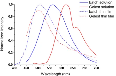
As previously mentioned, the visible luminescence shown in Fig. 2.10 strictly depends on the batch of material under characterization. In particular, the lab‐made batch (in figure, ErQ batch) has the typical peak related to the singlet emission, even if slightly red shifted at 565 nm with respect to the usual ErQ emission at 525 nm. Furthermore, a 595 nm side peak can be observed. The solution based on the
commercial compound instead features an unexpected behaviour with two peaks at 618 nm and 664 nm, that are reported for ErQ powder [72] and the ErQ‐based evaporated OLED by Gillin [63]. Emission at 600 nm is associated to triplet emission in Quinoline [66], but it has never been observed in ErQ because most of triplet decay is routed towards energy transfer to erbium resonant manifolds rather than towards phosphorescence (triplet emission). It should be noted that in the evaporated thin film, for both the batches, only the 500 nm peak can be observed, as reported in figure 2.11 for a comparison, so the unexpected emission of Gelest compound could be explained by effects of the DMSO on the molecule. 450 500 550 600 650 700 750 800 0,0 0,2 0,4 0,6 0,8 1,0 In ten sity Wavelength (nm) ErQ batch ErQ Gelest Figure 2.10. Visible luminescence of ErQ solution in DMSO at 4 % weight
400 450 500 550 600 650 700 750 0,0 0,2 0,4 0,6 0,8 1,0 No rm al iz ed In te n s it y Wavelength (nm) batch solution Gelest solution batch thin film Gelest thin film
Figure 2.11. Comparison of visible luminescence of ErQ solution in DMSO (4 % weight) and evaporated thin films for two batches of ErQ
A possible further explanation could be found in the low purity of the commercial ErQ powder, 95% for Gelest batch, whereas lab‐made batch is supposed to have an higher degree of purity (typically 99,99%), but it is not enough to explain the absence of the traditional singlet emission in the green range. 350 400 450 500 550 600 650 700 750 800 850 0 500 1000 1500 2000
2500 ErQ casting visible PL ErQ casting visible PL (UV filtered)
In te nsit y (pA) Wavelength (nm) Quinoline peak UV-LED peak Figure 2.12. Visible luminescence of drop cast sample from ErQ solution (DMSO, 4 % weight)
The 600 nm visible peak has been observed in the drop cast sample of the Gelest batch, too, after thermal curing at 190 °C to completely remove the solvent residuals form the layer. An UV‐LED has been used as excitation source. This result suggests the interaction of the solvent with the compound as a possible explanation of the different behavior between the evaporated thin film and the ErQ solution.
Infrared emission is not affected by different batches, showing the expected characteristics both for solution and for drop cast sample. In Fig. 2.13 it is possible to observe all the IR transitions of erbium in the organic molecule, confirmed by previous works [63][67]. 1400 1450 1500 1550 1600 1650 1700 1750 0,0 0,2 0,4 0,6 0,8 1,0 No rm al iz ed I n te ns it y Wavelength (nm)
ErQ solution (DMSO, 4%) ErQ cast sample
Figure 2.13. IR luminescence of the ErQ solution (DMSO, 4 % weight) and the related drop cast sample
2.1.4 Spin-coating
Spin‐coating is the basic deposition technique for solution processing. Usually it is performed at room temperature conditions as the spinning is sufficient to produce the uniform spreading of the solution and the complete boiling of the solvent. Nevertheless, for what it has been directly experimented, ErQ can be solvated only in Dimethyl Sulfoxide (DMSO), a high boiling point (189 °C) solvent that makes the traditional spin‐coating not effective, as it can be observed in the figure 2.14, resulting in a non‐uniform thin layers. This is due to the high polarity of DSMO
that makes the solution really viscous, so that drops are generated from the spinning action (see the spots of the sample the figure 2.14 (b)). a) b) c) Figure 2.14. ErQ spin‐coated films resulting from (a) 400 rpm, (b) 600 rpm and (c) 900 rpm Therefore, it has been necessary to develop a purposed method that allowed for a better quality of deposition. Since the choice of solvents is limited to DMSO, a study has been made on the method to decrease the polarity of the solvent allowing for a uniform spreading of the solution all over the substrate during the spinning step. High temperature Spin‐Coating (HTSC) [56] has been tweaked, involving a heat source over the sample to be used during the process. Optimization of the deposition has been achieved following the next procedure (for a ErQ in DMSO 4% weight solution): 1) Deposition of the solution onto the sample; 2) Heating on at 25 °C, sample not spinning; 3) Step 1 spinning at 500 rpm for 20 seconds to allow for a uniform spreading; 4) Step 2 spinning at desired speed to control the final thickness of the layer. Figure 2.15. ErQ films resulting from high temperature spin‐coating
The thin films obtained in such a way are showed in the picture in figure 2.15. It is possible to observe the improved quality with respect to the traditionally spin‐ coated samples in Fig. 2.14.
The HTSC technique has been calibrated to control the thickness of the layer. As shown in the figure 2.16 and 2.17 related to ErQ spin‐coated borosilicate glass substrates, the IR luminescence of the ErQ coated samples has a linear dependence of the emission peak on the thickness of the layer, as expected [56]. 1400 1450 1500 1550 1600 1650 1700 0,0 0,2 0,4 0,6 0,8 1,0 Thickness 15 nm 30 nm 45 nm 65 nm 90 nm PL Intens ity Wavelength [nm] Figure 2.16. IR luminescence of ErQ spin‐coated samples [56] 0 15 30 45 60 75 90 Infrared PL peak intens ity
ErQ Layer Thickness [nm]
Figure 2.17. Linear dependence of 1535 nm peak on the thickness of the ErQ layer [56]
The IR luminescence from the samples has been induced both by laser at 406 nm and by a UV‐LED peaking at 402 nm. The aim of this measurement has been to provide a practical demonstration of the benefits coming from the Er‐doped organic compounds such as the potential for extremely low cost pumping, exploting the high absorption cross section and the broad absorption band of the ligand in the organo‐ metal. From a comparison between the laser‐induced IR emission and the LED‐
induced one (see Fig. 2.18), normalized on the optical power density incident on the spin‐coated sample (38 mW/ 100 μm2 for the laser, 380 μW/ 100 μm2 for the LED), the same emission efficiency can be observed. 1400 1450 1500 1550 1600 1650 1700 1750 Wavelength [nm] Nor m alized I n te nsity [a.u.] UV-LED excitation UV-LED excitation smoothed 406 nm Laser excitation
Fig. 2.18. IR emission of ErQ spin‐coated samples (70 nm)
On summary, the Erbium related emission is not affected by the different deposition techniques, as shown in Fig. 2.19. This represents a good feature of ErQ as it enables the choice of the technique with the most suitable features to each device to be processed, as it is shown in the next chapters. In addition, it must be considered that measurements have been performed at room temperature. The demonstrated availability of spin‐coating and LED pumping to achieve C‐band emission are key elements in the processing of IO device as they allow for real low‐cost applications. 1400 1450 1500 1550 1600 1650 1700 1750 0,0 0,2 0,4 0,6 0,8 1,0 Norma liz ed Inte nsi ty Wavelength [nm]
ErQ cast sample ErQ spin-coated sample ErQ DMSO-based solution ErQ evaporated sample
2.1.5 Degradation
The main flaw of the organic compounds in electronics and photonics is the fast degradation that leads to decrease the level of performance of a material making it not useful for a practical application. There are many causes for degradation. The first is the action of contamination of air, wherein moisture and oxygen can bound to the organic ligand resulting in an altered structure than the original. This is particularly detrimental for polymers, that offer many free coordination sites for contaminants to bound. Encapsulation and sealing are typical remedies to avoid or at least reduce the effect of air on the organic. Therefore, the ErQ samples have been encapsulated to measure the lifetime of the material under working conditions.
Dupont Surlyn 60 has been used to seal a borosilicate glass slide on a ErQ drop cast borosilicate glass substrate in a nitrogen atmosphere (glove‐box). Laser‐ induced visible luminescence has been observed. The choice of visible range rather than IR range for observation is motivated by the working scheme of the molecule. Indeed, it is known that the organic ligand is the main photon absorbing agent and the fastest to exhibit degradation, as discussed above, so the singlet emission intensity is a meaningful parameter to evaluate the overall degradation. The results of this observation give a 50% decreasing on the visible peak at 550 nm in 60 minutes, even though the preliminary encapsulation. An exponential decay trend is observed in the decrease. The explanation for such a phenomenon can be found in the effects of optical pumping on the molecule, i.e. the so‐called “laser annealing”. This means that the molecule degrades by simply working, as it is not stable enough to keep its original structure and properties. This is confirmed by effects on refractivity of the ErQ thin films induced by exposure to absorption peak light, as shown in the last chapter. 400 500 600 700 800 0 20 40 60 80 100 120 PL Intens ity (a. u .) Wavelength (nm) t= 0 min t= 13 min t= 34 min t= 43 min t= 51 min t= 60 min 0 10 20 30 40 50 60 60 70 80 90 100 110 120 130 PL I n tens ity at 5 45 nm (a. u .) Time (minutes) Figure 2.20. Degradation of the visible emission of an encapsulated ErQ film on glass substrate
![Figure 1.3. An Ion‐Exchange planar glass waveguide from Teem Photonics [24]](https://thumb-eu.123doks.com/thumbv2/123dokorg/8046161.123030/13.748.262.487.106.250/figure-ion-exchange-planar-glass-waveguide-teem-photonics.webp)
![Figure 2.2. Sensitization and photoluminescence scheme of ErQ [69]](https://thumb-eu.123doks.com/thumbv2/123dokorg/8046161.123030/26.748.175.585.113.409/figure-sensitization-and-photoluminescence-scheme-of-erq.webp)
![Figure 2.17. Linear dependence of 1535 nm peak on the thickness of the ErQ layer [56]](https://thumb-eu.123doks.com/thumbv2/123dokorg/8046161.123030/35.748.208.540.289.526/figure-linear-dependence-peak-the-thickness-erq-layer.webp)
![Figure 2.31. Comparison of IR emission efficiency of Na[Er(Q57Br)] and ErQ thin films (100 nm)](https://thumb-eu.123doks.com/thumbv2/123dokorg/8046161.123030/45.748.161.563.219.464/figure-comparison-emission-efficiency-br-erq-thin-films.webp)
![Figure 2.32. Comparison of IR luminescence of Na[Er(Q57Br) 4 ] and ErQ drop cast films](https://thumb-eu.123doks.com/thumbv2/123dokorg/8046161.123030/46.748.218.525.106.319/figure-comparison-ir-luminescence-erq-drop-cast-films.webp)


