0.16 µm BCD Single-Photon Avalanche Diode
with 30 ps timing jitter, high detection efficiency and low noise
Mirko Sanzaro*
a, Paolo Gattari
b, Federica Villa
a, Alberto Tosi
a, Giuseppe Croce
b, Franco Zappa
aa
Dipartimento di Elettronica, Informazione e Bioingegneria, Politecnico di Milano,
piazza Leonardo da Vinci 32, I-20133 Milan, Italy;
b
STMicroelectronics, Via C. Olivetti 2, I-20041 Agrate Brianza, Italy
ABSTRACT
CMOS SPADs are nowadays an established imaging technology for applications requiring single-photon sensitivity in a compact form-factor (e.g. three-dimensional LIDAR imaging and fluorescence lifetime FLIM microscopy). However, we aimed at further enhance overall SPAD performances, by exploiting smart power technologies, such as the BCD (Bipolar-CMOS-DMOS) one. We achieved the present state-of-the-art SPADs fabricated in the 0.16 µm BCD technology by STMicroelectronics, attaining >60% photon detection efficiency at 500 nm, dark count rate density < 0.2 cps/µm2, and less than 30 ps FWHM timing jitter.
Keywords: Photon counting, photon timing, single-photon avalanche diodes (SPADs), time-correlated single-photon counting (TCSPC), LIDAR, Time-of-Flight (TOF), 3-D ranging, FLIM.
1. INTRODUCTION
Time-resolved single-photon counting applications are demanding higher and higher detection performance, microelectronic integrability, and cost-effective “single-photon detection systems on Silicon” for emerging markets, such as three-dimensional imaging (LIDAR) in consumer and automotive [1] fields. However, owing to the rapid SPAD performance degradation at higher doping levels, the trend toward deep-submicron (DSM) CMOS technologies to attain higher system integration and higher pixel count is recently showing its drawbacks. Although nowadays CMOS SPADs fulfilling the minimum requirements for these applications have been industrialized in the 130 nm technology node [2], many customers would greatly benefit from new detectors that could provide enhanced sensitivity (particularly in the near-infrared range), lower noise, and higher timing resolution. Therefore, efforts are underway to develop SPAD arrays that combine the advantages of CMOS (such as system integrability and scalability) and custom SPADs (best-in-class photon detection performance). In this framework, we selected the BCD (Bipolar-CMOS-DMOS) most advanced technology nodes (0.16 µm, 0.11 µm and 90 nm) as the most suitable choice for high-end photon counting and timing applications.
In ref. [3] we presented three different SPADs developed in the 0.16 µm STMicroelectronics’ BCD8sP technology [4]. In this paper we focus on the most promising structure, explaining the design criteria and showing a detailed experimental characterization. The overall detection performance is among the best reported in the literature: i) PDE higher than 60% at 500 nm wavelength and still 12% at 800 nm; ii) very low DCR, less than 0.2 cps/µm2 (i.e. counts per
second per unit area); iii) temporal response with less than 30 ps full-width at half maximum time jitter and less than 50 ps diffusion-tail time-constant.
Please verify that (1) all pages are present, (2) all figures are correct, (3) all fonts and special characters are correct, and (4) all text and figures fit within the red margin lines shown on this review document. Complete formatting information is available at http://SPIE.org/manuscripts
Return to the Manage Active Submissions page at http://spie.org/submissions/tasks.aspx and approve or disapprove this submission. Your manuscript will not be published without this approval. Please contact [email protected] with any questions or concerns.
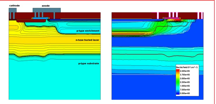
Figure 1 TCAD simulations of a BCD SPAD: net doping (left) and electric field (right) at 5 V excess bias. Simulations are performed with the Synopsys Sentaurus TCAD suite and STMicroelectronics process calibration data.
2. DEVICE STRUCTURE
Figure 1 shows the simulated cross section of our BCD SPAD. The SPAD junction is fully enclosed in a double-well pocket, formed by a dedicated n-type buried layer, for vertical isolation from the p-type substrate, and a standard n-type well, for lateral isolation. A custom retrograde Boron implant, referred in the following as enrichment, defines the SPAD active area.
With such a geometry, photons are primarily absorbed in the p-type side of the depletion layer. Therefore, avalanches are primarily initiated by minority electrons moving toward the buried multiplication region. Owing to the higher avalanche triggering probability of electrons compared to holes [5], the buried avalanche multiplication region leads to higher sensitivity compared to a typical p+/n-well SPAD junction [6].
At 25 °C the breakdown voltage of the SPAD junction is 26.2 V. Through the custom tailoring of the enrichment doping, we engineered the electric field distribution to suppress noise contributions from tunneling and field-enhanced carrier generation mechanisms within the space charge region, thus enabling operation at higher excess bias voltages than conventional CMOS SPADs.
3. DETECTOR CHARACTERIZATION
3.1 Photon detection efficiency
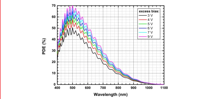
The photon detection efficiency (PDE) over the 400 nm - 1100 nm wavelength range is presented in Figure 2. The device was kept at room temperature and at excess bias ranging from 3 to 9 V. The attained PDE peak is 50%, 60% and 70% at 500 nm, when the device is biased at 3 V, 5 V and 9 V excess bias, respectively. Furthermore, the device achieves >25%
Please verify that (1) all pages are present, (2) all figures are correct, (3) all fonts and special characters are correct, and (4) all text and figures fit within the red margin lines shown on this review document. Complete formatting information is available at http://SPIE.org/manuscripts
Return to the Manage Active Submissions page at http://spie.org/submissions/tasks.aspx and approve or disapprove this submission. Your manuscript will not be published without this approval. Please contact [email protected] with any questions or concerns.
at the two extremes of the visible spectrum (i.e. at both 400 nm and 700 nm) when biased at 6 V excess bias. At the same excess bias, the PDE is still 13% at 800 nm, 8% at 850 nm and still 4.5% at 900 nm.
400 500 600 700 800 900 1000 1100 0 10 20 30 40 50 60 70 PD E (% ) Wavelength (nm) excess bias: 3 V 4 V 5 V 6 V 7 V 9 V
Figure 2 PDE vs. wavelength (at 5 nm steps) of 30 μm-diameter BCD SPAD devices operated at 3 to 9 V excess bias.
The 5 nm wavelength resolution of the spectrally resolved PDE measurements permits to finely reconstruct the interference ringing due to multiple light reflections in the back-end-of-line dielectric stack.
Figure 3 Sensitivity map of a 30 µm-diameter SPAD operated at 5 V excess bias, as measured by scanning a 850 nm laser spot (~5 nm spot size) at 1 µm steps across the SPAD.
Please verify that (1) all pages are present, (2) all figures are correct, (3) all fonts and special characters are correct, and (4) all text and figures fit within the red margin lines shown on this review document. Complete formatting information is available at http://SPIE.org/manuscripts
Return to the Manage Active Submissions page at http://spie.org/submissions/tasks.aspx and approve or disapprove this submission. Your manuscript will not be published without this approval. Please contact [email protected] with any questions or concerns.
In order to assess the PDE uniformity across the SPAD active area, we acquired the sensitivity map shown in Figure 3. At 5 V excess bias, the normalized PDE is uniform over the active area with less than 1% standard deviation, while outside its edges it drops from 0.9 to 0.1 over a length of just 3 µm. Note that no premature edge breakdown is visible. Uniformity further improves at higher excess bias, owing to the saturation of the avalanche triggering probability.
2 3 4 5 6 7 8 9 10 6 8 10 12 14 16 18 Excess bias (v) PD E @ 8 00 n m (% ) 60 80 100 120 140 160 180 DCR @ 30 0 K (cps)
Figure 4 PDE at 800 nm and DCR of a 30 µm-diameter BCD SPAD measured at 300 K as a function of excess bias.
3.2 Dark count rate
Figure 4 shows the dark count rate (DCR) as a function of the excess bias voltage of a 30 µm-diameter BCD SPAD at 300 K. The excess bias can be increased up to 9 V with little impact on DCR. Comparing the excess bias dependence of DCR and PDE in Figure 4, we can state that both curves increase and saturate in the same fashion, owing to the increase and saturation of the avalanche triggering probability. This demonstrates that field-assisted carrier generation mechanisms are negligible at 300 K and above. Conversely, most CMOS SPADs reported in the literature exhibit an exponential dependence of DCR on excess bias.
Please verify that (1) all pages are present, (2) all figures are correct, (3) all fonts and special characters are correct, and (4) all text and figures fit within the red margin lines shown on this review document. Complete formatting information is available at http://SPIE.org/manuscripts
Return to the Manage Active Submissions page at http://spie.org/submissions/tasks.aspx and approve or disapprove this submission. Your manuscript will not be published without this approval. Please contact [email protected] with any questions or concerns.
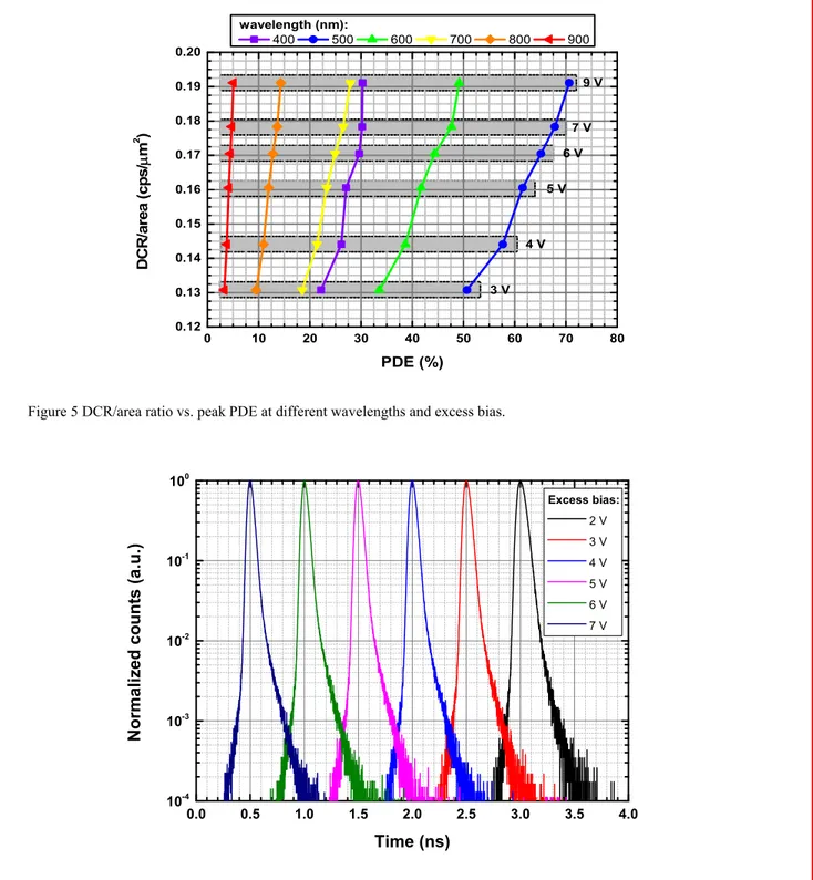
0 10 20 30 40 50 60 70 80 0.12 0.13 0.14 0.15 0.16 0.17 0.18 0.19 0.20 3 V 4 V 5 V 6 V 7 V DC R/ ar e a ( c p s/ μm 2 ) PDE (%) wavelength (nm): 400 500 600 700 800 900 9 V
Figure 5 DCR/area ratio vs. peak PDE at different wavelengths and excess bias.
0.0 0.5 1.0 1.5 2.0 2.5 3.0 3.5 4.0 10-4 10-3 10-2 10-1 100 Excess bias: 2 V 3 V 4 V 5 V 6 V 7 V Normaliz ed co unt s (a.u. ) Time (ns)
Figure 6 Photon timing response at 850 nm of a 30 µm-diameter SPAD operated at different excess bias.
From a user point of view, it is often useful to compare SPADs in a plot with DCR/area ratio vs. PDE [7], as shown in
Please verify that (1) all pages are present, (2) all figures are correct, (3) all fonts and special characters are correct, and (4) all text and figures fit within the red margin lines shown on this review document. Complete formatting information is available at http://SPIE.org/manuscripts
Return to the Manage Active Submissions page at http://spie.org/submissions/tasks.aspx and approve or disapprove this submission. Your manuscript will not be published without this approval. Please contact [email protected] with any questions or concerns.
The experimental characterizations we performed on 1024 devices from a 32x32 BCD SPAD array [8] show that the DCR reported in this paper is representative of more than 80% of the population. If we define as ‘hot’ those SPADs with a DCR higher than 10 times the average value of the best ones (i.e. those with lower DCR), the yield is higher than 90%. Note that the yield strongly depends on the SPAD active area [9] and that devices currently under investigation (square pixels with chamfered corners, 32 µm side-length, ~1,000 µm2 active area) are quite big compared to most CMOS
SPADs reported in the literature, usually smaller than 10 µm diameter. 3.3 Timing resolution
Figure 6 shows, on a log scale and after amplitude normalization, the SPAD timing response to the pulse of a gain-switching laser at 850 nm, which uniformly illuminates the entire SPAD area, acquired by a standard TCSPC setup. The measured photon-timing jitter, i.e. the full-width at half maximum (FWHM) of the photon arrival time distribution, is 41 ps, 32 ps and 28 ps at 3, 5, 7 V excess bias, respectively. The ‘diffusion tail’, which is due to minority carriers photogenerated in the quasi neutral buried layer and diffusing toward the space charge region, is almost purely exponential with a lifetime of just 50 ps, never reported so far.
Such extremely sharp timing response leads to less than 250 ps FW1/100M (full width at 1/100 from the peak), and shorter than 1 ns even down four decades from the peak (FW1/10,000M), thus being attractive to applications requiring extremely demanding timing resolution in fast optical signals with wide dynamic range.
4. CONCLUSIONS
We have reported the design criteria and experimental characterization of the first SPADs ever fabricated in a BCD technology. The achieved state-of-the-art performance enables applications requiring single-photon detection of extremely fast and sharp visible and NIR optical signals, with broad sensitivity and counting dynamics. For example, to detect background targets just behind strongly reflecting foreground objects in 3D time-of-flight LIDAR systems (e.g. a second opaque object with a factor 10,000 in reflectivity just 500 ps, i.e. 7.5 cm, beyond a first highly reflecting object, which could conceal it).
REFERENCES
[1] Bronzi, D., Zou, Y., Villa, F., Tisa, S., Tosi, A., Zappa, F., “Automotive Three-Dimensional Vision Through a Single-Photon Counting SPAD Camera,” IEEE Trans. on Intelligent Transportation Systems, vol. 17, no. 3, 782-785 (2016).
[2] Pellegrini, S., Rae, B., “Fully industrialised single photon avalanche diodes,” Proc. SPIE 10212, Advanced Photon Counting Techniques XI, 102120D (2017).
[3] Sanzaro, M., Gattari, P., Villa, F., Croce, G., Zappa, F., “Single-Photon Avalanche Diodes in a 0.16 μm BCD Technology With Sharp Timing Response and Red-Enhanced Sensitivity,” IEEE J. Sel. Topics Quantum Electron., vol. 24, no. 2, 1-9 (2018).
[4] Roggero, R., Croce, G., Gattari, P., Castellana, E., Molfese, A., Marchesi, G., Atzeni, L., Buran, C., Paleari, A., Ballarin, G., Manzini, S., Alagi, F., Pizzo, G., "BCD8sP: An advanced 0.16 μm technology platform with state of the art power devices," 2013 25th International Symposium on Power Semiconductor Devices & IC's (ISPSD), Kanazawa, 361-364 (2013).
[5] Oldham, W. O., Samuelson, R. R., and Antognetti, P., “Triggering phenomena in avalanche diodes,” IEEE Trans. Electron Devices, vol. 19, no. 6, 1056–1060 (1972).
Please verify that (1) all pages are present, (2) all figures are correct, (3) all fonts and special characters are correct, and (4) all text and figures fit within the red margin lines shown on this review document. Complete formatting information is available at http://SPIE.org/manuscripts
Return to the Manage Active Submissions page at http://spie.org/submissions/tasks.aspx and approve or disapprove this submission. Your manuscript will not be published without this approval. Please contact [email protected] with any questions or concerns.
[6] Gulinatti, A., Rech, I., Assanelli, M., Ghioni, M., Cova, S., “A physically based model for evaluating the photon detection efficiency and the temporal response of SPAD detectors,” J. Mod. Opt., vol. 58, no. 3–4, 210–224 (2011).
[7] Bronzi, D., Villa, F., Tisa, S., Tosi, A., Zappa, F., “SPAD Figures of Merit for Counting, Photon-Timing, and Imaging Applications: A Review,” IEEE Sens. J., vol. 16, no. 1, 3–12 (2016).
[8] Portaluppi, D., Conca, E., Villa, F., “32×32 CMOS SPAD Imager for Gated Imaging, Photon Timing, and Photon Coincidence,” IEEE J. Sel. Topics Quantum Electron., vol. 24, no. 2, 1-6 (2018).
[9] Villa, F., Bronzi, D., Zou, Y., Scarcella, C., Boso, G., Tisa, S., Tosi, A., Zappa, F., Durini, D., Weyers, S., Paschen, U., Brockherde, W., “CMOS SPADs with up to 500 μm diameter and 55% detection efficiency at 420 nm,” J. Mod. Opt., vol. 61, no. 2, 102–115 (2014).
Please verify that (1) all pages are present, (2) all figures are correct, (3) all fonts and special characters are correct, and (4) all text and figures fit within the red margin lines shown on this review document. Complete formatting information is available at http://SPIE.org/manuscripts
Return to the Manage Active Submissions page at http://spie.org/submissions/tasks.aspx and approve or disapprove this submission. Your manuscript will not be published without this approval. Please contact [email protected] with any questions or concerns.