UNIVERSITÀ DEGLI STUDI DI ROMA
"TOR VERGATA"
FACOLTA' DI SCIENZE MATEMATICHE, FISICHE E NATURALI
DOTTORATO DI RICERCA IN
FISICA
XXI CICLO
2005-2008Carbon Nanotubes for Solar Energy Conversion
Claudia Scilletta
A.A. 2008/2009
Docenti Guida: Prof. M. De Crescenzi, Dr. P. Castrucci, and Dr. E. Cappelli
Coordinatore: Prof. P. Picozza
To my love and to my wonderful family
Index
Introduction 1
1 Chapter 1: Solar Energy Conversion Materials: State of the Art 5 1.1. The reasons for the research on energy sources alternative to
fossil fuels 6
1.2. Principles of the most common solar to electricity energy
conversion mechanism 9
1.2.1. The solar spectrum 9 1.2.2. PV solar cells: principles and state of the art 10 1.2.3. Photo-electrochemical solar cells: principles and
state of the art 14 1.3. Carbon Nanotubes (CNTs) as building blocks for new solar
energy conversion devices 17
References 25
2 Chapter 2: Carbon Nanotubes: Structure and Properties 29 2.1. Historical excursus 30 2.2. The geometrical structure 33 2.3. Physical Properties of CNTs 36 2.3.1. Electronic properties 36
2.3.1.1.Correletion between structure and electronic properties:
the bidimensional graphene 36 2.3.1.2. Correletion between structure and electronic properties:
the dispersion equation 38 2.3.2. Optical properties 42 2.3.3. Relevant Experimental Results 43 2.4. What about MWNT properties 47
References 51
3 Chapter 3: Synthesis of Carbon Nanotubes 55
3.1. Synthesis methods 56
3.1.3 CVD 60 3.2. Growth of MWNT by CVD 62 3.3. Experimental Set-up & Synthesis 66
3.3.1. Deposition of catalyst 68 3.3.2. CNTs growth process 70 3.3.3. Morphology and structure: SEM characterization 71 3.3.4. Morphology and structure: TEM characterization 75 3.4. Decoration of MWCNTs 83 3.5. Deposition on patterned substrate 87
References 92
4 Chapter 4: Photocurrent generation in MWCNTs 95
4.1. Introduction 96
4.2. Photoelectrochemical MWCNT Properties 96
4.2.1. Experimental 96
4.2.2 MWCNTs photochemical current generation mechanism 99 4.2.3 Effect of decoration of MWCNTs with metal nanoparticles 102 4.3 Photoconductive Properties of MWCNTs based solid state devices 107
4.3.1 Experimental 107
4.3.2 Solid state MWCNTs device photocurrent generation
mechanism 113
4.3.3 Theoretical calculation and experimental results
interpretation 119 4.3.4 Effect of decoration of MWCNTs with metal nanoparticles
on solid-state device 122 4.4 MWCNTs based PV solar cell 124
References 126
Conclusions 129
APPENDIX A - Scanning Tunnelling Microscopy 133 APPENDIX B - Scanning Electron Microscopy 137 APPENDIX C - Electron Energy Loss Spectroscopy 145
Acknowledgments 149
Introduction
The exponential energy demand in the world is exhausting the available fossil fuel supply. Moreover, the energy production system based on fossil fuels has serious drawbacks in environment impact. To meet the increasing energy demand in the near future, humankind will be forced to seek environment-compatible clean alternative energy resources. Among the alternatives, solar energy stands is the most attractive, due to largest availability (120,000 TW per year), but, until now, the energy produced from solar radiation supplies a little fraction of the present energy needs. Regarding the electricity production, that produced by solar to electricity conversion is only the 0.015% of the total electricity demand. This is due to the high production cost and to the not optimized conversion efficiency. A great part of the research activity in this field is consequently devoted to increase the conversion efficiency, lowering at the same time the production cost.
It has been demonstrated that nanotechnology and nanomaterials could offer valid solutions to improve the conversion efficiency exploiting effects induced by mesoscopic scales. In this research field, the research on carbon nanotubes CNTs as building blocks for solar energy conversion devices is developing. The CNTs are composed by one or more graphene layers rolled up into cylindrical shape. Their unique optical and electronic properties, high electrochemical stability, large surface area, and cylindrical morphology able to provide reactive edges to chemical functionalization and surface modification, make them suitable for assembling innovative nanostructures for energy conversion devices.
The research activity of the group of Pr. M. De Crescenzi at Department of Physics of University of Rome “Tor Vergata” is addressed towards this direction.
The work presented in this thesis has been devoted to investigate the physical mechanisms underlying the photoresponse of MWCNTs when exploited in electrochemical cells and solid-state devices. A large part of the activity has consisted of the development of suitable strategies for the controlled growth of MWCNTs.
This thesis is structured as follows.
In Chapter 1, the state of the art of the research on solar energy conversion materials and devices are presented. In Paragraph 1.2, the principles of the most
common solar to electricity energy conversion devices, the photovoltaic cells and the photo-electrochemical cells, are described. The recent developments are as well presented. Then, in Paragraph 1.3, the recent results in employing CNTs as building blocks for new solar energy conversion devices are shown.
In Chapter 2, the structure and properties of CNTs are reported. After a brief historical excursus in Paragraph 2.1, the geometrical structure is described in Paragraph 2.2. In Paragraph 2.3, a large dissemination about theoretical predictions and experimental tools, useful to investigate the electronic nature of carbon nanotubes, is performed starting from the electronic structure of a single layer of graphene. In Paragraph 2.4 the theoretical predictions and experiments on MWCNTs electronic are shown. Despite the close similarity of MWCNTs to graphite, their density of states (DOS) show singularities similarly to the SWNTs DOS.
The experimental growth and characterization of MWCNTs is presented in Chapter 3. First, the most common techniques of deposition are described besides the growth model for nanotubes synthesised by Chemical Vapour Deposition (CVD). In Paragraph 3.3 the experimental set-up and synthesis process are described with techniques able to examine the morphology and the structure of MWCNTs product. It is shown also how, by these characterization techniques, it is possible to set the growth parameters in order to have a controlled growth of MWCNTs. Finally, in Paragraphs 3.4 and 3.5, the results on metal nanoparticles decoration of nanotubes and selective growth on patterned substrate are shown.
In the last Chapter 4, the different experiments on photocurrent generation from MWCNTs based devices are described and the relative results demonstrated. In Paragraph 4.2, photoelectrochemical MWCNT properties are studied. The interpretation of the basic mechanism for the e-h pair production is given, related to the presence of singularities in their DOS and obtained by analysing their electron energy loss spectrum (EELS). The influence of metal nanoparticles decoration is shown as well as the comparison of the photocurrent yield as a function of the radiation incident wavelength. A general model for the steady-state current generation from bare and functionalised MWCNTs is proposed. In Paragraph 4.3, solid-state
MWCNTs samples are able to produce current under illumination. An interpretation is given on the basis of theoretical calculations of DOS for a specific four-wall carbon nanotube (4WCNT). From these calculations, also the absorbance of our device is simulated. The theoretical calculations and simulations are in agreement with the experimental results (EELS spectrum and the incident photon to generated charges ratio spectrum). Also in this case a general model for the steady-state photocurrent generation is proposed. Finally, the first attempt to realize a PV cell with our MWCNTs is shown in Paragraph 4.4, comparing its performance with those of an actual silicon cell.
This work has been performed in close collaboration with the group DiaC3 directed by Dr. E. Cappelli of CNR ISC (Institute of Complex Systems). It has been partially supported financially from the Italian Foreign Affairs Ministry through Promotion and Cultural Cooperation Management, from Health Ministry and ISPESL through the strategic project entitled: “Innovative Methodologies for Risk Evaluation
Derived from Job Exposition to Nano-materials”, and from the PRIN 2005 project
“Carbon nanotubes based electronic and optoelectronic devices”, funded by the Ministry of Education, University and Research.
Chapter 1
Solar Energy Conversion Materials:
State of the Art
In this Chapter the reasons supporting the research on energy sources alternative to fossil fuels are shortly described. The attention is focused on the renewable energy and in particular on the solar energy converted into electricity. The principles of photovoltaic (PV) effect and a description of the first generation photovoltaic cell based on Si technology are summarized. The most promising development and realization of conversion devices alternative to the silicon PV cell, such as semiconductor multi-junction cells or quantum dot materials, to enhance the cost-effective conversion efficiency are reported.
Then the operative principles of photo-electrochemical cells are introduced as well as a description of the promising dye synthesized solar cells.
Finally the state of the art in the use of carbon nanotubes (CNTs) as building blocks to assembly new solar energy conversion device are described. The parallel development of photo-electrochemical cells based on single wall nanotubes (SWNTs) and the study of the properties suitable to realize solid-state conversion device are presented.
1.1 The reasons for the research on energy sources
alternative to fossil fuels
Abundant availability of clean energy is one of the greatest challenges facing the world in the 21st century. The dependence on oil and electricity has made energy a vital factor of our everyday needs. In the 20th century, the population quadrupled and our energy demand went up 16 times. The exponential energy demand is exhausting the available fossil fuel supply [1]. About 13 TeraWatts (TW) of energy is currently needed to 6.5 billion people worldwide.
Emergence of more than a billion new consumers from developing countries with a newly acquired spending capacity is increasing global CO2 emission at an alarming
rate [2]. The consumer growth in the emerging countries undermines the demand for additional energy resources and the overall impact on the environment. According to Hubbert [3], the exponential growth experienced in the last century is a transient
phenomenon, and the fossil fuel production will follow the trend of a bell shaped
curve Fig. 1 (successively modified by Campbell [4, 5] and Deffeyes [6], Fig.2).
Fig. 2. Oil and gas liquids 2004 scenario from 1930 to present day and forecast (ASPO, 2004). In the legend Heavy, Deepwater, Polar and NGL are unconventional petroleum (http://www.peakoil.net).
According to this prediction, the peak production will be attained within the next decade. Coal and natural gases are likely to supplement the energy needs but this fossil fuel production will follow the Hubbert’s peak before the end of this century. Diversification of energy supply as well as political and social compromise for conservation will become inevitable if we need to maintain a healthy global economic growth [1, 7-8].
Another important drawback in increasing the energy production system based on fossil fuels is its impact on the environment. Global warming from the fossil fuel greenhouse gases, which contribute to the climate changes, is becoming a major concern [9]. The United Nations Framework Convention on Climate Change calls for “stabilization of greenhouse-gas concentrations in the atmosphere at a level that
would prevent dangerous anthropogenic interference with the climate system 10 TW of carbon-emission-free power needs to be produced by the year 2050, almost equivalent to the power provided by all of today’s energy sources combined” [10].
In order to meet the increasing energy demand in the near future, humankind will be forced to seek environment-compatible clean alternative energy resources [8, 10]. Three major options are actually available: carbon neutral energy (fossil fuel in conjunction with carbon sequestration), nuclear power, and renewable energy. If we have to produce 10 TW energy using fossil fuels without affecting the environment, we need to find secure storage for 25 billion metric tons of CO2 produced annually. If
of a new 1 GW-electric nuclear fission plant everyday for the next 50 years somewhere on the planet. Renewable energy can be tapped from the available resources: hydroelectric resource (0.5 TW), from tides & ocean currents (2 TW), geothermal integrated over all of the land area (12 TW), globally extractable wind power (2-4 TW), and solar energy striking the Earth (120,000 TW). Among these options, solar energy stands out as the most viable choice to meet the needed energy demand.
Sunlight is today converted into electricity by exciting charge carriers in a solar cell. Solar photons can yield chemical fuel via natural photosynthesis in green plants or artificial photosynthesis in human-engineered systems. Concentrated or un-concentrated sunlight can produce heat for direct use, or further conversion to electricity (Fig. 3).
Fig. 3. Types of possible sunlight exploitations [11].
Despite this huge resource, the energy produced from solar radiation supplies a little fraction of the energy needs. For example solar electricity supply just 0.015% of the total electricity demand. This is due to cost (the solar electricity costs between 5 and 10 times the electricity from the fossil fuel) and conversion capacity, namely conversion efficiency. The cost and capacity limitations on solar energy exploitation are most effectively addressed by a single research objective: cost-effectively raising conversion efficiency. The best commercial solar cells based on single-crystal silicon are about 18% efficient. Laboratory solar cells based on cheap dye sensitization of oxide semiconductors are typically less than 10% efficient, and those based on even cheaper organic materials are 2-5% efficient [11].
Those efficiencies are far below their theoretical limits. The capacity to design nanostructured semiconductors, organic-inorganic hybrid assemblies, and molecular assemblies opens up innovative ways to create a new generation of solar energy
conversion devices that can deliver high efficiency devices at economically viable costs.
During the past decade, nanomaterials have emerged as the new building blocks to construct light energy harvesting assemblies. Organic and inorganic hybrid structures, that exhibit improved selectivity and efficiency toward catalytic processes, have been prepared. Size dependent properties such as size quantization effects in semiconductor nanoparticles and quantized charging effects in metal nanoparticles provide the basis for developing new and effective systems [12-15]. These nanostructures provide innovative strategies for designing next generation energy conversion devices [16-21]. Strategies to integrate ordered assemblies of semiconductor and metal nanoparticles, organic-inorganic hybrid systems, and carbon nanostructures in the energy conversion schemes are discussed in the following sections.
1.2 Principles of the most common solar to electricity
energy conversion mechanism.
1.2.1. The solar spectrum.
Solar radiation is the electromagnetic energy emitted by fusion processes of the hydrogen contained into the sun into Helium atoms. Its spectrum is very close to that of a black-body at temperature of about 5900 K.
The sun irradiates through the space a light characterized by an electromagnetic spectrum ranging from 0,2 μm up to more than 5 μm, i.e. from Ultraviolet (UV) to Infrared (IR) radiation through the visible light. The solar radiation spectrum outside and inside the Earth’s atmosphere, with the characteristic absorption bands of gas molecules composing it, is reported in Fig. 4.
Fig. 4. Solar irradiation curves outside and inside the Earth's atmosphere. The absorption bands are labeled with the names of the molecules which cause radiation absorption.
1.2.2 PV solar cells: principles and state of the art.
The Photovoltaic effect is known since 1839 thanks to the work of the French physicist A.E. Becquerel (1820-1891), who presented to the Science Academy of Paris his “Mémoire sur les effets électriques produits sous l’influence des rayons
solaires”. The discovery accidentally occurred during experiments on an
electrochemical cell in which two platinum electrodes were immersed. For a long time it remained a scientific phenomenon with few device applications. In 1870 the PV effect was studied by H. Hertz on solid-state selenium and, in 1876, by Smith, Adam, and Day which prepared such devices converting solar energy into electricity with an efficiency of 1-2%. The development of PV effect as an energy source was hindered by the low yield of the used materials. Only in 1954 Person, Fuller, and Chaplin [22] obtained the first silicon-based PV module at the Bell Laboratory. Owing to the introduction of silicon as the standard industrial semiconductor material in the late 1950s, silicon PV diodes became available.
A PV solar cell is basically a semiconductor p-n diode. The semiconductor material absorbs the incoming photons and converts them into electron-hole pairs.
The fundamental parameter is the semiconductor bandgap energy EG (∼1.1 eV for Si). In an ideal case, no photons with an energy hν < EG will contribute to photogeneration, whereas all photons with an energy hν > EG will each produce an electron-hole pair. The excess energy (hν - EG) is very rapidly lost because of thermalization (Fig. 5). The maximum limit for the photogenerated electric current density Jph is therefore given by the flux of photons with an energy hν > EG. Thus Jph
decreases with an increasing of EG. At the same time, the net energy transferred to each electron-hole pair increases, as it is equal to EG. There exists an “optimum” value for EG for which a maximum of energy can be transferred from the incident sunlight to the totality of photogenerated electron-hole pairs. At this bandgap, roughly half of the incident solar energy is transferred.
Fig. 5. Schematic picture showing the interaction of a p-n junction with photon of different energy. Photons with energy smaller than the semiconductor energy bandgap, hν < EG, are not absorbed, while photons with energy exceeding EG are absorbed producing a charge pair. The energy excess (hν - EG) is lost by thermalization. The charge carriers are separated and
collected by the photovoltage.
The second step of the energy conversion process, the photogenerated electron-hole pairs are separated, with electrons drifting to one electrode and electron-holes drifting to the other electrode, because of the internal electric field created by the p-n junction structure of the solar cell. The dark (non illuminated) and the photogenerated characteristics of the photodiode can be linearly superimposed. The resulting solar cell equivalent circuit is shown in Fig. 6A and the relative I-V characteristics are shown in Fig. 6B. The characteristic parameters of solar cells are: short circuit Isc, open circuit Voc, and fill factor FF.
The fill factor is essentially a measure of quality of the solar cell. It is calculated by comparing the maximum power to the theoretical power that would be output at
parameter that takes into account the form of the I-V curve under irradiation, being the ratio between the maximum area of the inscribable rectangle, Pmax, and the rectangle identified by Isc, and Voc :
(1) max sc oc P FF I V = ⋅ ,
the maximum limit for Isc is given by the photogenerated current density Iph.
Fig. 6. Equivalent circuit (A) and the I-V characteristics (B) of a p-n PV solar cell.
To test the performance of the PV cell the efficiency η is evaluated. The efficiency is defined as:
(2) max cell P E A η= × ,
where E is the irradiance of radiation (W/m2) and Acell is the illuminated area of the cell. It is worth to notice that η has to be distinguished from the quantum efficiency,
QE at fixed photon energy (hν) (or equivalent the incident photon conversion efficiency, IPCE) that is defined as the ratio between the number of generated
charges, Ne-h , and the number of incident photons Nph:
(3) ( ) ( ) ( ) e h ph N QE h IPCE h N h υ υ υ − = = .
QE takes into account the charge photogeneration capability of materials,
The loss of photon energy into heat is one of the reasons why the calculated maximum efficiency of conventional solar cells is limited to about 32%. Other reasons are represented by the reflection of photon onto the cell surface, the electron-hole pair recombination before to be collected by the electrodes, the presence of shunt resistances at the semiconductor/metal junctions.
The overall conversion efficiency depends on each of the described mechanisms. Monocrystalline Si cells reach an efficiency of 25% at a laboratory level, while for commercial modules the efficiency is about 15%.
Recently, different devices have been designed to increase the overall efficiency. Stacked cells composed by semiconductor of different bandgap allow to absorb a greater fraction of the solar spectrum enhancing the overall conversion efficiency. These are referred to as "multijunction" cells (also called "cascade" or "tandem" cells). Much of today's research in multijunction cells focuses on III-V semiconductors as cell components. Such cells have reached efficiencies of around 35% under concentrated sunlight, but their production costs are remarkably high.
The most dramatic and surprising potential increase in efficiency comes from nanotechnology application. For example, in quantum-dots, carrier multiplication [23, 24] allows the generation of multiple electron-hole pairs for a single incident photon. Theoretical efficiencies exceeding 60% would, in principle, be achievable. Then, absorbers having a highly quantized band structure, such as quantum wells and quantum dots, can theoretically produce the desired effects (Fig. 7).
Fig. 7. Possible methods of circumventing the 31% efficiency limit for thermalized carriers in a single–band gap absorption threshold solar quantum conversion system. (A) Intermediate-band solar cell; (B) quantum-well solar cell [25].
In fact, recent observations on PbSe quantum dots have demonstrated the production, with high quantum yield, of multiple excitons from a single absorbed photon, thereby establishing an existence proof for the process of interest [23]. At present, however, there is no method for efficiently extracting the photogenerated carriers from the quantum dot structure to produce electricity in an external circuit. Materials with “mini-bands” or with “intermediate bands” also offer the possibility for ultrahigh energy conversion efficiency [23]. According to this approach, different incident photon energies would promote absorption from different isolated energy levels and therefore allow for the production of different voltages (Fig.7). The phenomenon has been described theoretically but has yet to be demonstrated in a practical implementation. In addition, these materials are currently extremely costly, and methods of retaining the high performance with scalable, inexpensive manufacturing methods should also be required.
1.2.3 Photo-electrochemical solar cells: principles and state
of the art
Photo-electrochemical (PEC) systems represent the best-known wet chemical method to converting sunlight into electrical energy or chemical fuels. PEC cells developed during the mid-1970s and 1980s for capture and conversion of solar energy into electricity and fuels worked with a semiconductor electrode in contact with an electrolyte solution (Memming 2001; Bard et al. 2002; Nozik and Memming 1996; Nozik 1978; Grätzel 2001).
In a first configuration (called an electrochemical photovoltaic (EPV) cell), a semiconductor is in contact with an electrically conducting liquid, the electrolyte, that is able to provide a redox reaction that can readily transfer electrons to an electrode and can accept electrons from the other electrode (Fig. 8). The semiconductor forms a junction with the liquid by simple immersion and develops an electric field at its surface. The semiconductor can be n-type or p-type. Upon illumination of the semiconductor, the photogenerated electrons and holes can separate because of the surface electric field. For n-type semiconductors, the holes move to the surface and are captured by a redox couple; the electrons move to the back side of the semiconductor, where they leave the cell via an electrical contact, deliver electrical
electrode. Here, they are scavenged by the redox species that initially had captured the hole at the semiconductor surface; this process returns the redox species to their original chemical condition. Thus the redox couple accepts holes at one electrode and accepts electrons at the other electrode, resulting in charge neutralization and no net change in the redox species. The electrolyte and redox couple just serves to complete the electrical circuit and to produce the electric field required for charge separation.
Fig. 8. Schematic picture of the basic mechanisms for photocurrent generation in electrochemical photovoltaic cells (EPV).
Hence, in a typical photochemical solar cell, a semiconducting film serves as a photoactive electrode that, under excitation of visible light, generates electron-hole pairs. As one of the charge carriers (e.g. the electron) is driven to the counter electrode, the other charge carrier (e.g. the hole) is scavenged by a redox reaction.
New architecture of inorganic nano-crystalline semiconductors and molecular structures [26] are being developed to enhance the performance of a photoelectric solar cell such as overall conversion efficiency and the lifetime of the active electrode besides a reduction of the costs.
Dye-sensitized solar cells (DSSC), invented by M. Graetzel and collaborators in 1991, introduce a new concept solar conversion device and represent a feasible alternative to p-n junction photovoltaic devices [27]. In contrast to the conventional semiconductor systems, where the expensive semiconductor assumes both the task of photon capture and charge transport, these two functions are separated in the DSSC. A hybrid system, formed by a chemical dye and the inexpensive wide-bandgap semiconductor TiO2 nanoparticles, replaces the bulk semiconductor. Light is absorbed
by the sensitizer, while the charge separation takes place at the interface via photo-induced electron injection from the dye into the conduction band of the solid. Charge
carriers are then transported from the conduction band of the semiconductor to the charge collector. The holes left in the dye molecule recombines with the electrons carried to it through an electrolyte from the counter electrode by an anion. The use of sensitizers, having a broad absorption band, in conjunction with optically–transparent electrically-conducting oxide films of nanocrystalline structure, permits to harvest a large fraction of sunlight. The conversion of incident photons into electric current is achieved over a large spectrum ranging from the UV to the near IR region. Overall solar radiation to electric current conversion efficiencies of 10.6% have been reached.
In Fig. 9 the operation principles and energy level scheme of dye-sensitized nanocrystalline solar cell are drawn [28]. Photoexcitation of the sensitizer (S) is followed by electron injection into the conduction band of a semiconductor oxide film. The dye molecule is regenerated by the redox system, which itself is regenerated at the counter electrode by electrons passing through the load. The open-circuit voltage of the solar cell corresponds to the difference between the redox potential of the mediator and the Fermi level of the nanocrystalline film indicated with a dashed line.
Fig. 9. Principle of operation and energy level scheme of the dye-sensitized nanocrystalline solar cell. Photoexcitation of the sensitizer (S) is followed by electron injection into the conduction band of an oxide semiconductor film. The dye molecule is regenerated by the redox system, which itself is regenerated at the counter-electrode by electrons passed through the load. Potentials are referred to the normal hydrogen electrode (NHE). The open circuit voltage of the solar cell corresponds to the difference between the redox potential of the mediator and the Fermi level of the nanocrystalline film indicated with a dashed line. The energy levels drawn for the sensitizer and the redox mediator match the redox potentials of the doubly deprotonated N3 sensitizer ground state and the iodide/triiodide couple.
1.3 Carbon Nanotubes (CNTs) as building blocks for
new solar energy conversion devices
The unique optical and electronic properties, high electrochemical stability, large surface area, and cylindrical morphology providing reactive edges to chemical functionalization and surface modification, have prompted many researchers to employ carbon nanostructures assemblies for energy conversion devices [29].
The simplest carbon nanotube is composed by a graphene, a single sheet of a honeycomb network of carbon atoms, rolled up seamlessly into a tubular shape [30]. The first discovered carbon nanotubes were composed of multi-tubes (multi-wall tubes, MWNT) nested in a concentric way [31]. Later, a single-wall carbon nanotube, SWNT, was discovered by Iijima himself [32]. Since the first reports, CNTs have been subject of intense interest for basic and applied research. Interest in carbon nanotubes is driven by their exceptional electronic, optical, thermal, and mechanical properties [30, 33]. In particular, depending on the way the sheet is rolled up (i.e. its chirality) the CNT may show metallic or semiconducting properties (while a graphene layer is a semi-metal). Semiconducting nanotubes are direct bandgap semiconductors with EG ≈ 0.8/D (eV), where D is the nanotube diameter in nanometers. The work
function of SWNT bundles is known to be about -4.8 eV [34].
Recently researchers have used SWNTs as building blocks for solar energy conversion devices in chemical cells. Two different approaches have to be considered for the use of carbon nanotubes in solar cells (Fig. 10): (i) direct bandgap excitation of semiconducting nanotubes; or (ii) the use of conducting tubes as low-impedance conduits to improve the transport of charge carriers from light-harvesting nanoassemblies.
Fig. 10. Schematic picture of CNT based photoelectrochemical cells. The nanotubes can be used to produce the charges (picture on the left) and to collect and transport the charges in hybrid structures (picture on the right).
(i) Semiconducting SWNTs seem to be very promising optoelectronic materials.
First semiconducting nanotubes have a direct gap. This is a desirable property for an optoelectronic material since it allows optical transitions to proceed without the intervention of phonons. Furthermore, the low dimensionality leads to a diverging density of states (Fig. 11) at the band edge, defined as van Hove singularities. That allows electronic transitions among singularity pairs, making several features emerge in the optical absorption spectrum in the visible and near IR range [35-37].
Fig. 11. DOS exhibiting the valence and the conduction band for a metallic tube, which shows electronic states at the Fermi level, and for a tube revealing semiconducting behavior due to the presence of an energy gap. The spikes shown in the DOS of the tubules are called van Hove singularities and are the result of the one-dimensional quantization, which is not present in an flat graphite single layer.
Finally, their one-dimensional confinement causes a strongly Coulombic coupling between the photogenerated electron-hole pairs, resulting in strongly bound excitons [38, 39]. The lifetime of such states is very long (τ ~ 10-9 sec) in CNTs in respect to
the lifetime of excited states in solids (τ ~ 10-16 sto 10-14). This allows the electrolyte
to separate the charges: the electrons (holes) are driven away to the collecting electrode surface and the holes (electrons) are scavenged by the redox producing a steady current.
The first experiment on a similar solar cell was performed by Kamat et al. [40]. He measured the photoresponse of a SWNTs film in a PEC cell after excitation under visible light. This photoresponse extends up to the visible-red region, in agreement with the absorption spectrum. The maximum generated photocurrent was 8 µmA/cm2 for a wavelength of 400 nm, while the maximum incident photon conversion efficiency was only 0.15%. This value was very low, but they showed for the first time the photovoltaic property that characterizes the p-type semiconducting nature of single-wall carbon nanotubes. Recently, the group directed by Prof. De Crescenzi at Tor Vergata University demonstrated that also MWCNTs are able to generate a significant photocurrent if exposed under a monochromatic radiation ranging from visible to UV radiation [41]. In this work MWCNTs show photon-to-current conversion efficiency at maximum up to 7% at 350nm, about 50 times higher than that of SWCNTs. This is very surprising owing to the fact that, for SWNT the current generation can be ascribed to the Van Hove singularities that were theoretically calculated and experimentally verified, while for MWNTs no ab-initio calculation has been yet achieved. On the contrary, current generation under light irradiation was unexpected due to the close similarity of a MWNT to the graphite structure (number of walls > 9 in [41]).
(ii) A lot of work has been made to prepare photochemical solar cells based on
new hybrid architectures that exploit carbon nanotubes, in particular single-wall, to improve the capture of photogenerated charges and their transport to the electrode surface.
SWNTs are ideal candidates as conduits for collecting and transporting charges across light-harvesting assemblies (e.g. semiconductor particles). A CdS-SWNT composite has shown unusually high efficiency, generating a photocurrent from visible light [42,43], while using SWNT as conducting scaffolds in a TiO2-based
photoelectrochemical cell can increase the conversion efficiency by a factor of 2 [44] (Fig.12).
Fig. 12. (A) Photocurrent response vs time of SWCNT/TiO2 (a) and TiO2 (b) electrodes at 0 V vs SCE, with a light intensity of 50 mW/cm2 (hν > 300 nm). (B) IPCE spectra of SWCNT/TiO2 (a, b) and TiO2 (c, d). The electrodes are at a floating applied bias (b, d) and at 0 V (a, c). Electrolyte was a N2-saturated 1M KOH solution [44].
Another successfully utilization of SWNT is represented by the realization of organic/inorganic solar cells. SWNTs have a characteristic curve-shaped surface that facilitates binding of larger organic molecules via non-covalent or hydrophobic interactions. Molecules as porphyrins have an affinity to bind non-covalently with SWNTs through π-π interactions. The interaction between porphyrins and SWNTs can be modulated to achieve a supramolecular assembly. Exploiting this property, ordered assembly of SWNT with porphyrin systems as photoactive electrode of a photoelectrical solar cell have been realized and their performance have been tested [45-47]. These systems give rise to promising solar-energy conversion efficiencies (up to 8.5% internal photoconversion efficiencies (IPCE) [46]).
Besides the research on photo-electrochemical cells, also the possibilities to exploit the nanotubes to realize solid-state devices generating current under illumination are undergoing intense research study. Initially the optoelectronic properties of nanotubes has been studied. Electrically induced polarized IR optical emission have been experimentally observed from SWNT field-effect transistor (FET) [48] giving rise to the possibility to fabricate nanotube-based optical emitters in the infrared range. At the same time photoconductivity of SWNTs [49-51] has been
observed, outlining the possibility to fabricate nanotube optical detectors over a wide IR and visible range. Freitag [49] measured the infrared laser-excited photoconductivity from a single carbon nanotube constituting the channel of a field-effect transistor (FET). In his experiment the e-h couples generated within the nanotube have been separated by an electric field applied between the metallic contacts. He ascribed the photocurrent generation to the resonant excitation of the semiconducting nanotube second exciton state with an estimated quantum efficiency of about 10%. A further step is the experiment of Mohite on the photoconductivity of a SWNTs film. In this experiment, a film of semiconducting and a film of metallic SWNTs are deposited on a glass slide which are then anchored to a copper block. Contact to the SWNTs is performed by attaching a gold wire to the film surface using silver paint. The sample is illuminated by a pulsed light tunable from 0.4 to 4.0 eV; a scheme of the device and measurement is reported in Fig. 13.
Fig. 13. Sketch illustrating the displacement photocurrent measurement technique [51].
The generated photocurrent shows resonances whose energies are in agreement with the energies of exciton states of both semiconducting and metallic nanotubes (van Hove transitions, Fig. 14). Moreover the constant value of the photocurrent sign suggest the existence of a built-in potential that aids the electron transfer from the SWNT/glass interface towards the silver contact.
Fig. 14. (a) Peaks in the photocurrent are observed at the two lowest energy semiconductor transitions (S11 and S22) and at the lowest energy metallic transition (M11). (b) The absorbance measured for the same SWNT film under the same conditions. The generated photocurrent is directly related to the semiconducting and metallic transitions in the nanotube absorbance spectrum.
The optoelectronic properties of CNTs are often related to the presence of p-n junctions arising from an applied bias [49], a modulated chemical doping, a crossed-wire geometry [52], or the presence of non-equivalent Schottky barriers at the junctions CNTs/electrodes [49,51]. Photocurrent has been calculated in nanotube p-n junctions [53] showing multiple sharp peaks, ranging from the IR to the UV, through the visible owing to the fact all the bands in the SWNT have a direct band gap, which leads to a response over a wide energy spectrum. Lee [54] tested the PV effect of individual SWNTs forming ideal p-n junction diodes realized by using electrostatic doping [55]. The scheme of such device is shown in Fig. 15.
Fig. 15. Split gate device where VG1 and VG2 are biased with opposite polarities VG1=−VG2= +10 V to form an ideal p-n junction diode along the SWNT [54].
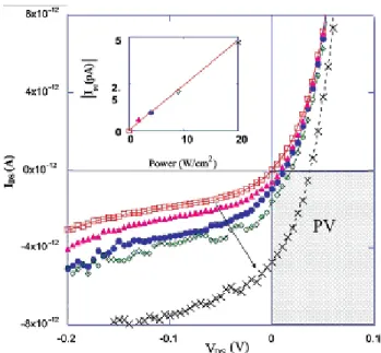
The I-V characteristics in dark conditions and under illumination of a 1.5 µm continuous laser are reported in Fig.16 as a function of the illuminated power, showing the PV behavior of the nanotube. The total efficiency η of this PV cell is estimated to be around 5% (considering the actual absorbed power).
Fig. 16. I-V characteristics under increased light intensity showing a progressive shift into the fourth quadrant (PV) where the diode generates power. The inset shows the expected linear increase in the current measured at VDS=0 (Isc) with illuminated power [54].
A further and recent step is the realization of a double-walled nanotube (DWNT) solar cell [56]. These solar cells consist of a semitransparent thin film of CNTs on a n-type crystalline silicon substrate to create high-density p-n hetero-junctions between nanotubes and Si and thus favour charge separation as well as electrons (through n-Si) and holes (through nanotubes) extraction (Fig.17). Initial tests have shown a power conversion efficiency of > 1%.
Fig. 17. Picture of the DWNT/n-Si solar cell device fabricated by Wei [56].
A question is if also MWCNTs, which have a close similarity with graphite (metallic), show photocurrent generation properties under illumination and if they can
be eventually used like materials for photovoltaic solar cell. First results have been obtained by Passacantando and coworkers on MWCNTs sheets grown on a sapphire substrate [57]. They have shown the capability of MWCNTs to generate photocurrent upon illumination with white light and monochromatic radiation in the UV–visible– near IR region.
Nonetheless many issues remain open, more in general a deep comprehension of the inner mechanisms of a steady - state current generation by MWCNTs, in photochemical cell or solid-state devices, under irradiation has to be yet carried on. This is the main aim of this thesis.
References
[1] P. B. Weisz, Phys. Today, July 2004, 47.
[2] N. Myers, J. Kent, Proc. Natl. Acad. Sci. U.S.A. 100, 4963 (2003).
[3] M. K. Hubbert, Am. J. Phys. 49, 1007 (1981).
[4] C. J Campbell, Popul. EnViron. 24, 193 (2002).
[5] C. J. Campbell, J. H. Laherrere, Sci. Am. 278, 60 (1998).
[6] K. S. Deffeyes, ‘Hubbert’s Peak: The Impending World Oil Shortage’,
Princeton University Press: Princeton, NJ, 2001.
[7] M. S. Dresselhaus, I. L. Thomas, Nature 414, 332 (2001).
[8] A. J. Ragauskas, et al.; Science 311, 484 (2006).
[9] M. E. Mann, R. S. Bradley, M. K. Hughes, Nature 392, 779 (1998).
[10] M. I. Hoffert, et al, Science 298, 298 (2002).
[11] G.W. Crabtree, N.S. Lewis, Physics Today, March 2007, 37.
[12] M. L. Steigerwald, L. E. Brus, Acc. Chem. Res. 23, 183 (1990).
[13] L. E. Brus, J. Phys. Chem. 90, 2555 (1986).
[14] H. Weller, Adv. Mater. 5, 88 (1993).
[15] L. Banyai, S. W. Koch, ‘Semiconductor quantum Dots’, World Scientific
Publishing Co.: River Edge, NJ, 1993.
[16] P. V. Kamat, J. Phys. Chem. B 106, 7729 (2002).
[17] D. Adams, et al.; J. Phys. Chem. B 107, 6668 (2003).
[18] K. George Thomas, P. V. Kamat, Acc. Chem. Res. 36, 888 (2003).
[19] A. N. Shipway, E. Katz, I. Willner, Chem. Phys. Chem. 1, 18 (2000).
[20] I. Willner, E. Kaganer, E. Joselevich, H. Durr, E. David, M. J. Gunter, M. R. Johnston, Coord. Chem. Rev. 171, 261 (1998).
[21] M. D. Ward, Chem. Soc. Rev. 26, 365-375 (1999).
[23] R.D. Schaller, M.A. Petruska, V.I. Klimov, Appl. Phys. Lett. 87, 253102 (2005).
[24] A.J. Nozik, Physica E 14, 115 (2002).
[25] Adapted from “Basic Research Needs for Solar Energy Utilization”, U.S.
Department of Energy, Washington, DC, 2005, available on the web at http://www.sc.doe.gov/bes/reports/files/SEU_rpt.pdf.
[26] M. Graetzel, Nature 414, 338 (2001).
[27] B. O’Regan, M. Graetzel, Nature 353, 737 (1991).
[28] M. Graetzel, Inorg. Chem 44, 6841 (2005).
[29] P.V. Kamat, Nanotoday 1, 20 (2006).
[30] R. Saito, G. Dresselhaus, and M. Dresselhaus, Physical Properties of Carbon Nanotubes, Imperial College Press, 1998.
[31] S. Iijima, Nature 354, 56 (1991).
[32] S. Iijima and T. Ichihasi, Nature 363, 603 (1993).
[33] P.L. McEuen, M. S. Fuhrer, and Park Hongkun, IEEE Trans. on Nanotechnology 1, 78 (2002).
[34] S. Suzuki, et al., Appl. Phys. Lett. 76, 4007 (2000).
[35] J. Chen, M. A. Hamn, H. Hu, Y. Chen, A. M. Rao, P. C. Eklund, and R. C. Haddon, Science 282, 95 (1998).
[36] H. Kataura, Y. Kumazawa, Y. Maniwa, I. Umezu, S. Suzuki, Y. Ohtsuka, and Y. Achiba, Synth. Met. 103, 2555 (1999).
[37] Z. M. Li, Z. K. Tang, H. J. Liu, N. Wang, C. T. Chan, R. Saito, S. Okada, G. D. Li, J. S. Chen, N. Nagasawa, and S. Tsuda, Phys. Rev. Lett. 87, 127401 (2001).
[38] C. L. Kane, E. J. Mele, Phys. Rev. Lett. 90, 207401 (2003).
[39] T. G. Pedersen, Phys. Rev. B 67, 073401 (2003).
[40] S. Barazzouk, S. Hotchandani, K. Vinodgopal, and P. V. Kamat, J. Phys. Chem. B 108, 17015 (2004).
[41] P. Castrucci, F. Tombolini, M. Scarselli, E. Speiser, S. Del Gobbo, W. Richter, M. De Crescenzi, M. Diociaiuti, E. Gatto, M. Venanzi, Appl. Phys Lett. 89,
253107 (2006).
[42] L. Sheeney-Haj-Ichia, et al., Angew. Chem. Int. Ed. 44, 78 (2004).
[43] I. Robel, et al., Adv. Mater. 17, 2458 (2005).
[44] A. Kongkanand, R. Martinez Dominguez, and P.V. Kamat, Nanoletters 7, 676
(2007).
[45] T. Hasobe, et al., J. Am. Chem. Soc. 127, 11884 (2005).
[46] D. M. Guldi, G. M. A. Rahman, M. Prato, N. Jux, S. Qin, and W. Ford, Angew. Chem. Int. Ed. 44, 2015 (2005).
[47] T. Hasobe, et al., J. Am. Chem. Soc. 125, 14962 (2003).
[48] A. Misewich, R. Martel, Ph. Avouris, J. C. Tsang, S. Heinze, and J. Tersoff,
Science 300, 783 (2003).
[49] M. Freitag, Y. Martin, J. A. Misewich, R. Martel, P.H. Avouris, Nanoletters 3,
1067 (2003).
[50] K. Balasubramanian, Y. Fan, M. Burghard, K. Kern, M. Friedrich, U.Wannek, and A. Mews, Appl. Phys. Lett. 84, 2400 (2004).
[51] A. Mohite, S. Chakraborty, P. Gopinath, G. U. Sumanasekera, and B. W. Alphenaara, App. Phys. Lett. 86, 061114 (2005).
[52] M.S. Fuhrer et al., Science 288, 494 (2000).
[53] D. A. Stewart, F. Leonard, Phys. Rev. Lett. 93, 107401 (2004).
[54] J.U. Lee, Appl. Phys. Lett. 87, 073101 (2005).
[55] J. U. Lee, P. P. Gipp, and C. M. Heller, Appl. Phys. Lett. 85, 145 (2004).
[56] J. Wei,Y. Jia, Q. Shu, Z. Gu, K. Wang, D. Zhuang, G. Zhang, Z. Wang, J. Luo, A. Cao, and D. Wu, Nanoletters 7, 2317 (2007).
[57] M. Passacantando, F. Bussolotti, V. Grossi, S. Santucci, A. Ambrosio, M. Ambrosio, G. Ambrosone, V. Carillo, U. Coscia, P. Maddalena, E. Perillo, and A. Raulo, Appl. Phys Let. 93, 051911 (2008).
Chapter 2
Carbon Nanotubes: Structure and
Properties
Carbon nanotubes (CNTs) are quasi-one dimensional crystals with the shape of hollow cylinders made of one or more graphite sheets; their size is typically µm in length and 1 to tens of nm in diameter. Because of many interesting properties that carbon nanotubes exhibit and their possible applications, CNTs have emerged to be one of the most intensively investigated nanostructure materials since their discovery. In this Chapter a brief historical review of carbon nanotube research is presented. Then a more detailed description of the geometrical structure and the physical properties of nanotubes are described. In particular the electronic and optical properties are focused in consideration of the main aim of this thesis, i.e. to verify and understand the mechanisms of measured photocurrent generation in multiwall carbon nanotubes both used in photoelectrochemical cells and in solid-state device.
2.1 Historical excursus
Carbon appears in several crystalline modifications, as a result of its flexible electron configuration. The carbon atom has six electrons; the 2s orbital and the 2p orbitals can form an sp2 or sp3 hybrid, respectively. The sp3 configuration gives rise to the tetrahedrally bonded structure of diamond. The sp2 orbitals lead to strong in-plane bonds of the hexagonal structure of graphite and the remaining p-like orbital to weak bonds between the planes. In 1985 Kroto et al discovered a modifications of crystalline carbon the so-called buckyballs [1]. This discovery was very important because not just a single new molecule was found but an infinite class of new molecules: the fullerenes. Each fullerene – C60, C70, C84, etc. – possessed the essential
characteristic of being a pure carbon cage, each atom bonded to three others as in graphite. Unlike graphite, every fullerene has exactly 12 pentagonal faces with a varying number of hexagonal faces. Some fullerenes, like C60, were spheroidal in
shape, and others, like C70, were oblong like a rugby ball. The most famous one of the
buckyballs is probably C60, a spherical molecule formed by 20 hexagons. Dr. R.
Smalley recognized in 1990 that, in principle, a single wall carbon nanotube, SWNT, might be a limiting case of a fullerene molecule: a tubular fullerene capped at each end, for example, by the two hemispheres of C60, connected by a straight segment of
tube, with only hexagonal units in its structure. M. Dresselhaus, upon hearing of this concept, dubbed these imagined objects “buckytubes.”
Actually carbon nanotubes had been discovered 30 years earlier, but had not been fully appreciated at that time. In the late 1950s, Roger Bacon at Union Carbide, found a strange new carbon fibre while studying carbon under conditions near its triple point. He observed straight, hollow tubes of carbon that appeared to consist in graphitic layers of carbon separated by the same spacing as the planar layers of graphite. In the 1970s and 1980s, Morinobu Endo observed these tubes again, produced through the synthesis of vapor grown carbon fibers by the decomposition of hydrocarbons at high temperatures in the presence of transition metal catalyst particles of < 10 nm diameter. Indeed, he even observed some tubes consisting in only a single layer of rolled-up graphite. [2-4].
But the discovery of nanotubes is ascribed to Sumio Iijima of the NEC Laboratory in Tsukuba (Japan) who observed multiwall nanotubes, MWNT, formed in a carbon arc discharge in 1991 [5]. Multiwall carbon nanotubes (see Fig.1) contain several
coaxial cylinders, each cylinder being a single-wall carbon nanotube, nested as Russian dolls.
Fig. 1. The observation by TEM of multi-wall coaxial nanotubes with various inner and outer diameters, di and do, and numbers of cylindrical shells N reported by Iijima in 1991: (a) N = 5, do = 67 Å, (b) N = 2, do = 55 Å and (c) N = 7, di = 23 Å, do = 65 Å [5]
Two years later Sumio Iijima and Donald Bethune and coworkers at the IBM Almaden Laboratory independently observed SWNTs [6,7]. This has allowed a great number of theoretical studies and predictions that preceded the experimental observation of single wall carbon nanotubes. On the contrary, until now very few ab-initio calculations have been performed to predict the properties of MWNT due to the very large numer of carbon atom to take in account. The most fundamental of the theoretical developments on SWNTs was the prediction that carbon nanotubes could be either semiconducting or metallic depending on their diameter and orientation of their hexagons with respect to the nanotube axis (chiral angle) [8-10]. These predictions were experimentally confirmed in 1998 [11,12].
Moreover carbon nanotubes are intriguing from a fundamental physics point of view. In contrast to many quasi-one-dimensional systems in semiconductor physics, where carriers are artificially restricted to a one-dimensional phase space by sophisticated fabrication like cleaved-edge overgrowth [13,14] or experiments in the
quantum-Hall regime [15], carbon nanotubes are natural quasi-one-dimensional systems with ideal periodic boundary conditions along the circumference. Their one-dimensional character has been manifested in many experiments like scanning-tunneling spectroscopy, where the singularities in the density of states typical for one dimension have been measured [12, 16-17]. Then, for example, they appear an ideal system for the study of Luttinger liquid behaviour [18,19]; ballistic transport at room temperature up to several µm was reported [20] and, if defects or electrical contacts act as boundaries, zero-dimensional effects such as Coulomb blockade are observed [21,22].
Of course it has been taken into account that actual CNTs have finite length, contain defects, and interact with other nanotubes or with the substrate and these factors often complicate their behaviour in respect to the theoretical predictions.
The remarkable physical properties exhibited by carbon nanotubes paved the way to many possible applications of carbon nanotubes both on the nanometer scale and in the macroscopic range that attracted great attention and expectations. In nanoelectronics, it has been demonstrated that is possible to connect nanotubes with different chiralities creating nanotube heterojunctions to be used as nanoelectronics devices [23,24] such as nanoscale p-n junctions [25], field effect transistor [26-28] and single-electron transistor [29,30]. Recently CNTs have been used for many and different applications of great technological importance: conductive wires [31-33], new optoelectronic devices [34], photosensitive transistors [35], innovative solar cells [36,37], or chemical sensors [38,39]. Prototype devices using the superior field emission properties of nanotubes [40] have been also demonstrated. These devices include x-ray tubes [41], scanning x-ray sources [42], flat panel displays [43], and lamps [44].
Single and multi-wall nanotubes have also very good elasto-mechanical properties because the two dimensional arrangement of carbon atoms in a graphene sheet allows large out-of-plane distortions, while the strength of carbon-carbon in-plane bonds keeps the graphene sheet exceptionally strong against any in-plane distortion or fracture. These structural and materials characteristics of nanotubes point towards their possible use in making next generation of extremely lightweight but highly elastic and very strong composite materials (torsional springs [45,46] or as single vibrating strings for ultrasmall force sensing).
A major difficulty for the applications is the variety of nanotube structures that are produced simultaneously; in particular a growth method which determines whether the tubes will be metallic or semiconducting is still not available. Instead, the production methods yield tube ensembles where presumably all nanotube structures are equally distributed, and the tubes are typically found in bundles. Applications like nanotube field emitters or reinforcing materials by adding carbon nanotubes, do not require specific isolated tubes and are thus easier to realize.
2.2 The geometrical structure
A tube made of a single graphite layer, named graphene, rolled up into a hollow cylinder is called a single-walled nanotube; a tube comprising several, concentrically arranged, cylinders is referred to as a multi-walled tube. SWNTs have typical diameters of 1 - 2 nm while MWNTs have a typical diameter of 10 - 40 nm with an interlayer spacing of 3.4Å. The lengths of the two types of tubes can be up to hundreds of microns or even centimeters. There are many possible CNT geometries, depending on how graphene (Fig.2) is rolled into a cylinder. Geometric variables, such as the alignment between the cylinder axis and the graphene crystal axes, strongly influence the electrical properties of a CNT [47].
Because the microscopic structure of a CNT is derived from that of graphene, the tubes are usually labeled in terms of the graphene lattice vectors. Fig.2 shows the graphene honeycomb lattice. The unit cell is spanned by the two vectors a1 and a2,
forming an angle of 60º, of length
1 |a1|=|a2|=a0=2.461Ǻ a0= 3ac c−
where a0 is the lattice parameter and ac-c is the length of the covalent bond between carbon atoms. In carbon nanotubes, the graphene sheet is rolled up in such a way that a graphene lattice vector
2 C = n1a1 +n2a2
becomes the circumference of the tube by joining the parallel lines which are defined by the starting (O) and ending (A) point of the vector. This circumferential vector C, which is usually denoted by the pair of integers (n1, n2), is called the chiral vector (C)
In terms of the integers (n1, n2) the tubule diameter d is given by 1 0 2 2 0 1 1 2 2 C a a d n n n n N π π π = = + + = with N = 2 2 1 1 2 2
n +n n +n . The direction of the chiral vector C is measured by the chiral angle θ, which is defined as the angle between a1 and C.
The chiral angle θ can be calculated from:
2 1 2 2 2 1 1 2 2 / 2 cos( ) 1 1 a C a C n n n n n n θ = ⋅ = + ⋅ + +
For each tube with θ between 0º and 30º an equivalent tube with θ between 30º and 60º exists, but the helix of graphene lattice points around the tube changes from right-handed to left-handed.
There are three distinct geometries of SWNTs (Fig.2 a-c):
1. The nanotubes of type (n, n) are commonly called armchair nanotubes. because of the \_/¯\_/ shape, perpendicular to the tube axis. Chiral angle 30º.
2. The nanotubes of type (n1, 0) is known as zigzag nanotubes because of the /\/\/
shape perpendicular to the axis. Chiral angle 0º.
3. All the remaining nanotubes are known as chiral or helical nanotubes.
Fig. 2. On the left, a graphene sheet can be wrapped onto itself to form a nanotube. vector C in an infinite graphene sheet describes how to "roll up" the graphene sheet to make the nanotube. T denotes the tube axis, and a1 and a2 are the unit vectors of graphene in real space. On the right, classification of nanotubesis: (a) armchair, (b) zig-zag and (c) chiral.
The geometry of the graphene lattice and the chiral vector of the tube determine its structural parameters like diameter, unit cell, and its number of carbon atoms, as well as size and shape of the Brillouin zone.
The smallest graphene lattice vector a perpendicular to C defines the translational period a along the tube axis [17]. In general, the translational period a is determined from the chiral indices (n1, n2) by:
3 2 2 1 2 1 2 1 2 a a a R R n n n n n n + + = − + and 4 2 2 1 1 2 2 0 3( ) 3 a R R n n n n C a a n n + + = = =
where the length of C is given by Eq. 3 and nR is the highest common divisor of (n1,
n2):
Thus, the nanotube unit cell is formed by a cylindrical surface with height a and
diameter d.
Tubes with the same chiral angle θ, i.e., with the same ratio n1/n2, possess the
same lattice vector a. In Fig.3 the structures of (17,0), (10,10), and (12,8) tubes are shown, where the unit cell is highlighted and the translational period a is indicated. Note that a varies strongly with the chirality of the tube; chiral tubes often have very long unit cells.
Fig. 3. Structure of the (17,0), the (10,10) and the (12,8). The unit cells of the tubes are highlighted; the translational period a is indicated.
Experimentally, the atomic structure of carbon nanotubes can be investigated either by direct imaging techniques, such as transmission electron microscopy [48]
and scanning probe microscopy [49], or by electron diffraction [50,51], i.e., imaging in reciprocal space.
Scannig tunneling microscopy (STM) offers measurements with atomic resolution, see Fig.4. From both, STM and electron diffraction, the chiral angle and tube diameter can be determined, and hence the chiral in principle, can be found experimentally.
Fig 4. Scanning tunneling microscopy images of an isolated semiconducting (a) and metallic (b) singlewalled carbon nanotube on a gold substrate. The solid arrows are in the direction of the tube axis; the dashed line indicates the zig-zag direction. Based on the diameter and chiral angle determined from the STM image, the tube in (a) was assigned to a (14,3) tube and in (b) to a (12,3) tube. The semiconducting and metallic behavior of the tubes, respectively, was confirmed by tunneling spectroscopy at specific sites. From Ref. [29].
2.3 Physical properties of CNTs
The attention in this paragraph is focused on the electronic and optical properties of SWNT and MWNT.
2.3.1 Electronic properties
2.3.1.1 Correlation between structure and electronic properties: the
bidimensional graphene
To study the electronic properties of nanotubes let’s begin from the analysis of the graphene properties. The reference of the analysis is pictured in Fig.5 where the direct lattice vectors ai and the corresponding reciprocal lattice vectors ki are defined.
Fig. 5. The unit vectors of graphene of the direct lattice (ai on the left) and of the reciprocal lattice (ki on the right).
0 0 0 0 3 3 , , , 2 2 2 2 1 2 a =⎜⎛⎜ a a ⎟⎞⎟ a =⎜⎛⎜ a −a ⎞⎟⎟ ⎝ ⎠ ⎝ ⎠ 0 0 0 0 2 2 2 2 , , , 3 3 1 2 b b a a a a π π π π ⎛ ⎞ ⎛ − ⎞ =⎜⎜ ⎟⎟ =⎜⎜ ⎟⎟ ⎝ ⎠ ⎝ ⎠
We observe that the fundamental cell of the reciprocal lattice is the first Brillouin zone for the graphite layer due to the fact that we have chosen the Wigner-Seitz hexagonal cell as cell for the direct lattice.
To determine the Brillouin zone associated to the unit bidimensional cell of nanotube, defined from C and T (see Fig.2) the corresponding vectors of the reciprocal lattice are defined GC and GT:
7 2 2 C C T T G C G C G T G T π π = =
In a nanotube the electron is constraint to move under a periodic potential of period equal to C so a discretization of energetic level along the circumference C corresponding to a discrete ensemble of wave vectors along the reciprocal lattice vector GC. This gives rise to lines of quantization corresponding to the allowed value
for the couple (kX, ky). Due to the stationary condition related to the electron wave, it
is
8 k C⋅ =2πq
where q is an integer and k the electron wave vector.
So the electrons are free to move along the length, while in the reciprocal lattice space quantization lines are observed and they are spaced of
9 Δ =k 2 /π C =2 /d
where d is the diameter of the tube.
Each line will correspond to a unidimensional channel of conduction along the same nanotube. In Fig.6 allowed wave vectors are showed for different nanotube type: armchair, zig-zag, and chiral.
Fig. 6. Allowed wave vectors on the base of the constraint condition for: (a) armchair, (b) zig-zag, and (c) chiral nanotube.
2.3.1.2 Correlation between structure and electronic properties:
the dispersion equation
The band structure of the ‘rolled-up’ SWNTs can be studied starting from the band structure of a single graphene sheet. The two-dimensional (2D) dispersion relation is obtained by using the tight binding approximation [52].
10
( )
1/ 2
2 0
2 0 0 0
3 3
1 4cos cos 4cos
2 2 2 x g D y x k a E± k = ±γ ⎪⎧ + ⎛ k a ⎞ ⎛ k a ⎞+ ⎛ ⎞⎪⎫ ⎜ ⎟ ⎜ ⎟ ⎨ ⎜ ⎟ ⎜ ⎟ ⎜⎝ ⎟⎠⎬ ⎪ ⎝ ⎠ ⎝ ⎠ ⎪ ⎩ ⎭
where γ0 is the nearest-neighbor C-C overlap integral and a0 is given in Eq. 1.
Although for the nanotube geometry there is some mixing of the π(2pz) and σ(2s and
2px,y) carbon orbitals due to the fiber curvature, it is small and can be neglected near
the Fermi level. In this way is it correct to take the Eq. 10 of graphene for nanotubes dispersion relation considering only π orbitals [53]. The dispersion relation described by Eq. 10 is plotted in Fig.7 to show the high energy (Ek>E0) and low energy (Ek<E0)
Fig. 7. Energy dispersion relations for 2D graphite throughout the whole region of the Brillouin zone (γ0 = 3.013 eV ,in Eq. (10)). The inset shows the energy dispersion along the high symmetry lines between the Γ, M, and K points. The valence π band (lower part) and the conduction π* band (upper part) are degenerate at the K points in the hexagonal Brillouin zone which corresponds to the Fermi energy [54]
Fig. 8. Quantization of wave states around a graphene cylinder. a) The parallel and perpendicular axes of a CNT. b) Contour plot of graphene valence states for a CNT with the chiral angle θ = 0˚. The parallel lines spaced 2/d indicate the k vectors that are allowed by the cylindrical boundary condition. Each line is a 1-D subband. Lower energies are darker. The circular contours around six K points are coloured white. The hexagonal formed by the six K points defines the graphene unit cell in k-space.
Eliminating kx or ky by using the periodic condition boundary of Eq. 8, we get 1D energy bands can be obtained by slicing the 2D energy dispersion relations of Eq. 10 in the directions expressed by Eq. 8. In the direction parallel to the CNT axis, however, electrons are free to move over much larger distances and the electron wavenumber in the parallel direction, k||, is effectively continuous. The parallel lines
in Fig.8 represent the allowed k states in a CNT. The continuum of k|| states in each k wrapping mode are called one-dimensional (1-D) subbands. These subbands are
called Van-Hove singularities (vHSs) and are shown in Fig.9 for a (9,0) and (10,0) SWNTs [53]
Fig. 9. Electronic density of states for two (10,0) (a) and (b) zigzag nanotubes. Dotted lines correspond to the density of states of a 2D graphene sheet. The density of states near the Fermi level located at E = 0 is zero for the semiconducting (10, 0) nanotube and is non-zero for the metallic (9, 0) nanotube. From ref. [53]
This approach is called zone folding and is commonly used in nanotube and nanostructure research (Fig.10). The zone folding procedure neglects any effect of the cylinder geometry and curvature of the tube walls. The zone folding approach to calculate the electronic band structure of CNT falls down for small nanotube diameter (d < 1nm) because in small diameter CNTs the mixing and the rehybridization of the p and s orbital in the curved graphite sheet can significantly change the electronic band structure [55]. For example, the (5,0) tube is metallic in contrast to what is expected from zone folding [56].
The exact alignment between allowed k values and the K points of graphene is critical in determining the electrical properties of a CNT. If, for a particular (n, m) nanotube, the cutting line passes through a K point of the 2D Brillouin zone (Fig.6 a), where the π and π* energy bands of two-dimensional graphite are degenerate (Fig.7)
by symmetry, then the one-dimensional energy bands have a zero energy gap. Since the degenerate point corresponds to the Fermi energy, and the density of states are finite as shown below, SWNTs with a zero band gap are metallic. When the K point is located between two cutting lines, the K point is always located in a position one-third of the distance between two adjacent K1 lines (Fig.6 c-d) [57] and thus a semiconducting nanotube with a finite energy gap appears. Therefore the tube is metallic, if the allowed states of nanotubes contains the graphite K points, otherwise is