Automated characterization of TAS-MRAM test
arrays
Alessandro Grossi
∗, Cristian Zambelli
∗, Piero Olivo
∗, Paolo Pellati
†, Michele Ramponi
†,
J´er´emy Alvarez-H´erault
‡and Ken Mackay
‡∗Universit`a di Ferrara, Dipartimento di Ingegneria, ENDIF, Via G. Saragat 1, 44122 Ferrara, Italy †Active Technologies, Via Bela Bartok 29/B, Ferrara (Italy), 44124.
‡Crocus Technology Grenoble, 4 place Robert Schuman, 38025 Grenoble Cedex, France.
E-mail: [email protected]
Abstract—In this work the characterization results of 1kbit TAS-MRAM arrays obtained through RIFLE Automated Test Equipment of 1Kbit array are reported. Such ATE, ensuring flexibility in terms of signals and timing, allowed evaluating hysteresis and to perform 50k write cycles in a very limited time, getting a first insight on TAS-MRAM arrays performance and reliability.
I. INTRODUCTION
Magnetic Random Access Memories (MRAM) is consid-ered an extremely promising nonvolatile memory technology [1], [2]. Among existing MRAM technologies, Thermally Assisted Switching (TAS) MRAM offers several advantages such as selectivity, single magnetic field and high integration density [3], [4]: the information storage mechanism is based on the current-induced magnetization switch of a magnetic ma-terial [5]. After that the performance of single cells structures have been deeply investigated [6], [7] and a maturity level of the technology has been reached, the performance evaluation at integrated array level is mandatory. MRAM cells show endurance capabilities up to 1 million cycles, thus faster testing systems are required compared to standard flash memories to perform endurance and disturbs analysis in a reasonable time. To face these issues we have developed a new Automated Test Equipment (ATE) able to offer high computation capabilities and the flexibility required by research analysis on MRAM test arrays. In this work the preliminary characterization results obtained through ATE of 1Kbit array are reported: the switch-ing voltage hysteresis variability has been deeply investigated, furthermore 50k write cycles have been performed in order to get a first insight on testing time and endurance performances. II. MEMORY ARCHITECTURE ANDEXPERIMENTAL SETUP
The 1 Kbits memory device is made of a 32x32 array integrated into a CMOS process from Crocus Technologies. In order to change the state of the memory cells, two different writing operations are available: Write ’0’ (W0) and Write ’1’ (W1). Both operations require two pulses: VF ORCEis required to locally heat the magnetic material, whereas VSW IT CH allows changing the magnetic field polarization after heating. Functionality of magnetoresistive elements depend directly on
the shape of magnetisation hysteresis loops [8]: switching volt-age hysteresis has been evaluated on fresh devices increasing |VSW IT CH| from 0.2 V to 5 V with |∆VSW IT CH| = 0.2V with |VF ORCE| = 1.4V , TF ORCE = 10µs, TSW IT CH = 20µs and Trise/f all = 1µs on both voltages in order to avoid overshoot issues. These timings are dictated by the architecture of the test chip and not by ATE limitations. The cell structure and the W0 hysteresis voltage scheme are depicted in Fig. 1: MTJ is the Magnetic Tunnel Junction device, SP1,2,3are sense pads used during read. W1 voltage scheme is not reported since it’s equivalent to W0 scheme but decreasing VSW IT CH from -0.2 V to -5 V with ∆VSW IT CH = −0.2V ). All read operations have been performed with VSW IT CH = 0V , VHEAT = 0.3V , THEAT = 20µs and Trise/f all= 1µs.
III. EXPERIMENTALRESULTS
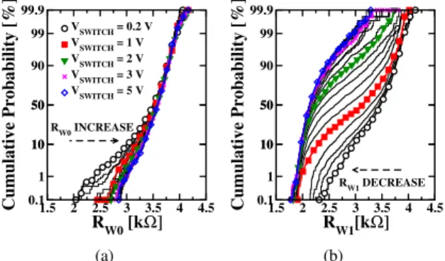
The average resistance and standard deviation measured during switching voltage hysteresis are reported in Fig. 2. Cumulative distribution functions evolution measured during W0 (a) and W1 (b) hysteresis are shown in Fig. 3. The average resistance is strongly reduced after the first step (VSW IT CH= 0.2V ) during W0 hysteresis, whereas W1 hysteresis requires higher voltages: the minimum inter-device variability is ob-tained with VSW IT CH = −5V . The distribution of the resistances measured during W0(RW 0) and W1 (RW 1) as a function of VSW IT CH are shown in Fig. 4. To preliminary evaluate the cells performance, the cycle to cycle variability, and reliability during cycling, 50k W0 and W1 operations been performed on a single page with VF ORCE = 1.4V and |VSW IT CH| = 5V , TF ORCE= 50µs, TSW IT CH= 60µs and Trise/f all= 1µs: Fig. 5 shows the endurance results obtained in terms of average resistance and cumulative probability dis-tributions. The tunnel magnetoresistance (TMR) [9] evolution during cycling has been analyzed in terms of average value and cumulative probability distributions: the results are shown in Fig. 6. The test lasted 30 minutes using full chip W0 and full chip W1 patterns. There are no limits in patterns application on the tested memory. If complex patterns like random device programming or checkerboards are applied on the memory, there are no significant time overheads.
© 2015 IEEE. Personal use of this material is permitted. Permission from IEEE must be obtained for all other uses, in any current or future media, including reprinting/republishing this material for advertising or promotional purposes, creating new collective works, for resale or redistribution to servers or lists, or reuse
of any copyrighted component of this work in other works.
This is the accepted version of the paper. The published version can be found at http://ieeexplore.ieee.org/document/7127367/ The DOI of the published version is: 10.1109/DTIS.2015.7127367
Fig. 1. VSW I T CH hysteresis measured during W0 and W1 operations with VH EAT = 1.4V. -5 -4 -3 -2 -1 0 1 2 3 4 5 VSWITCH [V] 1.8 k 2.0 k 2.2 k 2.4 k 2.6 k 2.8 k 3.0 k 3.2 k 3.4 k 3.6 k 3.8 k Read Resistance [ Ω] WRITE ’0’ WRITE ’1’ µ µ +/− σ
Fig. 2. VSW I T CH hysteresis measured during W0 and W1 operations with
VH EAT = 1.4V. 1.5 2 2.5 3 3.5 4 4.5 R W0 [kΩ] 0.1 1 10 10 50 50 90 99 99.9 Cumulative Probability [%] VSWITCH = 0.2 V VSWITCH = 1 V VSWITCH = 2 V VSWITCH = 3 V VSWITCH = 5 V RW0 INCREASE (a) 1.5 2 2.5 3 3.5 4 4.5 R W1[kΩ] 0.1 1 10 10 50 50 90 99 99.9 Cumulative Probability [%] RW1 DECREASE (b)
Fig. 3. Cumulative density functions measured during VSW I T CHhysteresis
in W0 (a) and W1 (b) operations on fresh device, with VH EAT = 1.4V.
IV. CONCLUSIONS
The preliminary analysis performed on TAS-MRAM demonstrated the validity of the developed ATE, allowing to investigate and understand the hysteresis and endurance properties of the technology in terms of cell-to-cell variability and reliability.
ACKNOWLEDGMENTS
The research leading to these results has (partially) received funding from the European Community’s Seventh Framework Programme FP7 under grant agreement n◦ 619246.
REFERENCES
[1] W. Gallagher et al., “Recent advances in MRAM technology,” in IEEE
VLSI-TSA Int. Symp., April 2005, pp. 72–73.
[2] S. Senni et al., “Power efficient thermally assisted switching magnetic memory based memory systems,” in Int. Symp. on Reconfigurable and
Communication-Centric Systems-on-Chip (ReCoSoC), May 2014, pp. 1–
6.
[3] R. Sousa et al., “Tunneling hot spots and heating in magnetic tunnel junctions,” J. of App. Phys., vol. 95, pp. 6783–6785, 2004.
[4] J. Azevedo et al., “A complete resistive-open defect analysis for thermally assisted switching MRAMs,” IEEE Trans. on Very Large Scale Integration
(VLSI) Systems, vol. 22, pp. 2326–2335, Nov 2014.
0 2 4 1.5 2 2.5 3 3.5 4 4.5 0 0.05 0.1 R W0 [kΩ] V SWITCH [V] PDF 0 2 4 1.5 2 2.5 3 3.5 4 4.5 0 0.05 0.1 R W1 [kΩ] V SWITCH [V] PDF
Fig. 4. 3D plot representing the RW 0 and RW 1 distributions during
VSW I T CH hysteresis with VH EAT = 1.4V.
1 10 100 1k 10k 50k Switching Cycles 1.5 2 2.5 3 3.5 RW0 , R W1 [k Ω] RW0 (µ) RW0 (µ +/- σ) RW1 (µ) RW1 (µ +/- σ) (a) 1.5 2 2.5 3 3.5 RW0,RW1 [kΩ] 1 10 10 50 50 90 99 Cumulative Probability [%] RW1 RW0 1 10 100 1k 10k 50k (b)
Fig. 5. RW 0 and RW 1 measured on a page during 50k cycles with VH EAT = 1.4V, VSW I T CH = 5V (a) and their cumulative probabilities (b). 1 10 100 1k 10k 50k Switching Cycles 40 50 60 70 80 90 100 TMR [%] Max Min µ µ ± σ (a) 40 50 60 70 80 90 100 TMR [%] 0 10 20 30 40 50 60 70 80 90 100 Cumulative Probability [%] 1 10 100 1k 10k 50k (b)
Fig. 6. TMR cumulative density function average value (a) and cumulative probability at different endurance cycles (b).
[5] I. Prejbeanu et al., “Thermally assisted MRAM,” J. Phys.: Condens.
Matter, vol. 19, pp. 165 218–165 241, 2007.
[6] S. Chaudhuri et al., “Design of TAS-MRAM prototype for NV embedded memory applications,” in IEEE Int. Memory Workshop (IMW), May 2010, pp. 1–4.
[7] R. Ferreira et al., “Dynamic thermo-magnetic writing in tunnel junction cells incorporating two GeSbTe thermal barriers,” in IEEE Int. Magnetics
Conf., May 2006, pp. 394–394.
[8] M. Czapkiewicz et al., “Hysteresis loops of magnetically coupled multi-layers - experiment and calculations,” Journal of Magnetics, vol. 9, no. 2, pp. 60–64, Jun 2004.
[9] S. Yuasa et al., “Future prospects of MRAM technologies,” in IEEE Int.