CARBOMAT 2011
90
SHAPING OF DIAMONDS IN 1-D NANOSTRUCTURES AND OTHER STRATEGIES FOR
FABRICATION OF LOW-DIMENSIONAL DIAMOND-BASED COMPONENTS
Maria Letizia Terranova
1,3, Valeria Guglielmotti
1,3, Silvia Orlanducci
1,
Vito Sessa
1, Emanuela Tamburri
1, Francesco Toschi
1,3, and Marco Rossi
2,31
Dept. of Chemical Science and Technology and MINIMAlab,
University of Rome “Tor Vergata”, Roma, Italy
2
Dept. of Fundamental and Applied Sciences for Engineering and CNIS,
University of Rome “Sapienza”, Roma, Italy
3
NanoShare S.r.l., a startup company for human technologies, www.nanoshare.eu, Roma, Italy
*
E-mail: [email protected]
ABSTRACT
The shaping of low-dimensional diamond materials into desired geometries, and the correlated required capability to modify and control the topography of diamond-based systems at the nanoscale, are really challenging and complex tasks, of relevant technological interest. Indeed, ordered arrays of diamond nanowires/nanocylinders are required for the fabrication of advanced photonic and electronic devices, such as stable and robust electron emitters (cold cathodes) able to work in different, and also hostile, environments.
In the present paper we describe some recent methodologies settled in our laboratories for the tailoring of diamond 1-D nanostructures.
1. INTRODUCTION
The outstanding properties, both intrinsic or induced, of diamond materials make them ideal candidates to play a major role in advanced electronic and optoelectronic technologies, for fabrication of sensors, multichip modules and emitting or photoemitting systems. For many applications, however, a nanometric control of the morphological features in terms of size, shape and orientation of the diamond units is strongly required. The objective of our researches is to define methodologies for the tailoring of nanosized diamond materials and their shaping in specific nanoarchitectures . Presently we are developing procedures for the fabrication of elongated diamond 1D structures (nanorods, nanowhiskers, nanopillars, etc) starting from a variety of diamond-based materials .
Two main methodologies are used to achieve the controlled sculpturing of diamond.
The first is a multiscale fabrication process that allows us to produce a variety of self-standing aggregates, up to the mesoscale, with pre-definite shapes starting from colloidal suspensions of ultrananocrystalline diamond powders.
The second process relies on the many new possibilities offered by recent advances in plasma sources and in
particular by the use of a purpose-designed dual-mode MW-RF reactor. The room temperature H-etching processes occurring in the reactor enable the controlled and reproducible fabrication of 1-D nanostructures.
2. EXPERIMENTAL
Surface assisted self-assembling of ultrananocrystalline diamond is obtained starting from colloidal suspension of diamond nanoparticles [1]. For these experiments we use detonation ultrananocrystalline diamond (primary size: 4-5 nm) produced and preliminary de-agglutinated by the Federal Research and Production Center ALTAI (Russia) (Fig.1).
FIGURE 1: HR-TEM image of diamond particles
In our laboratories the received material is further treated following already settled protocols in order to obstacle the re-agglutination processes typical of this class of nanodiamonds. Such nanodiamond assemblies, as well as polycrystalline or B-doped single-crystal diamond plates are used as starting material for the production of diamond nanowires and nanowhiskers. These nanostructures are fabricated by means of the H-induced etching of the diamond phase, accomplished in a Plasma Assisted Chemical Vapour Deposition (PACVD) reactor, where the gas phase is activated by a dual-mode MW/RF plasma.
CARBOMAT 2011
91
3. RESULTS AND DISCUSSION
Differently shaped nanodiamond assemblies (segments, slices) can be selectively obtained by a solution phase method using slurries containing different amounts of dispersed nanodiamonds (Fig.2) [2].
FIGURE 2: Colloidal stable dispersions containing different typologies of nanodiamond particles and self-assembled microstructures obtained from the colloidal suspension.
The nanodiamond assemblies can be also used as templates for diamond growth by CVD. In this case the coating process preserves the architecture of the pristine templates with the formation of a high uniform deposit on all the structures. The coatings are characterized by high phase purity as indicated by Raman and X-ray diffraction characterizations [3].
FIGURE 3: FE-SEM images (above) and Raman and X-ray diffraction (below) of CVD diamond films grown on self-assembled 3-D nanodiamond structures
Fig. 4 shows FE-SEM images acquired before and after the etching treatment of such close-packed flat layers. It can be noted as the etching provoked the generation, in the outermost diamond sheets, of a very complex structure shaped like an array of vertically aligned whiskers resulting from the erosion at the nanoscale of the pristine deposit [4].
FIGURE 4: FE-SEM images of a self-assembled 3-D nanodiamond structure acquired (a) before and (b) after the etching treatment.
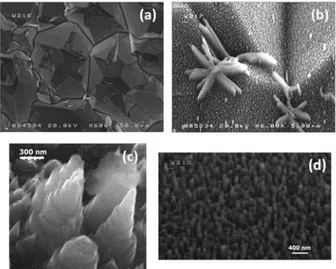
Nanocolumns and nanopillars are instead obtained starting from polycrystalline diamond films prepared by CVD (Fig. 5).
FIGURE 5: FE-SEM images of polycrystalline diamond film acquired (a) before and (b) after the etching treatment; (c) and (d) magnifications of the deposit.
The structural characterizations performed on a series of samples indicate that the etching process induced by H ions does not modify the lattice parameters of the diamond phase, that still retains its outstanding properties (Fig.6) [3].
FIGURE 6: Typical Raman spectra and RHEED pattern of diamond systems subject to etching treatments.
It is worthnoting that the I/V measurements of plasma-treated diamond samples evidenced that the H-induced etching process substantially lowersthe resistivity of the material. Moreover, Field Emission measurements indicate that the elongated nanocrystalline diamond deposits are very efficient electron emitters in terms of reproducibility, current stability under medium vacuum and lack of arcing (Fi. 7). These nanostructures are highly
CARBOMAT 2011
92
recommended for the assembling of cold cathodes when amaterial enduring harsh operation conditions is required.
FIGURE 7: Typical I/V data and Fowler-Nordheim plot of the Field Emission characterizations carried out before and after the etching process on a diamond sample.
4. CONCLUSIONS
The entire class of nanosized diamond represents nowadays one of the most promising and exciting field of research, not only for challenging technological applications, but also for investigation of the aggregation/etching mechanisms that lead to specific nanoarchitectures with different dimensionalities.
The room temperature H-etching processes occurring in our MW-RF reactor enable the reproducible fabrication of a series of tailored diamond-based devices, where the location and the shaping of the diamond deposits can be easily controlled.
These low-dimensional diamond structures represent not only a viable alternative for easy and low-cost manufacturing of diamond micro-and nano-components for the next-generation devices, but also for different and advanced applications in the field of bioscience (as biosensing and biolabeling) where inert materials and specifically shaped surfaces are needed.
5. REFERENCES
[1] V.Y. Dolmatov, Russian Chemical Reviews 70 (2011) pp. 607-626
[2] M.L. Terranova, D. Manno, M. Rossi, A. Serra, E. Filippo, S. Orlanducci, E. Tamburri, Crystal Growth & Design 9 (2009) 1245
[3] M.L. Terranova, S. Orlanducci, E. Tamburri, V. Guglielmotti, F. Toschi, D. Hampai, M. Rossi, Nanotechnology 19 (2008) 415601
[4] S. Orlanducci, F. Toschi, V. Guglielmotti, E. Tamburri, M. L. Terranova, M. Rossi, Nanosci. Nanotechnol. Lett. 3 (2011) 83