Abstract—This paper reports about the performances of single
crystal diamond (SCD) detectors operated at high temperature (up to 200 C) and irradiated with alpha particles. Two different types of SCD detectors were studied: a) SCD of commercial type; b) SCD produced at Rome “Tor Vergata” University and characterized by a layered structure.
The first measurement of the response function vs. temperature of commercial SCD detector irradiated with 14 MeV neutrons and heated up to 140 C is also reported.
The measurements pointed out the superior performance of di-amond with respect to other detectors (e.g., silicon) when operated at high temperature. However, the present work also pointed out that a diamond detector assembled to operate at room tempera-ture can suffer from mechanical stress when operated at high tem-perature. The results indicate that, with a proper design, diamond detectors can be suitable for operation at high temperature.
Index Terms—Artificial single crystal diamond, high
tempera-ture detectors, neutron detectors, neutron spectrometry, radiation detector.
I. INTRODUCTION
R
ADIATION detectors operate routinely at room temper-ature (300 K) and their characteristics and performance under this working condition are usually well established. How-ever, in some applications it could be required of the detectors to operate at a temperature much higher than 300 K. This is the case of the neutron detectors to be located in the International Thermonuclear Experimental Reactor (ITER) [1]. ITER is the next generation fusion tokamak presently under construction in Cadarache (France) as a joint effort among seven partners (EU, USA, RF, China, Japan, Korea, India).Among the many challenging problems to be faced in ITER, the detectors to be used to monitor and diagnostic the burning plasma should be able to withstand very harsh working
condi-Manuscript received December 15, 2011; revised March 20, 2012 and July 20, 2012; accepted July 23, 2012. Date of publication September 17, 2012; date of current version October 09, 2012.
M. Angelone, M. Pillon, G. Prestopino, and F. Sarto are with the Associazione Euratom-ENEA sulla Fusione, ENEA C.R. Frascati, CP 65, I-00044 Frascati, Italy (e-mail: [email protected]).
N. Fonnesu was with the University of Rome “La Sapienza”, and is now with the University of Padova, Padova, Italy (e-mail: [email protected]).
E. Milani, M. Marinelli, C. Verona, and G. Verona-Rinati are with the De-partment of Industrial Engineering, Universitá degli Studi “Tor Vergata” Rome, 1-00100 Rome, Italy (e-mail: [email protected]).
Color versions of one or more of the figures in this paper are available online at http://ieeexplore.ieee.org.
Digital Object Identifier 10.1109/TNS.2012.2210735
tions mainly due to high neutron and gamma fluxes, EM fields and high temperature, the latter due to the huge radiation field.
To study the plasma performances in ITER a number of dif-ferent diagnostics systems are foreseen. Most of them are lo-cated in the so-called diagnostics ports which are large hori-zontal or vertical penetrations available in the tokamak struc-ture (vacuum vessel). These ports are rather harsh environments since from one side they look directly to the plasma, thus huge neutron and gamma fluxes penetrate them. The bottom side of the port is instead heavily shielded to avoid radiation outside the tokamak. The diagnostic instrumentation located inside the port must thus withstand such a harsh environment.
One of the most important diagnostic apparatus in ITER will be the so-called neutron camera, a system devoted to measure the neutron emission from the burning plasma from which rel-evant plasma parameters can be derived. The neutron camera is made of a number of narrow-bore collimators (1–2 cm diam-eter) several meters long. At one end they look at the plasma, at the other end neutron detectors will be located. The detectors will be used for simultaneous measurement of neutron spectra and total neutron production, the latter is obtained after a proper reconstruction of the plasma emission profile by tomography methods.
The neutron camera is located inside one of the equatorial ports of the ITER tokamak (Fig. 1) and its operational conditions are very severe being characterized by a high flux of radiation (e.g., neutron flux n/cm s, at the collimator end [2], while the gamma flux is about ten time higher) and high temperature (100–120 C). These conditions require a proper selection of the neutron detectors to be located inside the neutron camera since the detectors must also ensure good spectrometric performances even at high temperature. Among the possible candidates (e.g., scintillators), artificial single crystal diamond (SCD) detectors seem very promising.
Diamond has many outstanding properties [3] and the radi-ation tolerance, the high energy resolution ( 0.5% at FWHM measured using 5.48 MeV alphas from Am) and the excel-lent neutronic spectrometric properties [4] as well as the capa-bility to operate at high temperature (shows the highest thermal conductivity, 22 Wcm K ) are beneficial for detectors made of diamond.
Diamond detectors are studied since many years for appli-cation in nuclear fusion devices. They have been proposed and successfully tested at the JET tokamak for measuring neutrons as well as UV and soft X-ray [5], [6], showing excellent perfor-mances and capability to withstand the tokamak working con-0018-9499/$31.00 © 2012 IEEE
Fig. 1. The ITER radial (RNC) and vertical neutron camera (VNC).
ditions. However, their behavior at high temperature has been studied little so far [7]–[11] and most of the available literature deals with polycrystalline films.
This paper represents one of the first attempts to study arti-ficial SCD detectors under high temperature conditions (up to 200 C), similar to the one encountered at the actual work at the tokamak reactor. It reports about the influence of temperature on spectrometric and time dependent performances of two dif-ferent types of artificial SCD detectors.
The first measurement (to the authors knowledge) of the re-sponse function versus temperature of a commercial SCD de-tector irradiated with 14 MeV neutrons and heated up to 140 C is also reported.
II. DIAMONDDETECTORS
The work reported hereafter was performed by comparing the behaviour of two different types of artificial SCD detectors:
a) commercial SCD film provided by Diamond Detectors Ltd
(DDL, UK) which is made of a thick layer (500 m) of intrinsic diamond. DDL did not provide operational detectors since metallic contacts were deposited by the authors (Section II-A);
b) SCD detector produced at Rome “Tor Vergata”
Univer-sity and characterized by a layered structure and Al contact (Section II-B).
It is important to mention that both the used detectors were the same as those used so far by our team at room temperature, that is made with the diamond crystal housed in an Aluminium casing and equipped with a standard SMA connector. In both cases the connection between the SCD upper metallic contact and the SMA connector was made by a metallic wire bounded by pure tin solder.
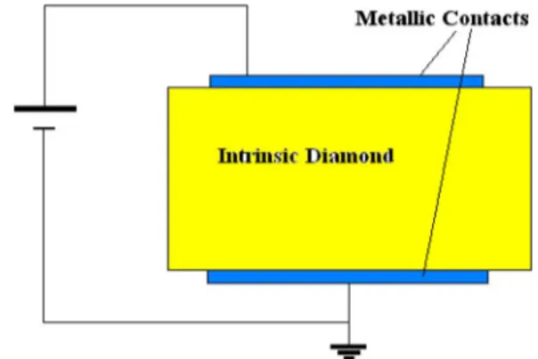
A. Commercial SCD Detector
The commercial SCD used in this work (Fig. 2) was made using an artificial single-crystal diamond 500 m thick and
mm in area.
Fig. 2. Lay-out of a commercial SCD detector.
Two metallic contacts were deposited at ENEA on each side of the crystal, by DC sputtering. The coated areas were cir-cles of 3 mm diameter and were entirely contained within the edges of the substrate by masking the substrate with kapton during deposition. The DC sputtering system was a MED20 coating facility manufactured by Baltec, equipped with three targets, to allow sequential deposition of multilayer films during the same vacuum process. Before film deposition the substrates were chemically cleaned by ethylic alcohol and left to degas and dry in air. Actually, such a pre-deposition thermal treatment resulted to be critical to prevent film buckling and detaching during high temperature operation.
Two different types of contacts made of Pt and Ti respec-tively were deposited and studied to understand whether dif-ferent metal contacts could affect the behavior at high temper-ature. The Pt contact consisted of a single film, 130 nm thick, directly deposited onto the diamond substrate. In the other case, the first Ti layer (about 60 nm thick) adjacent to the substrate was over-coated by a top Pt thin layer (about 10 nm thick) to prevent Ti oxidation. The lower contact was grounded by mean of annealed silver paint.
Film thicknesses were measured in situ by a profilometer, which was previously calibrated by Scanning Electron Mi-croscopy.
B. Layered SCD Detector
The structure of the layered diamond detector (Fig. 3) was obtained by a two steps deposition process [13]. A conductive boron-doped diamond homoepitaxial layer, used as backing contact, is deposited at first by chemical vapor deposition method (CVD) on a commercial synthetic high pressure high temperature (HPHT) type Ib single crystal diamond substrate, mm in size. The boron doped layer is a few mi-crons thick (5–10 m , its boron concentration was estimated
to be about cm . After that a nominally intrinsic
diamond layer (detecting region) is homoepitaxially grown on the doped one by using a different apparatus to avoid any boron contamination. Its thickness can vary from a few microns up to more than 200 microns. For this work, a thickness of 55 m was used. After the growth, each diamond layer has been oxidized by isothermal annealing at 500 C, for 1 h in air, in order to re-move the conductivity of the as-grown hydrogenated diamond surface. Finally, a circular metal electrode (Aluminum), about
Fig. 3. Structure of the layered SCD detector.
3 mm in diameter and 100 nm in thickness was deposited on the diamond surface by thermal evaporation [14], [15].
Annealed silver paint (1 h at 500 C in air) was utilized to pro-vide an ohmic contact with the B-doped layer. The Al-SCD was operated in reverse biased mode with a positive voltage on the top contact while the boron doped contact is grounded (Fig. 3). It is worthwhile to mention that the presence of a built-in po-tential of about 1.5 eV due to the metal/diamond junction [16] allows the detector to operate without any applied external bias.
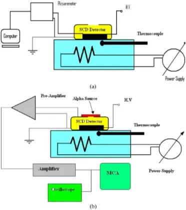
III. EXPERIMENTALSET-UP ANDMEASUREMENTS All the SCD detectors used in this work were studied using the same experimental approach: 1) for each detector the dark current was firstly measured as function of both temperature and applied external bias by using a picoammeter (Fig. 4(a), Section IV-A); 2) the spectrometric properties were investigated by means of alpha sources. In this case 5.5 MeV alphas from Am source (activity 5.9 kBq) or a triple alpha source
ob-tained by a mixture of Pu, Am and Cm (main alphas
lines: 5.3 MeV, 5.5 MeV and 5.85 MeV respectively and total activity 5.5 kBq) were put on top of the detector and used to irradiate the SCDs and study their behavior versus temperature (Fig. 4(b)). Further studies were performed using 14 MeV neu-trons.
For all the used detectors the parameters investigated are: a) position of peak centroid, b) peak area and c) peak resolution (FWHM).
All measurements were performed heating the SCD detector by mean of an electrical heater controlled by a current generator. A thermocouple monitored the working temperature which
was kept in the range C.
The measurements reported in this paper were performed in air (distance source-detector 4.5 mm). A collimator (3 mm in diameter) was used.
Pulse height spectra (PHS) of the used alpha sources were recorded by a multichannel analyzer (MCA) at increasing tem-perature and up to 200 C, in steps of 20 C. The count rate was of 180 cps (at room temperature). Each measurement lasted 1000 sec to allow for a suitable counting statistics of the mea-sured peak area. The peak area was calculated by a straightfor-ward fitting procedure with peak background subtraction. Typ-ical uncertainty for the measured net peak area was of the order
of 3%.
Fig. 4. (a) Lay-out of the experimental set-up for current measurements; (b) Lay-out of the experimental set-up for spectrometric measurements.
For the commercial detector all the above mentioned mea-surements were repeated twice by changing the Pt contacts into Ti. This was obtained by removing the Pt contacts and depositing, still by DC sputtering (see Section II-A) the new Ti contacts on the same SCD diamond after new annealing of the SCD film at 500 C for one hour in air
IV. RESULTS
A. Dark Current Measurement
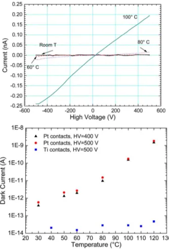
Preliminarily to the measurements to be discussed in Section IV-B the dark current versus temperature was measured by using a picoammeter (Keithley Mod. 6517A). The applied bias (H.V.) was in the range from 500 V to 500 V. The measurements were performed in air.
The results for the commercial SCD detector with Pt contacts are reported in Fig. 5(a) and (b). In Fig. 5(a), the dark current curve is almost symmetric with respect to the sign of the applied H.V. In Fig. 5(b) the dark current vs. temperature (for the mea-surement with bias voltage of 400 and 500 V respectively) is reported.
Dark current measurements provided many insight about the response of the detector as a function of temperature. It was noted that the detector is almost insensitive to temperature up to 80 C. Above this temperature the dark current increases, and
for –150 C the measured current is so high that it
saturates the used instrument. As a consequence of the above phenomenon, during the PHS measurement at increasing tem-peratures, an increase in detector noise and dead time of the electronics chain was always observed which resulted in almost
Fig. 5. a) Commercial SCD with Pt contacts: I-V plot at various temperatures; b) Dark current versus temperature for commercial detector with Pt contacts biased at two different H.V. The figure also reports the dark current measured by SCD with Ti contacts for H.V V.
As far as the commercial SCD detector with Ti contacts is concerned, we still observed a rather symmetric curve as a func-tion of the biasing voltage, however, in the investigated temper-ature range (up to 120 C) the value of the dark current resulted much lower than that measured for Pt contacts (Fig. 5(b)).
The dark current of the layered detector resulted lower than that of the commercial detector. At room temperature and up to 80 C the measurements were at the lower limit of the used electrometer sensitivity. Above 100 C we observed again the behavior already discussed for the commercial detector with Pt contacts getting saturation at a slight lower temperature
C . The curve is now asymmetric with respect to the H.V. indicating that the layered detector behaves as a rectifying de-vice.
B. Alpha Source Measurements
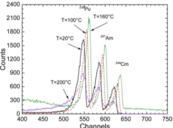
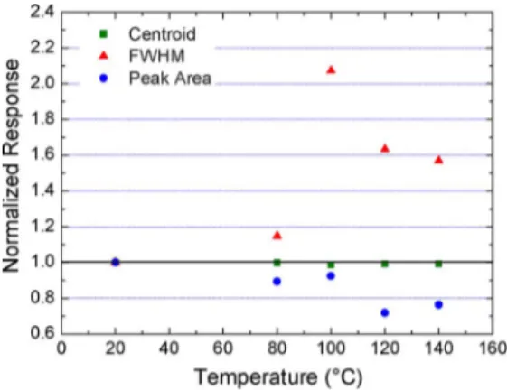
The results for the commercial SCD detector with Pt con-tacts are summarized in Fig. 6 where the behavior of: a) peak centroid, b) peak area and c) peak resolution (FWHM) versus temperature are reported.
All data presented in this paper are normalized to data col-lected at room temperature (20 C). This gives insight about the detector behavior versus temperature. The measurements were
Fig. 6. Peak centroid, peak area and FWHM vs. temperature for commercial SCD detector with Pt contacts H.V V .
Fig. 7. Peak area vs. temperature at different H.V. for commercial SCD de-tector with Pt contacts.
Fig. 8. Peak resolution (FWHM) vs. temperature at different H.V. for commer-cial SCD detector with Pt contacts.
also repeated at several H.V. and the results are reported in Fig. 7 and 8.
Fig. 7 seems to indicate that the H.V. affects the detector re-sponse. Indeed, the figures show that the peak area and the peak centroid change a few percent at 800 V, while there is an in-crease 20% at 400 V. Similar results were observed also for the commercial SCD detector with Ti contacts. However, in this case the variations of the various peak parameters between the highest and lower biasing voltage are reduced to a few percent.
Fig. 9. Peak centroid, peak area and FWHM vs. temperature for layered de-tector with Al contact and H.V. V.
Fig. 10. Peak area vs. temperature at different H.V. for layered detector.
Fig. 11. FWHM vs. temperature at different H.V. for layered detector. The same quantities reported above for the commercial de-tector were studied for the layered dede-tector. The results, nor-malized to data collected at room temperature, are shown in Figs. 9 to 11.
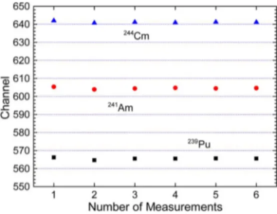
Long lasting measurements were also performed. In this case the PHS was acquired six times consecutively (each measure-ment lasted 500 sec), keeping the detector at 120 C (Fig. 12). Good stability was observed for all the used detectors.
Last, but not least, during the various measurements reported above the pulse produced by the used detectors were routinely monitored and recorded by an oscilloscope.
In literature it is reported that the signal produced in diamond is formed by the combination of a fast and a slow component
Fig. 12. Long lasting measurement at C: peak centroid vs. number of consecutive measurements (each one lasting 500 s) for the triple alpha source. Data refer to SCD detector with Pt contacts and H.V. V.
Fig. 13. Comparison of pulses recorded by oscilloscope at 20 C (Top) and at 150 C (Bottom) for SCD with Ti contacts H.V V .
[8]–[11]. The latter has been associated to hole trapping-detrap-ping and a reduction of this slow component as temperature increases has been observed, indicating a more efficient trap-ping-detrapping process of holes at high temperature [11]. In our case no significant variation of the pulse shape with temper-ature, for a fixed external bias, was observed for the commer-cial detector. In particular, the slow component was not present (Fig. 13). We mention that a similar result was already reported in [12] for a detector produced by the same company which pro-vided us the diamond film. The temperature range investigated in [12] was from 0 C up to 30 C.
However, the increase of electrical noise was clearly visible and measurable in the PHS spectra as function of temperature and for C noise increased steeply as well as the dead
time. For C we observed the paralyses of the
elec-tronics chain with a sudden reduction of both peak area (Fig. 14) and spectrometric performance of the detector. This behavior
Fig. 14. Effect of temperature on peaks area of a triple alpha source. Mea-surement performed with the commercial detector with Pt contacts operated at H.V. V. The sudden reduction of the peaks at 200 C is evidenced as well as the noise increase in the PHS spectrum.
Fig. 15. Commercial SCD detector with Ti contacts: comparison between triple alpha spectra measured at two different H.V. (data refer to detector operated at room temperature).
was observed for all the used detectors, but for the layered one it occurred at a slightly lower temperature C .
C. 14 MeV Neutron Measurements
The response functions of a commercial diamond detector ir-radiated with neutrons from 7 up to 20 MeV were already re-ported for detectors operated at room temperature [4].
The response function of a SCD detector irradiated with 14 MeV neutrons and operated from room temperature up to 140 C was also measured in this work. The commercial SCD detector with Ti contacts was used. The choose of Ti contacts was sug-gested by the results reported in sect.III.A. It was noted that with Ti contacts a lower level of noise is generated at high temper-ature. It was also noted that Ti contacts allow to bias the SCD detector at a lower voltage than Pt contacts without loosing the detector performance (Fig. 15).
The applied voltage was 100 V (0.2 V m). This biasing voltage was used because at higher values the detector was not longer operating in a satisfactory way (too many noise, see. Section V).
In the authors’ knowledge this is the first attempt to use a SCD detector at high temperature under neutron irradiation. The measurements were performed at the 14 MeV Frascati neutron generator (FNG) [17].
Fig. 16. a) Response function of commercial SCD detector with Ti contacts irradiated at FNG with 14 MeV neutrons and kept at room temperature. Biasing voltage 100 V; b) C n Be peak measured at different temperatures and
H.V. V.
To better understand the results a few words about the neu-tron-carbon interaction with (14 MeV) neutrons are useful.
A typical PHS recorded in this work using the commercial SCD detector with Ti contacts while irradiated at room tempera-ture with 14 MeV, is reported in Fig. 16(a). It is characterized by a sharp peak produced by the C n Be reaction (threshold 5.7 MeV) due to the fully absorbed energy of the and Be ions in the detector. For 14 MeV neutrons this peak is centered at 8.3 MeV.
Another important reaction in Carbon is C n (the
so-called carbon break-up reaction) which produces the con-tinuum on the left side of the main peak. The concon-tinuum extends to very low energies since other reactions (e.g., inelastic scat-tering) occur in carbon.
Fig. 16(b) shows in detail the measured C n Be peak at various temperatures (20 C, 80 C, 100 C and 140 C). Fig. 17 reports the measured FWHM, peak area and centroid vs. tem-perature for the C n Be peak.
V. DISCUSSION
The results reported above seem indicate that diamond detec-tors can operate at high temperature despite a number of effects need to be better understood and some technical problems are to be faced and solved.
The results reported in Figs. 6 to 11 show that the response of both commercial and layered SCD detectors vs. temperature is almost the same, at least in the temperature range investigated in this work. The various parameters investigated show always the same behavior, the peak resolution (FWHM) seems to improve slightly with temperature while the peak position shifts a few channels. The peak area is in turn affected by temperature by no more than 25% when the detector is operated at low bias
V m , but varies within 10% for H.V V m.
However, it seems that the commercial detector can withstand higher temperature than the layered one. Indeed, for C
Fig. 17. FWHM, centroid and area of the C n Be main peak versus tem-perature measured for SCD with Ti contacts H.V V . Data normalized to room temperature.
a loss of performances of the layered detector was observed. In particular the peak’s area and the peak’s resolution (FWHM) changed dramatically.
Among the various problems encountered, the most critical seems to be the increase of the detector noise above 100 C. As already said, noise increases with temperature up to prevent the detector operation for C. It is not clear yet whether the origin of this problem is intrinsic to the detector or it is also due to its structure (contacts, connector, cable, etc.) not yet op-timized to operate at high temperature and so contributing to thermal noise generation.
In diamond there are (relative) shallow traps in the energy gap where carriers are trapped and de-trapped continuously [8], [11]. This process is enhanced by temperature as already observed for polycrystalline diamond [11], although this is not directly applicable to single crystal diamond owing with the different structure of traps for the two crystals. As already mentioned in Section IV-B, in literature it is reported that the signal produced by diamond is formed by the combination of a fast and slow component [8]–[11]. The latter has been associated to hole trap-ping-detrapping and it has been also observed a reduction of this slow component as temperature increases, indicating a more ef-ficient trapping-detrapping process of holes at high temperature [11]. Responsible of these effects are relatively shallows traps identified by various authors [8], [12] to be in the energy range 0.29–0.39 eV. As reported in Section IV-B, such effects were not observed with our commercial SCD detector.
In the effort to find an explanation to the noise increase, the latter can be attributed to the decrease of the hole mobility with temperature increase [18] which can produce polarization ef-fects in the active region. These polarization efef-fects can be en-hanced at the interface detector-metal contact due also to the re-duced carrier mobility in metal with temperature. This, in turn, produces accumulation of charges in the region close to the metal contact, which can lead to a reduction of the detector per-formance at high temperature.
Another observed effect was the shift toward higher channels (energies) of the position of the peak centroid, that is a slight improvement of the charge collection efficiency (CCE, see e.g., Fig. 6). This effect was always observed for C, that is before the above discussed paralysis of the detector occurs.
duced charge and the total charge (electron-hole pairs) produced
by the impinging radiation . If the charge inside
the detector increases, e.g., due to reduced hole trapping caused by thermal excitation or also for longer transit time due to the above mentioned decrease of hole mobility, increases so, increases as well. Indeed in [10] this is demonstrated for the case of a polycrystalline film by mean of simulation. The latter foreseen an increase of the collection efficiency up to very high temperatures C , while we observed a sudden decrease above 160–170 C. This experimental fact can suggest the al-ready mentioned possibility that also other or external causes have to be considered for the observed noise.
The results obtained with 14 MeV neutrons needs a comment as well. The results of Figs. 16 and 17 show that the spectrom-etry performances are not lost for C. Above this tem-perature the peak produced by the C n Be reaction, which is of interest in neutron spectrometry, shows degradation which increases with temperature. Both energy resolution and peak area change (Fig. 17) and again the electronics noise increases with temperature. The measurements at 200 V were possible up to 100 C while with an external bias of 100 V the measure-ments were possible up to 140 C. We wonder whether this could depend also upon the higher count rate ( 2500 cps) respect to alpha measurements which could increase ionization and car-riers production.
Another possible effect is that due to prompt gammas which are always present during neutron irradiation. Their presence must be considered since the count rate as well as noise in the low energy part of the PHS increase.
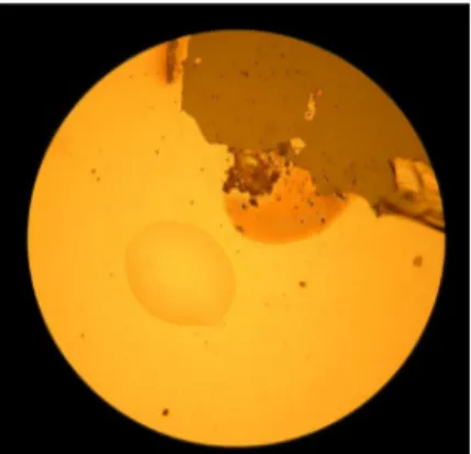
Last, but not least, another observed phenomenon was the damage of the electrical contacts for the detectors operated at high temperature. Pictures of the metallic contacts taken using an optical microscope clearly evidenced their damage (forma-tion of small bubbles and metal detachment, Fig. 18). This was observed (before neutron irradiation) after long operation (sev-eral hours) at temperatures around 140–150 C. A possible ex-planation of this effect can be the different thermal expansion coefficients of metals and diamond, with the former material having a thermal expansion coefficient much higher than dia-mond. This produces friction and thus can lead to the observed phenomena. Some simulations based upon the use of thermo-mechanical code ANSYS [20] were performed which confirmed such a hypothesis.
It ought to be recalled that the used detectors were as those routinely used at room temperature. The results clearly indicates that the “standard” detector configuration discussed in Section II can be used to operate up to 130–140 C. However, at
tem-Fig. 18. Picture (taken using an optical microscope) of the Pt contact after op-eration at high temperature. The contact damage is well evidenced.
perature higher than 130–140 C it is necessary to modify the detector structure. In particular the backing contact cannot be made with the used conductive glue and mechanical or spe-cial welded contacts are necessary. The same applies to detector chassis, connector and cable. Chassis made of tungsten or alu-mina can be useful while mineral cables and special (mineral) connectors developed to operate at high temperature and high radiation fields and already available on the market, will be nec-essary. This is particularly true for operation in an harsh envi-ronment such as that expected in ITER.
VI. CONCLUSION
The response of two different single crystal diamond detec-tors was studied as function of temperature using both alphas particles and 14 MeV neutrons.
In their present configuration the used diamond detectors demonstrate good spectrometric and electric performances for operation up to 130–140 C. At higher temperature the electronics noise mainly due to thermal effects tends to increase
steeply and paralyzes the electronics for C. Some
hypothesis about the origin of this noise were addressed in the paper but it is still unclear whether also external causes, such as the mechanical and electrical (contacts, cables, connector) structure of the detector, can affect the response of the diamond detector operating at high temperature.
For the commercial detector no substantial difference in the behavior at high temperature was observed by changing the metal contacts from Pt into Ti, but Ti contacts resulted in lower noise and a much smaller dark current respect to Pt contacts and were preferred for 14 MeV neutron measurement at high tem-perature.
Further studies at higher temperatures are necessary but this requires to build detectors with chassis, connector and cable suitable to withstand high temperature in order to avoid or at least to reduce the influence of external causes on the observed effects. For the present available artificial SCD diamond detec-tors it can be concluded that they can withstand operation at
and M. L. Sergi, “Experimental response functions of a single-crystal diamond detector for 5–20.5 MeV neutrons,” Nucl. Instrum Meth.
Phys. Res., vol. A-640, pp. 185–191, 2011.
[5] M. Angelone, D. Lattanzi, M. Pillon, M. Marinelli, E. Milani, and A. Tucciarone et al., “Development of single crystal neutron detectors and test at JET tokamak,” Nucl. Instrum. Meth. Phys. Res., vol. A595, pp. 616–622, 2008.
[6] M. Angelone, M. Pillon, M. Marinelli, E. Milani, G. Prestopino, and G. Verona-Rinati et al., “Single crystal artificial diamond detectors for UV and soft X-rays measurements on JET thermonuclear fusion plasma,”
Nucl. Instrum. Meth., vol. A623, pp. 726–730, 2010.
[7] Y. Tanimura, J. Kaneko, M. Katagiri, Y. Ikeda, T. Nishitani, H. Takeuchi, and T. Iida, “High temperature operation of a radiation detector made of a type IIa diamond single crystal synthesized by HPHT method,” Nucl. Instrum. Meth., vol. A443, pp. 325–330, 2000. [8] A. Balducci, M. Marinelli, E. Milani, M. E. Morgana, G. Prestopino, M. Scoccia, A. Tucciarone, and G. Verona-Rinati, “Trapping-detrap-ping defects in single crystal diamond films grown by chemical vapor deposition,” Appl. Phys. Lett., vol. 87, p. 222101, 2005.
[9] R. D’Alessandro, F. Hartjes, S. Lagomarsino, and S. Sciortino, “Influ-ence of temperature on the response of high quality polycrystalline dia-mond detectors,” Nucl. Instrum. Meth., vol. A570, pp. 303–307, 2007. [10] L. Milazzo and A. Mainwood, “Modelling of diamond particle detec-tors: Temperature dependence of the trapping detrapping phenomena,”
Diam. Rel. Mater., vol. 12, pp. 658–661, 2003.
[11] M. Marinelli, E. Milani, A. Paoletti, G. Pucella, A. Tucciarone, G. Verona-Rinati, M. Angelone, and M. Pillon, “Analysis of traps in high quality CVD diamond films through the temperature dependence of carrier dynamics,” Diam. Rel. Mater., vol. 12, pp. 1733–1737, 2003. [12] A. Lohstroh, P. J. Sellin, S. G. Wang, A. W. Devies, and J. M. Parkin,
“Mapping of polarization and detrapping effects in syntetic single crystal chemical vapor deposited diamond by ion beam induced charge imaging,” J. Appl. Phys., vol. 101, p. 063711, 2007.
[13] M. Marinelli, E. Milani, G. Prestopino, M. Scoccia, A. Tucciarone, G. Verona-Rinati, M. Angelone, D. Lattanzi, and M. Pillon, “High perfor-mance LiF—Diamond thermal neutron detector,” Appl. Phys. Lett., vol. 89, p. 143509, 2006.
[14] P. Gonon, A. Deneuville, E. Gheeraert, and F. Fontane, “Influence of annealing on the resistance of polycrystalline chemically vapour de-posited diamond films: A surface chemical effect,” Diam. Rel. Mater., vol. 3, p. 654, 1994.
[15] N. Jian and T. Ito, “Electrical properties of surface conductive layers of homoepitaxial diamond films,” J. Appl. Phys., vol. 85, p. 8267, 1999. [16] S. Almaviva, M. Marinelli, E. Milani, G. Prestopino, A. Tucciarone,
and C. Verona et al., “Chemical vapor deposition diamond based mul-tilayered radiation detector: Physical analysis of detection properties,”
J. Appl. Phys., vol. 107, no. 1, p. 014511, 2010.
[17] M. Martone, M. Angelone, and M. Pillon, “The 14 MeV Frascati Neu-tron generator,” J. Nucl. Mater., vol. 63, p. 1661, 1993.
[18] N. Tranchant, M. Nesladek, D. Tromson, Z. Remes, A. Bogdan, and P. Bergonzo, “Time of flight study of high performance CVD diamond detector devices,” Phys. Stat. Sol. (a), vol. 204, p. 3023, 2007. [19] S. Ramo, “Currents induced by electron motion,” Proc. IRE, vol. 27,
no. 9, pp. 584–585, 1937.
[20] ANSYS Mechanical APDL Coupled-Field Analysis Guide. [Online]. Available: http://www1.ansys.com/customer/documentation/130/ams-cou.pdf