Anomalous
optical and electrical recovery processes
of the photoquenched
EL2 defect produced
by oxygen and boron ion implantation
in gallium
arsenide
J. Samitier, S. Marco, A. Perez-Rodn’guez, and J. FL Morante
L. C. M. M. Departament de Fisica Aplicada i Electrbnica, Universitat de Barcelona, Avda. Diagonal 645-647, Barcelona 08028, Spain
P. Boher and M. Renaud
Laboratoire d%lectronique Philips, 3 Avenue Descartes, BP 15-94450, Lime&Brevannes, France (Received 30 July 1991; accepted for publication 24 September 1991)
The optical and electrical recovery processes of the metastable state of the’EL2 defect
artificially created in n-type GaAs by boron or oxygen implantation are analyzed at 80 K using optical isothermal transient spectroscopy. In both cases, we have found an inhibition of the electrical recovery and the existence of an optical recovery in the range 1.1-1.4 eV, competing with the photoquenching effect. The similar results obtained with both
elements and the different behavior observed in comparison with the native EL2 defect has been related to the network damage produced by the implantation process. From the different behavior with the technological process, it can be deduced that the electrical and optical anomalies have a different origin. The electrical inhibition is due to the
existence of an interaction between the EL2 defect and other implantation-created defects. However, the optical recovery seems to be related to a change in the microscopic
metastable state configuration involving the presence of vacancies.
INTRODUCTION
It is well known that the EL2 defect in GaAs presents an interesting optical property known as the photoquench- ing effect. Basically, this feature is attributed to the exist- ence of two different atomic configurations, labeled stable and metastable, for the same charge state of the defect. The main characteristic of the metastable state is that it does not show optical response when the sample is irradiated with photons in the energy range about 0.9-1.4 eV at tem- peratures below 120 K (for a review of the EL2 properties see Refs. 1 and 2). This behavior has been observed by different experimental techniques, such as photolumines- cence, photoconductivity, photocapacitance, or infrared absorption and has been suggested as an accurate method to determine the presence of the EL2 defect in the gallium arsenide as-grown or after irradiation or implantation processes.3
Two mechanisms have been proposed by different authors”’ in order to achieve the complete transfer from the metastable to stable configuration: (i) thermal mecha- nism, with an activation energy of about 0.3 eV; (ii) Elec- trical mechanism, which is induced by free carriers injec- tion. Moreover, a third partial recovery mechanism has been reported by several authors when the samples are optically irradiated with photons of given energies.h7 However, these works disagree in some important aspects such as the amount of optical recovery and their spectral dependence.
These differences, in addition to other discrepancies observed in the characteristic parameters of the EL2 cen- ter, measured by several techniques from different samples, have led to the concept of the EL2 family as a family of similar defects with different microscopic configurations.“78
We have to remark that, in spite of many works devoted to the EL2 defect, its microscopic structure is unknown, al- though it is generally assumed that the EL2 involves the arsenic antisite defect, Asoa, as the* main9?i0 or exclusive component.‘1-13 The existence of defect interactions be- tween an essential EL2 and other structural defects or im- purities has been suggested to explain the discrepancies observed in the defect properties. In this way, Manasreh and Fisher’ have recently pointed out that differences in the photoinduced recovery process of the metastable state can be related to the presence and nature of other defects and impurities surrounding the EL2 defect. Likewise, Parker and Bray14 have claimed that the variety of thermal recovery processes in different samples can be explained by the possibility that metastable defects can exist with struc- tural modifications, possibly related to the impurities, and Desnika, Desnika, and Santic,” from the analysis of the photoconductivity and thermally stimulated current in semi-insulating @I) GaAs, suggest EL2 as a gettering cen- ter for other native defects or impurities.
On the other hand, although the EL2 is a native defect in the material grown by Bridgman and Czochralski tech- niques, different authors have reported the artificial cre- ation of deep defects with characteristics very similar to those of the EL2 center by irradiation of neutrons or im- plantation of different ions (As, Ga, 0, Ne, B) followed by high-temperature thermal annealing (
T > 600 "C) . 'w'
In these cases, the activation energies of the emission rate and the photoquenching spectra are also found to show differ- ences in relation to the starting EL2 defect. These depend on the characteristics of the starting material, the im- planted specimen, and the annealing treatment. More re- cent works have reported the strong ability of the EL2center created by implantation processes for its interaction with shallower defects, questioning the need for a thermal treatment for the creation of the defect.19
Therefore, an interesting approach to achieve a clearer understanding of the nature of the EL2 defect can be ob- tained from the analysis of the properties of the EL2-like centers produced by ion implantation, as well as their in- teraction with shallower defects also created during these processes. In this framework, we present the results on the characterization of the photoquenching recovery of the EL2 center created by means of the ion implantation of two different elements, oxygen and boron. The analysis has been done in a comparative way in relation to the behavior observed in as-grown material, where EL2 is a native de- fect.
SAMPLES AND EXPERIMENTAL DETAILS
Oxygen-implanted samples have been obtained using as starting material liquid-encapsulated Czochralsky
(LEC) GaAs Se doped with a mean free carrier concen- tration of lOi cm - 3 and an EL2 native concentration of about NT = 1014 cm- 3. The samples were implanted with an energy of 100 keV and doses of 10” and 10” cm - 2. For the boron-implanted samples, in order to avoid possible effects of residual boron contamination observed some- times in LEC ingots, we have used as starting material horizontal Bridgman n-GaAs Te doped with a free electron concentration of about 8 x 1016 cm - 3. In this -case, before the implantation, the wafers were annealed at 870 “C for 15 min with a Si3N4 capping layer to decrease the EL2 native concentration to NT = 1014 cm - 3 in a l-pm-thick layer below the surface. The samples were implanted with boron with an energy of 100 keV and dose 10” cm- ‘.
After implantation, some samples were annealed at temperatures between 300 “C and 500 “C in an open fur- nace under H2 flux for 15 min using the close-contact tech- nique to prevent arsenic out-diffusion. Schottky junctions were obtained by gold evaporation on the surface, with a contact area of 0.64 mm2. The ohmic contacts were made in the back of the samples with tin.
The optical characterization of the metastable state of the EL2 and its recovery mechanism have been carried out by means of the analysis of the voltage transients obtained under constant capacitance conditions. To analyze the op- tical induced transients, we have used the optical isother- mal transient spectroscopy (OITS). The signal transient s(t) can be described in terms of a time constants distri- bution function G(r) as:
-m S(t>=A l-
[ J 0
(1)
G(T) exp -i
(11
dr ,where A is proportional to the deep trap concentration Nz-. The OITS signal for each time ti, OITS (ti), is given by sampling the photocapacitance transient at different times
.ti/ $K and ti $?, where K is a fixed parameter, by means of
the following expression:
OITS(t,) =
S(ti/@> -SCtifi>
1nK * (2) 0.004 -1.004 'j; 5 3 0.000 2 -1.008 0 2 2 > 6 -1.012 -0.004 -1.016 -0.008 1 10-L 10-J 10-Z 10-l 1 10 lo2 10) t(s)
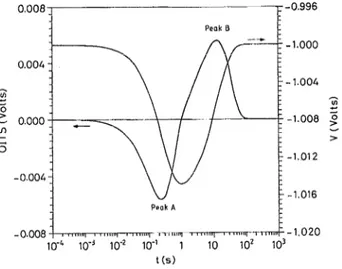
FIG. 1. Voltage transient and the OITS spectrum for as-grown GaAs (LEC) under 1.1 eV illumination at T = 80 K.
It can be shown that the OITS signal of an arbitrary tran- sient corresponds to a convolution product between the time constant distribution of the transient and the OITS signal of a purely exponential one.” In this case the OITS spectrum has a characteristic shape and it exhibits a max- imum located at:
tz7 .,ln,:) 3 (3)
-
with an amplitude given by K-l
OITS,,, =A ..&-K-w(K-l)l. (4)
In this way, the OITS technique allows us to determine for an optical transient its time constant distribution function. It is advantageous over the deep level optical spectroscopy (DLOS)21*22 because for this last technique the signal ob- tained for each photon energy corresponds to the contri- bution of all the levels with optical response. Then, to sep- arate each contribution it is necessary to carry out DLOS from different initial occupancy factor values. In addition, the application of this technique for complex systems- with nonexponential or multiexponential processes-may lead to misinterpretation of the experimental data. On-the other hand, the experimental implementation of the OITS method is easier than that of the multi-exponential analysis methods based on the Fourier transform23’24 or the method of moments.25 The experimental setup used has been re- ported elsewhere.26
RESULTS
Figure 1 shows the 1.1 eV optically induced transient and the corresponding OITS spectrum, obtained at con- stant capacitance from an LEC as-grown sample. The OITS spectrum has two peaks, one negative (labeled A) and the other positive (labeled B), of equal area corre- sponding to two exponential components of the transient. The B peak corresponds to the optical quenching associ-
0.15 0.00 z 2 > - 0.15 V cn I- i3 - 0.30 - 0.45 0. r 00’ Peak B , I I I I I 0.01 0.1 1 10 100 l( t (9 1
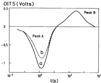
FIG. 2. GITS spectra under 1.1 eV illumination at T= 80 K for oxygen as-implanted samples: (a) dose 10” cm-‘, (b) dose 10” cm -‘.
ated with the EL2 level. Figure 2 shows the OITS spectra with an illumination energy of 1.1 eV from as-implanted 10” and 10” cm - 2 oxygen samples. The great increase of the quenching amplitude (B peak) from as-implanted ox- ygen samples compared to that from the as-grown one points out the creation of ELZrelated centers without a high-temperature annealing of the samples and corrobo- rates previous results reported by thermal and optical tech- niques in boron-implanted samples.‘9*27,28
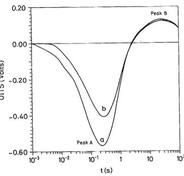
Unlike the as-grown samples, where the A and B peaks present the same areas,21 in the oxygen-implanted samples we observe a strong difference between both areas, being always the area of A peak greater than that of the B one. For the boron-implanted samples the spectra show a sim- ilar behavior, as can be observed in Fig. 3 (a), where we present the OITS spectra obtained from the 10” cm - 2 boron-implanted sample and annealed at 400 “C.
In the case of boron implantation, these differences have been partially explained taking into account the pre- viously proposed interaction mode127*28 between the EL2 defect and shallower levels created during the implantation processes, identified as the EL6 and EL5.‘9729 According to this model, the photoionization of these levels takes place through the EL2 one, previously ionized, which leads to an increase of the A peak amplitude in relation to that of the B one. This effect has been observed performing optical transients which these shallower levels previously emptied by thermal emission ( 180 K for 20 min) . The results (Figs. 3 and 4) show that only the area of the A peak decreases while the B peak remains unchanged. Nevertheless, only for photon energies equal or below 1.1 eV both A and B peaks have the same area.
The oxygen-implanted sampIes show a similar behav- ior. Previous results obtained by thermal transients in these samples also present defects with activation energies simi- lar to those of these shallower levels.29 The optical tran-
OITS (Volts)
I
FIG. 3. OITS spectra under 1.1 eV illumination at T= 80 K for the boron-implanted, 400 “C annealed sample: (a) first spectrum, (b) spec- trum after thermally emptying shallower levels (EL5, EL6) at 180 K for 20 min.
sients performed after emptying shallower levels, in the same experimental conditions than for the boron-im- planted samples (Fig. 5) show a decrease of the area of the A peak in relation to that of the B one. However, in this case the area of the A peak always remains greater than the B one for all illumination energies while the photoquench- ing effect is present.
To explain the remaining discrepancy between the A and B peak areas observed in both the oxygen- and boron- implanted samples after emptying the shallower levels two hypothesis can be assumed: (i) there are other deep levels with the same optical ionization rate of the EL2, perhaps EL2 defect without quenching (as has been proposed for the anion antisite defects produced in plastically deformed
OITS (Volts)
10-z 100 102
t(s)
FIG. 4. OITS spectra under 1.2 eV illumination at T = 80 K for the boron-implanted, 400 “C annealed sample: (a) tirst spectrum, (b) spec- trum after thermally emptying shallower levels (EL5, EL6) at 180 K for 20 min.
-1
Peak B-0.60 +---T--V-
10-3 lo-* 10-l 1 10 lo2 t (s)
FIG. 5. OITS spectra under 1.1 eV illumination at T = 85 K for the oxygen 10” cm _ 2 implanted, 450 ‘C annealed: (a) first spectrum, (b) spectrum after thermally emptying shallower levels (EL5, EL6) at 180 K for 20 min.
GaAs3’ or (ii) there is an optical recovery of the metasta- ble state that competes with the transfer from the stable state of EL2.-*14 In this case the area of the B peak ob- served will diminish. A third hypothesis, the presence of others levels nonemptied after the thermal emission during 20 min at 180 K which could also interact with the EL2, should be taken into account. However, the thermal ion- ization spectra (DLTS or ITS) from both oxygen- and boron-implanted samples only show a broad peak,
the
U band, in addition to the EL6 and EL5 ones. This band has been associated to an interaction between EL2 and shal- lower defects.31’32 Notice that the existence of a defect with thermal response in the U-band region may be masked by the signal from the U band, making its detection very dif- ficult. Anyway, its feasible existence does not modify the following analysis.To distinguish between the above hypothesis, a careful analysis of the experimental data is required. Since the optically generated carriers and/or the Debye tail carriers
m
-0.20\
l-
\
\
:
6
I, a I
’ ,’
- 0.40 A &10-3 10-Z 10-I 1 IO IO' IO3
t w
FIG. 6. OITS spectra under 1.1 eV illumination at T= 85 K for the oxygen as-implanted sample (dose 10” cm-‘). (a) Dashed line: lirst spectrum after cooling down, (b) solid line: next spectrum after a forward bias. pulse of 1000 s.
can produce an electrical regeneration process, which would be interpretated as an optical recovery,33 it is nec- essary to determine the electrical recovery process present in our samples.
From the measurements made at 80 K, we have ob- served that the ion-implanted samples do not show a com- pletely electrical recovery of the metastable state. Then, to assure the complete recovery of the EL2 metastable state after each illumination transient, the temperature was in- creased over 150 K. Table I presents the efficiency of the electrical recovery for implanted samples, obtained from the ratio between the quenching amplitude in the first op- tical transient after cooling down and the amplitude after a forward bias pulse 1000 s. This time should be enough to obtain the total recovery of the standard EL2 metastable state. This effect appears for both implanted specimens and increases with the implanted dose. Moreover, for the same implantation doses the electrical regeneration rate is greater for the boron-implanted samples. It should be noted that the 10” cm- 2 oxygen-implanted sample does not show electrical recovery (Fig. 6).
The failure of the electrical regeneration in oxygen- implanted samples has already been reported by Taniguchi and Ikoma,34 but in our case, we note that this effect is not
TABLE I. Efficiency of the electrical recovery for oxygen- and boron-implanted samples. The shallow defects concentration have been measured by thermal transients. For the 10” cm -’ oxygen as-implanted the shallow defect concentration has not been estimated, because the shallow levels peaks were overlapped by the U band.
Element Boron Boron Boron (Ref. 28) Oxygen Oxygen Oxygen Oxygen Dose (cm-*) 10” 10” 10” 1o’O 10’0 10” 10” Annealing temperature (“C) . . . 400 600 . . . 450 .*. 450 Electrical recovery (% ) 14 16.5 87 13 22 <l <l Shallow defect concentration (cm - s) 5.8 x 10’s 2.3 x lOI < lo’* 1.0 x 10’6 3.9 x lOI . . . 1.0 x 10”
0.4 '3i 0.2 5 > v 0.0 z cl -0.2 -0.4 10-3 10-t 10-l 1 IO IO2 IO3 t(s)
FIG. 7. OITS spectra for the oxygen as-implanted ( IO” cm - ‘) at T = 85 K under 1.1 eV illumination: (a) initial transient after illuminating 20 min with an excitation energy of: (b) 1, (c) 1.2, (d) 1.3, (e) 1.4 eV.
uniquely related to the oxygen samples, because it also appear in boron-implanted samples.
Once determined the inhibition factor of the electrical recovery process, a more accurate analysis of the pho- totransients has been performed in order to explain the discrepancy between the A and B peak amplitudes after emptying the shallower levels. The experimental sequence has been the following: First, the sample was cooled down to 85 K. Then it was illuminated with a reference energy hv = 1.1 eV during time tl = 25 min, long enough to reach the steady state. Afterwards, the illumination energy was changed to an excitation energy in the range 0.7 to 1.45 eV during a time t2 = 25 min. Finally the illumination was returned to hv = 1.1 eV and an OITS spectrum was re- corded. This process was repeated for different energies in this excitation range and the sequence has also been done for different reference energies. In all cases, as the optical transients were performed at constant capacitance condi- tions, the charge space region analyzed was fixed during the experimental process. In Fig. 7 we have plotted the spectra obtained from the as-implanted 10” oxygen ions/cm2 sample. These spectra can only be explained as- suming that the optical-induced transition between the me&table and the fundamental state takes place. The first peak in the spectra for the different excitation energies is due to a readjustment of the defect occupation factor cor- responding to the A peak, between
hv
= 1.1 eV and the excitation energy used. The second one is due to the quenching transition, carried out at reference energy 1.1 eV, of the EL2 recovered centers from the metastable state. Then, this quenching peak amplitude is a direct measure of the EL2 metastable optical recovery induced for the differ- ent excitation energies in relation to the quenching effi- ciency of the reference energy. This peak cannot be due to a population readjustment of other level, because in such a case it ought to appear also in the spectrum b of Fig. 6, where the EL2 was previously quenched usinghv =
1.1 eV. Moreover, it cannot be related to an electrical regen- eration process induced by the presence in the conduction0.50
0.00
-0.50
-1.00 I
10-3 10-Z 10-l IO0 IO' 102 IO3 t(s)
FIG. 8. OITS spectra for the 10” cm -’ boron-implanted and 400 “C! annealed sample at T = 80 K, under 1.1 eV illumination: (a) initial tran- sient after illuminating 20 min with an excitation energy of: (b) 1.15, (c) 1.2, (c) 1.25, (d) 1.3 eV.
band of optically generated carriers, or to an electrical re- generation induced by the free electrons in the Debye tail, because we have not observed any electrical regeneration in this sample.
Similar experiments have been performed for the bo- ron- and oxygen-implanted samples which show a partial electrical recovery process (Fig. 8). In Fig. 9 we have plotted the efficiency of the optical recovery versus the illumination energy for the different boron- and oxygen- implanted samples. This efficiency was calculated as the ratio between the quenching amplitude obtained for the reference energy before and after the illumination with ex-
,p lOOr---
0 .- 5 f aJ g so- v 2 5 .- “a0
B
s
o-
-
I
I
I
1.0 1.1 1.2 1.3 1.4 15hv (eV)
FIG. 9. Spectral dependence of the optical recovery ratio for different samples. $J: IO” cm -’ boron implanted, 400 “C annealed, X: 10”cm-’ oxygen as-implanted; 0: 10” cm- * oxygen implanted, 450 “C an- nealed, 0: IO” cm -’ oxygen as-implanted.
citation energies. We observe a similar evolution for all samples. This result points out that the optical recovery is found to be nearly independent on the boron or oxygen ion specimen nature and the annealing temperature below 500 “C. For reference energies equal to or below 1.1 eV the ’ optical recovery efficiency spectra are identical. It must be noted that for these energies, in boron-implanted samples, the A and B peaks have the same area after emptying the shallower levels. This result suggests that for these energies there is no optical recovery of the metastable state and as a consequence the optical recovery efficiency obtained is in- dependent of the reference energy. Moreover, as the optical recovery evolution is similar for boron and oxygen sam- ples, the differences observed in the areas of the A and B peaks from the OITS spectra in oxygen-implanted samples after emptying defects could be a possible manifestation of an oxygen-related defect with similar optical response to the EL2 or which can interact with the EL2 center. How- ever, the possibility of an optical recovery at energies equal or below 1.1 eV in the oxygen-implanted samples cannot be discarded.
DISCUSSION
The obtained results give direct evidence of the pres- ence of optical regeneration of the EL2 centers produced by oxygen and boron implantation. The spectral depen- dence of this optical recovery (Fig. 9) agrees qualitatively with the previous results reported by Parker and BrayI in oxygen-doped samples, which also observed a photoin- duced recovery process between 0.9 and 1.4 eV competitive with the usual photoquenching process. However, they ob- served a maximum of the spectral efficiency at 1.3 eV, and attributed the recovery process to the presence of oxygen modifying the EL2 defect.
Different authors4-6’14 have also reported examples of the photoinduced recovery process of the EL2 defect in SI GaAs samples in the optical range between 0.65 and 1.1 eV. Although in this case the recovery process is noncom- petitive with the photoquenching effect, only a partial re- covery (lo%-20%) is observed. More recently Manasreh and Fisher* have shown a new photoinduced recovery pro- cess by photon energies near the GaAs gap
(h-v>
1.4 eV) and with a high recovery ratio. Nevertheless, in all these cases the samples analyzed were as-grown and with a shal- low defect concentration very much lower than in our sam- pleS.Unlike these previous results, in our samples the ob- served electrical and optical recovery processes seem to be related to the implantation damage and the feasible defect interaction. The electrically active shallow defect concen- trations shown in Table I are an indication of total defect concentration which is related to the annealing tempera- ture and implantation dose. Both the photoionization am- plitude transient of the stable state of EL227 (peak A in Fig. 2) and the electrical recovery ratio of the metastable state (Table I) strongly depend on the created defects. These seem to indicate that the lattice damage induced by the implantation process modifies the properties of the EL2
defect. In the following, we are going to .analyze the rela- tionship between the electrical and optical recovery and the implanted damage.
A lirst possible explanation of the electrical recovery failure may be based on a diminution of the carriers on the conduction band caused by a compensation process. It is well known that both boron and oxygen implantation can produce a semi-insulating layer in previously n-doped GaAs,35 which is usually applied to obtain planar device isolation in GaAs integrated circuits.
However, from the measurement of the free carriers profile, we have deduced that the complete electrical re- covery of the centers ought to take place in less than 1 ms, and this has not been observed even for forward bias times of the order of hundreds of seconds. Moreover, when the samples are cooled down from room temperature to 80 K at forward bias and under illumination, the following OITS spectrum, obtained by switching the sample to reverse bias, does not show any photoquenching signal. This fact indi- cates that it is possible to induce the quenching process even in the semiconductor neutral zone, which is in agree- ment with the observed inhibition of the electrical recovery process of the quenching state. These data suggest a mi- croscopic origin for the inhibition effects on the electrical recovery process.
Nevertheless, another explanation that assumes that the damage produced by the ion bombardment modifies locally the free carrier concentration is possible. Under these conditions, Makram-Ebeid and Boher36 proposed the existence of damage clusters, with a large number of densely packed defects. Across this damaged region, the energy band diagram is modified and the Fermi level is strongly pinned at midgap defects. Then, when we apply a forward bias pulse to reduce the diode depleted region, cluster regions will remain empty of free carriers. If the EL2 defect observed were located in these clusters the cap- ture processes would be slowed by the lower carrier con- centration. However, we have observed that in the dark- ness at 80 K, the EL2 defect presents the normal value of its electron capture cross section.
As a consequence, the failure of the electrical recovery process must be due to the existence of an interaction be- tween the basic EL2 defect and others defects created dur- ing the implantation process. The higher inhibition on the electrical recovery process in the oxygen-implanted sam- ples in relation to the boron-implanted ones would be re- lated to the higher damage induced by the heavier im- planted ion. This explanation has been corroborated by measurements carried out in annealed implanted samples, which show an increase of the electrical recovery when shallow defects created by implantation vanish.‘ss29
However, for the photoinduced recovery process in the l-l.4 eV range, we have observed a very weak dependence with the shallower levels concentration (Fig. 9). This pro- cess has been observed in the same spectral range by other authors in samples as-grown and oxygen doped, and in other optical ranges in LEC and semi-insulating GaAs. In these samples, the concentration of shallower defects is not significant. Then, we can argue that the photoinduced re-
covery process has a different origin than the failure of the electrical recovery, more likely related to the microscopic structure of EL2 metastable state.
Taking into account these considerations, as well as the similarities in the photorecovery response in oxygen- doped and boron- and oxygen-implanted samples, we think that the changes induced in the basic EL2 defect are sim- ilar. It is then necessary to analyze the possible resem- blance among the EL2, the oxygen-related defects, and the deep defects produced by implantation.
good description of the electrical recovery mechanism but does not give information about the photoinduced recovery from metastable EL2. To explain this process observed at energies between 1.4 and 1.5 eV, Manasreh and Fisher8 proposed the Asoa - VAs model. Finally, an extensive dis- cussion about the presence of arsenic and gallium vacant defects in the microscopical structure of EL2 family and their influences in the optical and electrical characteristics has been reported by Wager and Van Vetchen.42*4’
In fact, the microscopic structure of the oxygen-related centers in GaAs is also not completely known. Absorption measurements have allowed the identification of two bands associated to the isolated oxygen interstitial defect, Of, and . a complex defect of arsenic vacancy and oxygen labeled Ga-0-Ga defect.37X38 Recently, many works have been de- voted to analyze the electrical behavior of these defects. The interstitial oxygen is a nonelectrically active defect, however; Bourgoin et aZ.39 have suggested that the Oi in- teracts with the EL2, changing its DLTS spectrum at tem- peratures higher than 300 K.
In contrast to the previous results where an oxygen- related defect labeled EL0 shows an activation energy for electron emission similar to the EL2,40 Neild, Skowronski, and Lasows4t have identified a DLTS peak located at 0.55 eV below the conduction band as due to the Ga-0-Ga defect. In both cases, the models proposed for the oxygen- related deep leve141’42 assume a complex defect formed by an oxygen atom in the site of arsenic and arsenic and/or gallium vacancies.
From our results, and according to the above consid- erations, we propose that the existence of an EL2 photo- induced recovery process in semi-insulating, oxygen-doped and boron- and oxygen-implanted samples could be related basically to the interaction between the basic EL2 (Asoa antisite) and an arsenic vacancy defect and/or gallium va- cancy. The implantation process can assist the complex defect creation from this simple defect, and that would explain the changes in the metastable optical recovery ob- served. The similar vacancy distribution for the oxygen- and boron-implanted samples could explain the similar op- tical recovery spectral dependence. Assuming this hypoth- esis, for the oxygen-doped samples, this atom would in- crease the vacancy defect concentration and help its interaction with the Asoa defect. Nevertheless, more exper- iments will be necessary to determine an accurate micro- scopic model.
CONCLUSIONS
In a similar way, we should also consider the defects related to the boron atom. Unlike the oxygen atom, which presents an electrically active deep level, previous works have only reported for the boron a shallow double acceptor
BAS 43 Only for implanted boron samples at high doses
> 10’3cm-3 and annealed at
T
> 500 0C,44 the existence of boron-related complex defects has been suggested.In consequence, it seems necessary to consider the deep defects due to the ion implantation process, to find the similarity between oxygen and boron effects. In both cases, a significant modification of the lattice order is produced. Many atoms are displaced of their sites and may be placed at interstitial positions. By the assumed microscopic mod- els of EL2, some displaced arsenic atoms will make AsGa antisite defects and will be the basis of the created EL2. In the neighborhood of these created defects the crystal net- work is very perturbed and there exists structural defects such as arsenic and gallium vacancies and interstitial at- oms, which can interact, forming complex defects.
In summary, we have analyzed the voltage phototrans- ients obtained at constant capacitance conditions from bo- ron- and oxygen-implanted samples using optical isother- mal transient spectroscopy. The results point out that the ion implantation process creates EL2-like defects, which interact with shallower levels also produced by the implan- tation. The created EL2 presents a partial or complete in- hibition of the electrical recovery. This behavior does not depend on the implanted specimen (boron or oxygen) and is clearly related to the presence of damage defects. We have also determined the existence of an optical induced recovery process from the metastable state competing with the photoquenching effect in the spectral range 1.1-1.4 eV. The spectral dependence of this optical recovery has been found to be basically independent of the ion specimen, dose, and annealing for temperatures below 450 “C. Fi- nally, a model is suggested for the EL2 defect which pre- sents optical recovery consisting of a complex that involves AsGa and gallium and/or arsenic vacancies.
Since the optical recovery process is also observed, without noticeable modifications, in the annealed samples
(T~45.0
“C), it is not probable that the interstitial atomswould be the origin of this process because they present a high mobility at relatively low temperatures. Therefore, it seems that the vacancies may account for the behavior found. A possible relation between the EL2 and the vacant defects has been previously reported: by theoretical consid- erations some models propose that the metastable state of the EL2 is the Asi - Voa split.“-I3 This model provides a
’ G. M. Martin and S. Makram-Ebeid, Deep Centers in Semiconductors,
edited by S. T. Pantelides (Gordon and Breach, New York, 1986), p.
399.
‘J. C. Bourgoin, H. J. Bardeleben, and D. Stievenard, J. Appl. Phys. 64, R65 (1988).
“G. Guillot, Rev. Phys. Appl. 23, 833 (1988).
4Y. Mochizuki and T. Ikoma, Jpn. J. Appl. Phys. 24, L895 ( 1985). ‘S. Nojima, J. Appl. Phys. 58, 3485 (1985).
6D. W. Fisher, Appl. Phys. Lett. 50, 175 (1987).
‘M. Tajima, H. Sauto, T. Imo, and K. Ishid, Jpn. I. Appl. Phys. 27,410l
t 1988).
aM. 0. Manasreh and D. W. Fisher, Phys. Rev. B 40, 11756 (1989). ‘H. J. von Bardeleben, D. Stievenard, D. Dereames, A. Huber, and J. C.
Bourgoin, Phys. Rev. B 34, 7192 (1986).
i”B. K. Meyer, D. M. Hofman, J. R. Niklas, and J. M. Spaeth. Phys. Rev. B 36, 1332 (1987).
I’M. Kaminska, M. Skowronski, and W. Kuszks, Phys. Rev. Lett. 55,204
(1985).
i2D. J. Chadi and K. J. Chang, Phys. Rev. Lett. 60, 2187 (1988). 13J. Dabrowski and M Scheffer, Phys. Rev. Lett. 60, 2183 (1988). “J. C. Parker and R. Bray, Phys. Rev. B 37, 6368 (1988).
“U. V. Desnika, D. I. Desnika, and B. Santic, Appl. Phys. Lett. 58, 278 (1991).
t6T. R. Jervis, D. W. Woodard, and L. F. Eastman, Electron. Lett. 16, 621 (1976).
“M. Taniguchi and T. Ikoma, Inst. Phys. Conf. Ser. 65, 65 (1983). ‘*G. M. Martin, P. Terriac, S. Makram-Ebeid, G. Guillot, and M. Ga-
vand, Appl. Phys. Lett. 42, 61 (1983).
I9 J. R. Morante, A. Perez, J. Samitier, and A. Romano. J. Appl. Phys. 70,
4202 (1991).
z”J. Samitier, J. R. Morante, A. Cornet, A. Herms, P. Roura, and A. P6rez, Mater. Sci. For. 10-12, 539 (1986).
2’A. Chantre, G. Vincent, and D. Bois, Phys. Rev. B 28, 5335 (1981). 22G. Vincent, D. Bois, and A. Chantre, J. Appl. Phys. 53, 3643 (1982). ‘,S. W. Provenchar, Compt. Phys. Commun. 27, 213 (1982).
24K. Ikeda and H. Takaoka, J. Appl. Phys. 54, 6031 ( 1983).
“I. Isenberg, R. D. Dyson, and R. Hanson, Biophys. J. 13, 1090 ( 1973). 26S Marco, J. Samitier, J. M. Mpez-Villegas, and J. R. Morante, Meas.
Sci. and Tech. 2, 899 (1991).
“J. Samitier, J. R. Morante, L. Giiaudet, and S. Gourrier. Appl. Phys. Lett. 48, 1138 (1986).
‘s-4. Pbrez, J. Samitier, J. Esteve-Tinto, A. Romano, and J. R. Morante, Defect and Diffusion Forum 62/63, 77 (1989).
s9S. Marco, J. Samitier, J. R. Moran& P. Boher, and M. Renaud, in
Proceedings of the 6th International Conference on Semi-Insulating III-
V Materials, Toronto 1990, edited by A. G. Milnes and C. Miner (Adam Hilger, Bristol, 1990).
“D. M. Hofman, B. K. Meyer, J. M. Spaeth, M. Wattenbach, J. Kriiger, C Kisielowski-Kemmerich, and H. Alexander, J. Appl. Phys. 68, 3381 (1990).
32J. R. Morante, J. Samitier, A. Perez, H. Altelarrea, and S. Gourrier, J. 31G. M. Martin, E. E&eve, P. Langlade, and S. Makram-Ebeid, J. Appl.
Appl. Phys. 60, 1661 (1986).
33X. Boddaert, D. Stievenard, and J. C. Bourgoin, Phys. Rev. B 40, 1051 Phys. 56, 2655 (1984).
(1989).
34M. Taniguchi, T. Ikoma, Proc. 2nd Conf. Semi-Insulating III-V Mate- rials, Evian, 1982, edited by S. Makram-Ebeid and B. Tuck, p. 283. 3sJ. Samitier, J. R. Morante, A. Miralles, A. Cornet, A. Herms, and S.
Gourrier, Proc. 4th Conf. ou Semi-Insulating III-V Materials, Hakone 1986, p. 579.
36S. Makram-Ebeid and P. Boher, Rev. Phys. Appl. 23, 847 (1988). 37X. Zhong, D. Jiang, W. Ge, and C. Song, Appl. Phys. Lett. 52, 628
(1988).
38J. Schneider, B. Dischler, H. Seelewind, P. M. Mooney, J. Lagowski, M. Matsuni, D. R. Beard, and R. C. Newman, Appl. Phys. Lett. 54, 1442
(1989).
“J. C. Bourgoin, D. Stievenard, D. Deresmes, and J. Mimila-Arroyo, J. Appl. Phys. 69, 284 (1991).
4oJ. Lagowski, D. G. Lin, T. Aoyama, and H. C. Gatos, Appl. Phys. Lett.
44, 336 (1984).
41 S T. Neild, M. Skowronski, and J. Lagowski. Appl. Phys. Lett. 58, 859 (1991).
“J. F. Wager and J. A. Van Vetchen, J. Appl. Phys. 62, 4192 (1987). 43P. Dansas, J. Appl. Phys. 58, 2212 (1985).
“G. M. Martin, P. Secordel, and C. Verger, J. Appl. Phys. 53, 8706 (1982).
4s J. F. Wager and J. A. Van Vetchen, Phys. Rev. B 35, 2330 ( 1987).