DEPARTAMENT DE FÍSICA APLICADA I ÒPTICA
Martí i Franquès 1, 08028 Barcelona
AMORPHOUS SILICON SOLAR CELLS OBTAINED BY HOT-WIRE
CHEMICAL VAPOUR DEPOSITION
David Soler i Vilamitjana
Memòria presentada per optar al grau de Doctor Barcelona, setembre de 2004
DEPARTAMENT DE FÍSICA APLICADA I ÒPTICA
Martí i Franquès 1, 08028 Barcelona
AMORPHOUS SILICON SOLAR CELLS OBTAINED BY HOT-WIRE
CHEMICAL VAPOUR DEPOSITION
David Soler i Vilamitjana
Programa de doctorat: Tècniques Instrumentals de la Física i la Ciència de Materials Bienni: 1998-2000
Tutor: Enric Bertran Serra Director: Jordi Andreu Batallé
Memòria presentada per optar al grau de Doctor Barcelona, setembre de 2004
This work has been carried out in the Photovoltaic Group of the Laboratory of Thin Film Materials of the Department of Applied Physics and Optics of the University of Barcelona. The Photovoltaic Group is a member of the Centre de Referència en Materials Avançats per a l’Energia de la Generalitat de Catalunya (CeRMAE). The presented work has been supervised by Dr. Jordi Andreu Batallé in the framework of the projects TIC98-0381-C02-01 and MAT2001-3541-C03-01 of the CICYT of the Spanish Government and with the aid of the project ENK5-CT2001-00552 of the European Commission, and supported by a pre-doctoral grant from the Spanish Government (Beca FPI).
Contents
Agraïments ...3
Outline of this thesis ...5
1. Introduction ...7
1.1. Thin film technologies for photovoltaic applications...7
1.2. Hydrogenated amorphous silicon as a photovoltaic material...9
1.3. Hot-Wire Chemical Vapour Deposition ...11
1.4. Thin film silicon solar cells technology ...14
1.5. a-Si:H at Universitat de Barcelona ...17
1.6. Aim of this work...18
2. The Hot-Wire CVD reactor. Characterization techniques...19
2.1. The Hot-Wire CVD reactor ...19
2.2. Characterization techniques...23
2.2.1. Structural characterization ...23
2.2.2. Electrical characterization...25
2.2.3. Optical characterization ...28
2.3. Device characterization ...30
3. a-Si:H to nc-Si:H transition...37
3.1. a-Si:H on the onset of microcrystallinity...37
3.2. Influence of filament temperature ...38
3.3. Influence of pressure...46
3.4. Influence of hydrogen dilution ...49
3.5. Influence of substrate temperature...52
3.6. Summary...55
4. Intrinsic a-Si:H by Hot-Wire CVD ...57
4.1. Device-quality intrinsic amorphous silicon...57
4.2. Our intrinsic amorphous silicon ...59
4.2.1. Structural properties...59
4.2.2. Electrical properties ...66
4.2.3. Optical properties...71
4.3. Deposition conditions ...74
4.3.1. Influence of filament temperature...74
4.3.2. Influence of pressure...76
4.3.3. Influence of hydrogen dilution ...81
4.4. Summary...84
5. Hot-Wire deposited doped material...87
5.1. Introduction...87
5.2. n-type material ...88
5.3. p-type material ...91
Contents
5.3.2. p-type nc-Si:H...99
5.3.3. p-type a-Si:H vs. p-type nc-Si:H ... 101
5.4. Substrate influence ... 102
5.4.1. Structural properties ... 103
5.4.2. Electrical properties... 104
5.5. Summary... 108
6. Amorphous silicon solar cells... 111
6.1.Introduction ... 111
6.2. p-type a-Si:H front contact ... 112
6.3. p-type nc-Si:H front contact ... 122
6.4. p-type double structure: nc-Si:H/a-Si:H front contact ... 124
6.5. Back reflector ... 128
6.6. Our final sep ... 131
6.7. Device stability... 135
6.8. Summary... 139
7. Solar cell simulation... 141
7.1. p-i-n solar cell operation... 141
7.2. Numerical analysis ... 146
7.2.1. Optical absorption... 146
7.2.2. DICE technique ... 148
7.2.3. Numerical resolution of the equations... 152
7.3. Summary... 159
Conclusions ... 161
Annexe: Additional applications... 165
A.1.Silicon based thin film transistors ... 165
A.1.1. Introduction... 165
A.1.2. Experimental... 167
A.1.3. Results... 168
A.2. Heterojunction solar cells ... 169
A.2.1. Introduction... 169 A.2.2. Experimental... 171 A.2.3. Results... 172 References ... 175 Acronym list... 187 Figure list ... 189 Table list ... 195 Resum en català... 197
Agraïments
El treball que es presenta en aquesta tesi constitueix el resultat de més de cinc anys de recerca. Durant aquest llarg període han estat moltes les persones que de manera més o menys directa han contribuït a que aquest escrit veiés finalment la llum.
En primer lloc voldria mostrar el meu agraïment al Dr. José Luís Morenza, director del Departament de Física Aplicada i Òptica durant el període de realització d’aquesta tesi, per acceptar-me com a estudiant de doctorat oferint-me d’aquesta manera la possibilitat d’introduir-me en el món de la recerca.
Seguidament voldria agrair al Dr. Jordi Andreu, director d’aquesta tesi i cap del Grup Fotovoltaic, pel seu important suport durant la realització d’aquesta tesi. També voldria expressar el meu agraïment al Dr. Joan Bertomeu, especialment pels seus savis consells al laboratori. Per altra banda, voldria agrair molt especialment la seva col·laboració al Dr. José Miguel Asensi per les interessants discussions i el seu tracte sempre amable i atent, així com la seva disposició a resoldre sempre alguns dels meus infinits dubtes.
També voldria agrair el seu ajut al Dr. David Peiró, qui durant els primers mesos de realització d’aquesta tesi em va explicar el funcionament del reactor de Hot-Wire CVD, així com d’algunes de les tècniques de caracterització, sense perdre mai el bon humor. Mereix un capítol a part el Dr. Cristóbal Voz, font d’inspiració al llarg d’aquests anys i un autèntic exemple a seguir. La seva generositat a l’hora d’explicar els seus abastos coneixements, la seva paciència infinita i el seu tracte sempre amable han fet d’ell un autèntic pilar en la realització d’aquesta tesi. A més, també voldria agrair-li les moltes converses i els bons moments conviscuts.
Han estat més de cinc anys compartits amb la Dra. Marta Fonrodona. De fet, encara recordo el dia que vam començar plegats la llarga (per a uns més que per a altres, jeje) travessa del doctorat. Fent balanç ara que això s’acaba veig que han estat infinites hores de laboratori, discussions, correccions (gràcies per tenir la paciència de llegir la tesi).... Bé, l’únic que puc dir és que t’agraeixo el suport i (encara més) l’amistat que m’has donat durant tots aquests anys (i les entrades al Camp Nou!, ei que és broma). Gràcies Marta! Voldria agrair també el seu suport i ànim a Jordi Escarré i a Ferran Villar, els quals han col·laborat, especialment en la sovint desagraïda feina de laboratori, a la finalització d’aquesta tesi durant aquests últims anys. A més, al Ferran voldria agrair-li el seu interès pel desenvolupament d’aquesta tesi i la seva “entranyabilitat” (era així, no?). Per altra banda, al Jordi voldria agrair-li molt sincerament la seva amistat i les moltes bones estones conviscudes (encara pateixo per les claus del cotxe). També voldria agrair molt especialment a Delfina Muñoz, companya de feina durant aquest últim any, per la seva vitalitat, optimisme i per la seva eficiència que tant m’ha ajudat per finalitzar la tesi.
També vull donar les gràcies al Dr. Juan Marcos Fernández i al Dr. Pere Serra, amb qui he compartit molt bones estones i a qui he d’agrair el seu ajut des dels primers dies al Departament. Al Marcos voldria agrair-li els infinits consells (ai, el Corel...) i les classes de guitarra gratuïtes. Al Pere li agraeixo les llargues converses i, molt especialment, les seves
Agraïments
recomanacions (gairebé) sempre encertades en temes de literatura o cinema.
Trigar més de cinc anys al Departament m’ha permès conèixer un gran nombre de persones que m’han inspirat i amb qui he compartit experiències. No se si sense tot aquest grup de persones la tesi també s’hauria dut a terme, però del que estic segur és que, en tot cas, hauria estat una tasca força més feixuga. Així, voldria expressar el meu sincer agraïment a l’Ángel (un home seriós, o no tant?), l’Albert (gràcies per la xocolata txato), el Jordi i la Cristina (la parella que “vino de la Tierra Media” amb el seu bon rotllo), el Carles (has vist la peli...?), la Maryory i el William (gràcies paisas), el Céspedes (sempre amb un acudit a punt, 2+3?), la Maria (gràcies per l’alegria que ens has portat des de Men...Mallorca, ui. Trobarem un altre nanosounds?), el Xavi (sempre elegant) i el Marc (sempre amb un somriure a punt. Pots tornar a tocar el “Nothing Else Matters”?).
Voldria mostrar el meu agraïment al company Jordi Solà, sense la seva eficiència és molt probable que jo encara estigués intentant inscriure la tesi. També vull donar les gràcies a Francisco Romero pel seu ajut a l’hora de resoldre tant problemes informàtics (tan comuns...) com avaries als diferents sistemes del laboratori (ai, l’evaporadora...).
També voldria expressar el meu agraïment al Dr. Jaime López i al Dr. Pere Lluís Miribel pels seus savis consells i per l’interès que han mostrat en tot moment per aquest treball. Des del moment de començar aquesta tesi, ha estat agradable (i necessari) tenir companys de quinta amb qui compartir experiències. Així, voldria agrair a l’Enric, el Toni, la Laura i el Raúl per totes les vivències i consells compartits. Per cert, no cal dir qui ha estat l’últim de la colla en acabar la tesi, no?
Mirant enrera, és agradable recordar alguns dels companys de carrera amb els quals hem compartit les millors estones. Així, voldria agrair molt especialment al Jesús, el Sergi, el Puxeu, el Javi, el Ferran i el David (la primera persona amb qui vaig parlar fa uns deu anys quan vaig posar els peus a la Facultat).
Si hi ha alguna persona que m’ha donat l’últim empenta per a que aquesta tesi es materialitzés, aquesta ha estat la Mònica, amiga, companya i autèntica font d’energia durant aquests últims mesos de tesi. A mida que la cursa de la tesi s’acosta al seu final, és curiós com aquest sembla allunyar-se. Gràcies per haver tingut la confiança i el convenciment (sovint més que jo) de què algun dia arribaria a la línia d’arribada. També voldria agrair a tota la gent de “Sugranyes”, especialment al Manuel, pel bon ambient i la seva alegria, sempre tant necessària a l’hora de “desconnectar” de la tesi.
També vull agrair tots els membres del tribunal d’aquesta tesi per acceptar formar part del mateix i, sobretot, per llegir aquest escrit.
Finalment, voldria agrair la infinita paciència i comprensió dels meus pares, sense el vostre suport aquesta tesi no hauria arribat mai a port.
El més probable és que m’hagi deixat algú en aquesta llista d’agraïments. Si és així, cap problema, feu-m’ho saber i us tindré en compte per a la propera tesi. Ara que, ben mirat, potser amb aquesta ja n’hi ha prou, no?
Outline of this thesis
This thesis is focused on the deposition of hydrogenated amorphous silicon (a-Si:H) based photovoltaic devices by means of Hot Wire Chemical Vapour Deposition (Hot-Wire CVD). Hot-Wire CVD allows the growth of device quality a-Si:H at relatively low substrate temperatures, thus allowing the use of low-cost substrates, whereas keeping acceptable high deposition rates. Additionally, reasonably low implementation and upkeep costs are associated to this technique, thus making Hot-Wire CVD a very attractive alternative for industrial application. This work concerns both the material properties (structural, electrical and optical) and the photovoltaic performance of preliminary obtained solar cells. An overview on the contents of each chapter is described below.
Chapter 1. Introduction
In this chapter, a general introduction to thin film technologies for photovoltaic applications is given. Hydrogenated amorphous silicon (a-Si:H) properties are described and Hot-Wire Chemical Vapour Deposition (Hot-Wire CVD) is presented as a viable technique for its deposition. Finally, an overview of the previous works concerning a-Si:H carried out at Universitat de Barcelona is given.
Chapter 2. The Hot-Wire CVD reactor. Characterization Techniques
This chapter describes both the Hot-Wire CVD reactor at Universitat de Barcelona and the experimental techniques used to analyse structural, optical and electrical properties of the deposited layers. Additionally, techniques involved in the characterization of photovoltaic devices are also described.
Chapter 3. a-Si:H to nc-Si:H transition
In this chapter, the influence of the deposition conditions on the material crystallinity, and consequently on its optoelectronic properties, is analysed. The transition from a-Si:H to nc-Si:H is studied after variations on either the filament temperature, pressure, hydrogen dilution or substrate temperature.
Outline of this Thesis
Chapter 4. Intrinsic a-Si:H by Hot-Wire CVD
In this chapter, the required properties of a-Si:H layers for application in solar cells are presented. The influence of the deposition conditions on the material quality is studied and our state-of-the-art material is presented. Moreover, low substrates temperatures (below 200ºC) are employed throughout the study to consider the future use of low-cost substrates.
Chapter 5. Hot-Wire deposited doped material
In this chapter we study optoelectronic features of both n-type and p-type thin silicon films. Special attention is paid to the deposition of p-type material due to the specific difficulties associated to its production. In that sense, both p-type a-Si:H and nc-Si:H are analysed and special treatments described. Finally, the photovoltaic suitability of the deposited material is examined.
Chapter 6. Amorphous silicon solar cells
In the present chapter, the performance of different photovoltaic devices is analysed. Preliminary results of p-i-n structures deposited onto textured substrates (Asahi-U) is presented. Further on, the effect of different strategies, especially those aiming to improve the front contact properties and the optical absorption (light trapping), are evaluated.
Chapter 7. Solar cell simulation
In this chapter, the fundamental performance of solar cells is described both in the ideal and in the realistic case. Moreover, simulation results bringing some additional light into the device physics are presented. These simulations are employed to analyse experimentally obtained results.
1. Introduction
In this chapter, a general background to thin film technologies for photovoltaic applications is given. Hydrogenated amorphous silicon is presented as a suitable material for application in solar cells and Hot-Wire Chemical Vapour Deposition is introduced as a viable technique for its deposition. Finally, a general retrospective regarding previous works carried out at Universitat de Barcelona concerning amorphous silicon is presented.
1.1. Thin film technologies for photovoltaic applications
Different semiconducting materials with suitable optoelectronic properties have been proposed for photovoltaic applications. Among these, silicon has been the most widely accepted one over the last decades. Not only does silicon fulfils the physical requirements for application in solar cells, but it is also abundant in nature and can be processed at relatively low costs, thus leading to a lowering on the energy Pay-Back time, i.e., the time needed for a photovoltaic system to produce electrical energy until it pays back the energy costs associated with its production.
Monocrystalline silicon (c-Si) based is the most established technology in photovoltaic industry. c-Si solar cells have been commercially available for years and satisfactory performances have been achieved. Thus, conversion efficiencies (η) around 25% in laboratory cells and 23% in commercial modules [Green et al. 2004] have been reported. Anyhow, some drawbacks arise from the use of c-Si, concerning mainly the production costs associated to the techniques involved in the growth of high-purity bulk silicon, which require much energy. Multicrystalline silicon (mc-Si) based solar cells have been developed as a lower cost alternative. In this technique, liquid silicon is solidified, leading to crystal structures of varying sizes at whose borders defects emerge. As a consequence, lower η values (around 20% for laboratory cells and 15% for commercial modules [Green et al. 2004]) are achieved when compared with c-Si technology.
Results obtained with both c-Si and mc-Si have led them to account for around 85% of the total photovoltaic panels market. Nevertheless, a further reduction in production costs is
1. Introduction
still desirable, and it is at this point that thin film technologies emerge as a highly promising alternative. Not only production costs are lowered, but some other important advantages arise from thin film technologies: low amount of material required, deposition over large area substrates or ease of mass production. Moreover, contrary to bulk-based technologies, where the silicon wafer itself works as a substrate, glass or another substrate material (stainless steel, polymer) is used to deposit thin film materials. Hence, thin film devices are especially suitable for a large number of applications, particularly those involving the use of light and flexible substrates. Among thin film materials, hydrogenated amorphous silicon (a-Si:H) has led to one of the most mature photovoltaic technologies, as it has been used over the last 25 years. Initial η around 9-10% have been reached in the laboratory for single junction cells, whereas values up to 13% have been achieved by means of multiple structures (tandem or triple-junction) involving silicon alloys (mainly with Ge) [Guha et al. 2000]. On the other hand, conversion efficiencies around 10% have been obtained when dealing with commercial modules based on triple-junction structures [Green et al. 2004], whereas moderate values around 5-6% have been reached when single junction a-Si:H modules are considered. In spite of the lower efficiencies achieved with a-Si:H when compared with c-Si (and mc-Si), the potential of a-Si:H to reduce production costs seems to lead to a gradual replacement of the most established bulk crystalline silicon technology.
Despite the encouraging results obtained with a-Si:H, some drawbacks (presented below) have led to the study of a variety of additional thin film technologies for photovoltaic applications. On one hand, alternative thin film silicon-based materials have been proposed. Hence, polycrystalline silicon (poly-Si:H) [Iiduka et al. 1997, Schropp and Zeman 1998], microcrystalline silicon (µc-Si:H) [Shah et al. 2003] or nanocrystalline silicon (nc-Si:H) [Hazra and Ray 1999, Brühne et al. 2001], all of them consisting of a mixture of both amorphous and crystalline material, have received much attention. On the other hand, different materials such as Copper Indium Diselenide (CuInSe2) [Mickelsen
and Chen 1980, Nakada et al. 1997], Cadmium Telluride (CdTe) [Fulop et al. 1982, Hanafusa et al. 2001] or Gallium Arsenide (GaAs) [Henini 2000, Yamaguchi 2003] have also been introduced into photovoltaic research. Although these materials result in solar cells with satisfactory performances, the use of toxic elements and/or the lack of availability of some of them, limit their global application. Finally, organic materials have
also been recently proposed [Waldauf et al. 2004]. Nevertheless, low conversion efficiencies and poor stability are still observed, although SIEMENS researchers have recently announced an increase of the efficiency of organic solar cells from the commonly obtained value of 3% to over 5%. In summary, and despite the recent progress obtained with alternative materials, around 90% of the total thin film solar cells production is still based on silicon technologies.
1.2. Hydrogenated amorphous silicon as a photovoltaic material
Hydrogenated amorphous silicon (a-Si:H) has become one of the most studied photovoltaic materials since its promising optoelectronic properties were first demonstrated. First studies regarding amorphous silicon (a-Si) revealed a high density of dangling bonds in the material. These dangling bonds act as defect states, thus leading to the presence of recombination centres and traps, which limit the electrical properties of the material and impede its use in photovoltaic applications. Passivation of dangling bonds is therefore necessary to improve the electrical features of the material. In that sense, dangling bonds can be passivated by the addition of hydrogen during the deposition process, thus leading to the well-known a-Si:H, whose electrical properties permit its use in solar cell technology [Pankove and Carlson 1977, Street 1991]. In particular, [Chittick et al. 1969] showed that a-Si:H could be obtained by Plasma Enhanced Chemical Vapour Deposition (PECVD) with better properties than those achieved with traditional techniques (evaporation and sputtering), making it suitable for optoelectronic applications. Furthermore, a-Si:H technology experienced an increasing interest after Spear and LeComber reported on the substitutional doping of a-Si:H by adding small amounts of either diborane (p-type doping) or phosphine (n-type) in 1975 [Spear and LeComber 1975]. As far as a-Si:H photovoltaic research is concerned, first solar cells with efficiencies around 2-3% were obtained by Carlson and Wronski [Carlson and Wronski 1976].
Contrary to monocrystalline silicon (c-Si), the absence of long-range order in a-Si:H causes a relaxation in the transition rules, so that it behaves as a direct gap semiconductor with a band gap between 1.6 and 1.8 eV. This behaviour results in a much larger absorption in the solar spectrum range, so much less material is needed to collect the same amount of incoming light. Hence, active (intrinsic) layer thicknesses below 0.5 µm are
1. Introduction
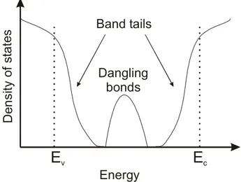
commonly used in a-Si:H solar cells, whereas much thicker layers (around 200 µm) are required for crystalline silicon ones. Regarding the above mentioned gap, it must be taken into account that this term can not be understood in the same way as when dealing with c-Si, where no electronic states can be found between the valence and conduction bands. A significant density of electronic states, which limit the mobility of photogenerated carriers, can be observed in a-Si:H in the so-called band gap, thus giving place to the commonly used expression mobility gap instead of band gap. Two different mechanisms account for the presence of electronic states in the mobility gap. On one hand, the lack of order in the material causes a broadening of the valence and conduction bands leading to band tails, where localized energy states exist. On the other hand, unpassivated dangling bonds give rise to defect states near the centre of the band gap as also seen in a-Si [Street 1991]. A schematic diagram of the a-Si:H density of states (DOS) can be observed in Figure 1.1.
Energy D en si ty o f st a te s
E
cE
v Band tails Dangling bondsFigure 1.1.. Schematic representation of the density of states (DOS) in a-Si:H.
The above-mentioned density of states in the band gap results in the low mobility of the carriers in a-Si:H due to significant recombination probability. As a result, drift current drives thin film solar cells as will be presented in section 1.4, whereas the performance of bulk solar cells relies on diffusion current [Green 1992]. Drift current requires an intense internal electric field, so that carriers photogenerated in the intrinsic layer can be effectively collected. Unfortunately, this electric field is also degraded by the defect states in the centre of the mobility gap, thus influencing the device performance.
A very critical phenomenon has been related to a-Si:H since first studies were reported: the Staebler-Wronski effect [Staebler and Wronski 1977]. This effects consists in the worsening of the material properties after prolonged light exposure due to the creation of metastable defects. Such defects act as recombination centres and degrade the internal electric field, so that collection is hindered and drift current is therefore reduced. The microscopic mechanism behind this degradation has not been fully clarified yet, though different models have been proposed over the years [Kamei et al. 1996, Branz 1998, Stradins 2003]. Anyway, hydrogen has been accepted to play a very important role, as high hydrogen content promotes the degradation of the samples. Hence, samples exhibiting low hydrogen content experience weaker degradation after light exposure [Mahan et al. 1991]. On the other hand, the use of thinner intrinsic layers in solar cells leads to lower collection distances and more intense electric fields, so they can partially compensate the degradation process after illumination. Unfortunately, the intrinsic layer must be thick enough to absorb an important fraction of the incoming light in order to create electron-hole pairs, so a compromise between light absorption and carrier collection must be reached.
Early studies regarding the growth of a-Si:H were carried out by of PECVD, which is still widely used nowadays. Moreover, it has been implemented at industrial scale leading to commercially available photovoltaic devices. Nevertheless, and despite the satisfactory performance of solar cells obtained by PECVD, some drawbacks arise from its use. Thus, low deposition rates (1-3Å/s) and high hydrogen contents (CH around 10%), leading to
increased degradation after light soaking, are typically required to deposit PECVD device-quality material. Consequently, different alternative techniques have been proposed, namely, Electron Cyclotron Resonance CVD (ECR-CVD) [Ichiwaka et al. 1987, Dalal et al. 1993, Dalal et al. 1998], Very High Frequency CVD (VHFCVD) [Chatam et al. 1989, Graf et al. 2003], Plasma Beam Deposition (PBD) [Kessels et al. 1998] or Hot-Wire CVD [Wiesmann et al. 1979, Matsumura 1986]. Among these techniques, Hot-Wire CVD, also called Catalytic CVD (Cat-CVD), was selected in our study.
1.3. Hot-Wire Chemical Vapour Deposition
Silicon thin films grown by Hot-Wire CVD were first produced by [Wiesmann et al. 1979]. Although device-quality a-Si:H was not obtained, those first studies set the basis for further
1. Introduction
research. In fact, those studies were carried out with a heated plate instead of a heated wire. Poor results reported by Wiesmann were later attributed to a bad selection of the deposition parameters, especially to too low pressure values, which led to porous material with unsuitable optoelectronic properties. In 1985, [Matsumura and Tachibana, 1985] succeeded in depositing high-quality hydro-flourinated a-Si (a-Si:H:F) by means of a new thermal CVD technique, which involved the presence of intermediate species (SiF2 in this case)
and catalytically obtained atomic hydrogen (a tungsten catalyser was used). Shortly after, high quality a-Si:H was also obtained by Matsumura at the Japan Advance Institute of Science and Technology (JAIST) [Matsumura 1986], showing the ability of Hot-Wire CVD to deposit device-quality material at relatively high growth rates (rd ~ 5 Å/s). Moreover,
different laboratories evidenced the catalytic character of the reactions taking place at the filament, so the technique was also named Catalytic CVD (or Cat-CVD) [Matsumura 1989, Heintze et al. 1996]. Some years later, [Mahan et al. 1991] reported on the Hot-Wire CVD deposition of device-quality a-Si:H with hydrogen contents as low as 1%, thus leading to enhanced stability against light soaking. Unfortunately, high substrate temperature (Ts) was
required to reach such low CH values.
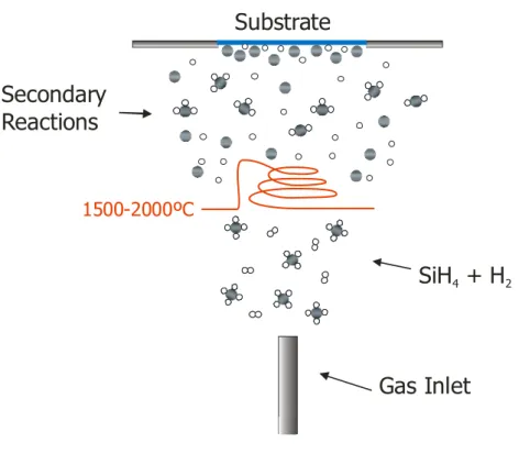
The deposition mechanism in Hot-Wire CVD can be schematically observed in Fig. 1.2, where the most remarkable features have been represented. Silane (SiH4), or a mixture of
silane and hydrogen (SiH4/H2), is introduced into the vacuum chamber, where a filament is
resistively heated up to temperatures between 1500-2000ºC. Those molecules impinging on the hot filament are dissociated by means of a catalytic process, after which mainly atomic hydrogen (H) and atomic silicon (Si) are released from the filament surface. The processes taking place at the filament surface have been analysed to identify the nature of the resulting species [Doyle et al. 1988]. On the other hand, and despite the fact that electron current is emitted by the hot filament, no ionisation has been observed. Thus, the energy of emitted electrons is not enough to cause ionisation and no ions are involved in this technique, therefore reducing those drawbacks (mainly damage of the growing material) arising from their presence. Some of the silicon and hydrogen atoms released from the filament can reach the substrate without suffering any collision, whereas some other undergo secondary reactions as they diffuse from the filament to the substrate. Those gas-phase secondary reactions may occur with other radicals generated at the filament or with SiH4/H2 molecules introduced into the reactor chamber. Products resulting from those
reactions and reaching the substrate affect the a-Si:H properties dramatically. In particular, high mobility radicals (SiH3, Si2H4) lead to better material properties than those observed
when dealing with species exhibiting high sticking coefficients (Si). Thus, whereas the former result in compact and dense structures, the latter lead to highly porous layers due to shadowing effects.
Substrate
SiH + H
4 2 1500-2000ºCGas Inlet
Secondary
Reactions
Figure 1.2. Schematic representation of the processes involved in the Hot-Wire CVD technique.
The quality of Hot-Wire CVD thin films depends critically on the deposition parameters, especially on the substrate temperature (Ts), which clearly determines the surface mobility
of radicals, and on those parameters influencing the nature of the radicals (pressure (P), filament temperature (Tf) and hydrogen-silane mixture (SiH4/H2)). Moreover, geometrical
issues such as filament-substrate distance (df-s) or filament features (area, shape) play also
a role on gas-phase and deposition chemistry. Details regarding the effect of the different parameters on the material properties will be presented in the following chapters. Special attention must be paid to Ts, as it limits the kind of substrate that can be used. Low cost
substrates, which can not stand high temperatures, are desirable to reduce fabrication costs. Regrettably, several results point to the lower mobility of major growth precursors in Hot-Wire CVD when compared with PECVD [Molenbroek et al. 1996, Schröder and
1. Introduction
Bauer 2000], so that high Ts values seem to be required. Nevertheless, some recent efforts
have been made to improve the performance of solar cells grown at moderate substrate temperatures by Hot-Wire CVD [Bauer et al. 1998, Van Veen and Schropp 2003], which have led to acceptable photovoltaic performances.
So far, only a few groups have reported results on completely Hot-Wire CVD deposited solar cells [Wang et al. 2000, Weber et al. 2000, Mahan et al. 2002, Kupich et al. 2003], as the deposition of doped layers has been typically carried out by means of alternative techniques (mainly PECVD) [Nelson et al. 1994, Conde et al. 2001, Van Veen and Schropp 2002, Ide et al. 2003]. Nevertheless, initial η above 8% have been reported for entirely Hot-Wire deposited devices [Wang et al. 2000, Weber et al. 2000] indicating the ability of this technique to produce solar cells with satisfactory performance. Additionally, some recent results have focused attention on the deposition of device-quality a-Si:H by Hot-Wire CVD at very high deposition rates (> 50 Å/s). The ability to produce solar cells with acceptable performance at much higher velocities than those commonly associated to PECVD has been demonstrated [Molenbroek et al. 1997, Mahan et al.2001, Mahan et al. 2001b]. Regrettably, relatively high Ts values have been commonly required for the
deposition of high-quality intrinsic a-Si:H by Hot-Wire CVD [Feenstra et al. 1999, Wang et al. 2000]. In that sense, low Ts (≤ 200ºC) was mainly employed throughout our work,
considering the future use of low-cost substrates.
1.4. Thin film silicon solar cells technology
The gradual reduction in production costs has driven photovoltaics research to the field of thin film deposition. As previously stated, silicon is the most studied material due to its suitable optoelectronic properties and its abundance in nature. In particular, a-Si:H has been widely used over the last decades in photovoltaic applications.
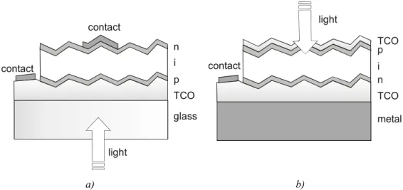
Two main structures are used in a-Si:H based solar cells: superstrate structure (Fig. 1.3(a)), where a p-i-n cell is deposited onto a transparent conductive oxide (TCO), and substrate structure (Fig. 1.3(b)), in which an n-i-p sequence is grown on a metallic substrate.
TCO n i p contact TCO metal light light TCO n i p contact contact glass a) b)
Figure 1.3. Schematic representation of the structure of p-i-n (a) and n-i-p (b) solar cells.
In order to enhance the collection of holes, which are collected at the p-layer, and whose mobility is smaller than that of electrons, illumination is commonly performed through the p-type layer in both cases. Some of the advantages associated to the superstrate geometry are the easy encapsulation process and the usually higher conversion efficiencies. In this case, enhanced η values are commonly a consequence of the relatively simple application of light confinement strategies [Rech and Wagner, 1999]. On the other hand, one of the main drawbacks related to this structure is the Ts limitation on the i-layer deposition, as
submission to high temperatures deteriorates the properties of the already deposited TCO and p-type layers. Regarding the substrate (or n-i-p) structure, a variety of substrates can be used as not such demanding requirements as in the superstrate geometry are needed. In particular, the substrate does not need to be transparent, so low-cost substrates such as stainless steel or plastic can be used. Moreover, this structure allows the use of high Ts for
the deposition of the i-layer, as the p-type one is deposited afterwards.
More complex structures, where semiconductor materials exhibiting different band gaps are combined (stacked cells), result in higher efficiencies, as this strategy allows a better coverage of the solar spectrum. In that sense, micromorph solar cells, which consist of multi-junction solar cells where both µc-Si:H and a-Si:H are used, showed its potential [Meier et al. 1997, Saito et al. 1998]. Hence, micromorph photovoltaic devices with conversion efficiencies around 14% have already been reported giving evidence of light absorption enhancement [Yamamoto 2002].
1. Introduction
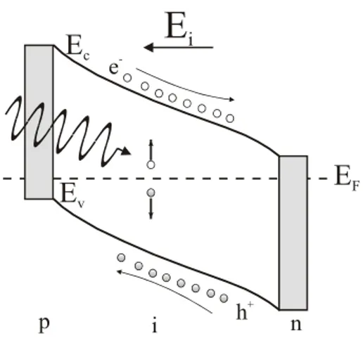
But, how do thin film solar cells work? The basic performance of thin film photovoltaic devices is based upon the properties of the different semiconducting materials. A schematic view of the band diagram describing the operation mode of a solar cell can be observed in Fig.1.4.
E
F p i nE
i h+ e-E
cE
vFigure 1.4. Schematic band diagram of a p-i-n junction solar cell. Ei is the internal electric field whereas Ec,
Ev and EF stand for conduction band, valence band and Fermi level respectively.
Carriers are mainly generated in the intrinsic layer, where the incoming light generates electron/hole pairs. Both electrons and holes are separated by the internal electric field (drift current), which is built by the doped layers (p- and n-type) at each side of the intrinsic material. Electrons are drifted to the n-type layer, whereas holes, which exhibit lower mobility, are driven towards the p-type one. The geometry presented favours an increased production of electron-hole pairs near the p-i interface, so that hole collection is facilitated by reducing their mean collection distance.
Some techniques have been developed to optimize the photovoltaic performance of solar cells. Thus, it is important to note that carriers generated in the doped layers do not contribute to the measured current, as the doped material density of defects is too large to allow carrier transport. As a consequence, light absorption in the p-type is to be minimized. In that sense, a clear improvement in solar cell performance can be observed after the use of an alloy of a-Si:H and carbon (a-SiC:H) [Fischer 1994, Merten 1996]. By the addition of carbon, the optical band gap is increased (up to 2 eV), so that low absorption in the p-type layer is obtained. The texturation of the surface is also known to play a key role in the optimization of solar cell performance. Regardless the structure (p-i-n, n-i-p, stacked cells),
texture favours the creation of electron-hole pairs by increasing the mean optical path of incoming photons, thus leading to increased absorption probability. Accordingly, the incorporation of a back reflector also results in larger optical paths, and consequently, in increased current generation.
1.5. a-Si:H at Universitat de Barcelona
Hydrogenated amorphous silicon has been studied for years at Universitat de Barcelona. Early studies were performed in the late 1980s, when the first device-quality layers were obtained by PECVD [Andújar 1990]. Moreover, encouraging results were also achieved for both thin film transistors (TFT) and solar cells. Different characterization systems were also developed to determine the optoelectronic properties of the material [Kasaneva 1990, Serra 1991]. a-Si:H solar cells were lately extensively produced and characterized by [Asensi 1994], whose efforts were centred in both the growth and numerical simulation of a-Si:H solar cells obtained by PECVD. Photovoltaic devices with initial efficiencies around 6% were obtained in those studies. a-Si:H photodiodes were also obtained and characterized [Puigdollers 1995], allowing a deep understanding on the doping of a-Si:H. On the other hand, the deposition of heterojunction solar cells with carbonized amorphous silicon p-layers was later introduced [Merten 1996]. This procedure allowed the initial conversion efficiency to reach values around 8.5%.
As far as Hot-Wire CVD is concerned, first studies at Universitat de Barcelona were carried out in 1994, when microcrystalline silicon layers were first deposited in Europe [Cifre et al. 1994]. A very elementary set-up was used, but satisfactory microstructural properties were achieved at high deposition rates (tens of Å/s). Besides, both p- and n-type doping of microcrystalline silicon layers after the addition of controlled amounts of doping gases (diborane for p-type and phosphine for n-type) to the SiH4/H2 mixture was later
developed [Puigdollers et al. 1995]. After those first and promising results, a new ultra-high vacuum Hot-Wire CVD reactor was built [Peiró 1999]. That reactor is currently operative and has been used throughout the present work. First studies performed in the new set-up were based on the deposition of µc-Si:H and nc-Si:H and the corresponding photovoltaic devices [Peiró 1999, Voz 2001]. Solar cells with initial conversion efficiencies around 3% were obtained with p-i-n structures entirely deposited by Hot-Wire
1. Introduction
CVD on ZnO:Al coated glass. Finally, recent results led to nc-Si:H solar cells exhibiting efficiencies around 5% after optimisation of the deposition parameters and technological modifications [Fonrodona 2003].
1.6. Aim of this work
The aim of the work presented in this thesis was twofold, as both material and device investigation was carried out.
Our first goal was to develop amorphous silicon (both intrinsic and doped) by Hot-Wire CVD with suitable properties for application in photovoltaic devices. Consequently, the role of the deposition parameters (filament temperature, pressure or hydrogen dilution), as well as that of geometrical considerations, had to be analysed. Furthermore, the use of low substrate temperatures (Ts ≤ 200ºC) was selected to allow the future employment of
low-cost substrates.
As far as the development of solar cells is concerned, our main objective was the growth of our first a-Si:H based devices totally deposited by Hot-Wire CVD. In particular, p-i-n structured solar cells grown on transparent substrates were investigated. Moreover, preliminary results concerning light trapping strategies, such as the use of textured substrates or the implementation of back reflectors, were also considered.
2. The Hot-Wire CVD reactor.
Characterization techniques
This chapter describes both the Hot-Wire CVD reactor at Universitat de Barcelona and the experimental techniques used to analyse structural, optical and electrical properties of the deposited layers. Additionally, techniques involved in the characterization of photovoltaic devices are also described.
2.1. The Hot-Wire CVD reactor
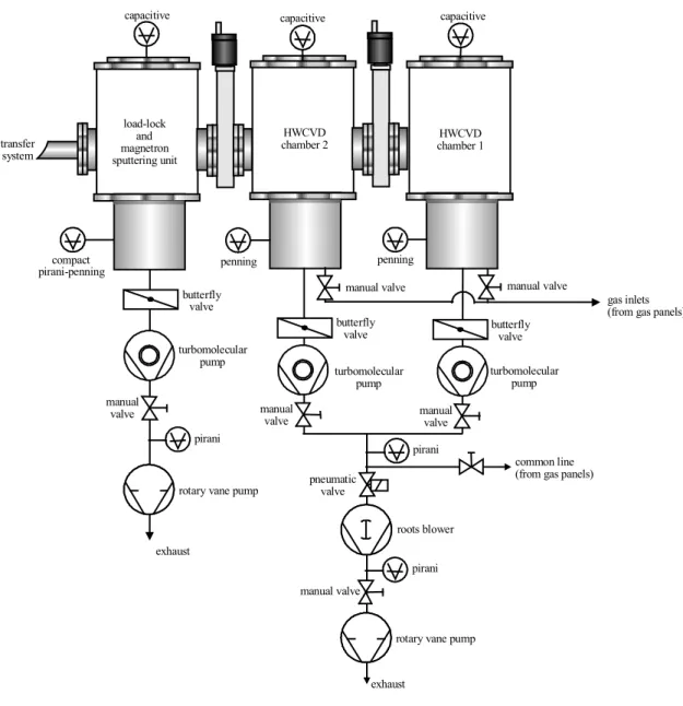
All samples presented in this work have been deposited in a Hot-Wire CVD set-up that was designed and built at Universitat de Barcelona in the frame of the CRYSTAL project within the JOULE programme of the European Commission. A detailed study regarding the design and the implementation of the system can be found in [Peiró 1999], so only the general architecture and the most significant features will be remarked here.
The Hot-Wire CVD system employed in this work consists of three isolated ultra-high vacuum chambers. Hydrogen (H2) and silane (SiH4) are used as precursor gases to grow
silicon thin films, whereas the addition of either diborane (B2H6) or phosphine (PH3)
allows the deposition of p- and n-type doped material respectively. An overview of our Hot-Wire CVD set-up is presented in Figure 2.1. A load-lock chamber is used to prevent the deposition chambers from being exposed to air, which could accentuate contamination due to oxygen and water vapour. In that same direction, a feedgas purifier is used in the silane and hydrogen lines to prevent contamination due to impurities (mainly oxygen and carbon) coming from the gas lines [Torres et al. 1996]. On the other hand, two isolated chambers are used to deposit thin films by Hot-Wire CVD. Both chambers exhibit mainly the same equipment, though one of them is used for intrinsic material whereas the other one is exclusively devoted to the growth of doped layers. The use of two different reactors prevents cross-contamination problems linked to memory effects in the chamber, which result in worse active layer properties. This issue has been shown to be especially dramatic when dealing with nc-Si:H technology [Voz et al. 2000], as even low impurity concentrations can make the intrinsic material unsuitable for its use in solar cells.
2. The Hot-Wire CVD reactor. Characterization techniques
Furthermore, a radio frequency (RF) magnetron sputtering system was also installed in the load-lock chamber. This system allows the growth of both aluminium-doped zinc oxide (ZnO:Al) and indium tin oxide (ITO). Both materials are well-known transparent conductive oxides (TCO) and have been extensively incorporated as contacts in photovoltaic devices.
The inline configuration of our system allows the growth of either TCO/p-i-n/metal or metal/n-i-p/TCO structures with no air-breaks between the deposition of the different semiconducting layers (p-type, intrinsic and n-type), thus minimizing oxidation and contamination coming from the atmosphere.
pneumatic valve manual valve manual valve manual valve manual valve manual valve pirani pirani pirani penning compact pirani-penning capacitive capacitive gas inlets (from gas panels)
common line (from gas panels) butterfly
valve turbomolecular
pump
rotary vane pump roots blower rotary vane pump
exhaust exhaust turbomolecular pump butterfly valve manual valve penning capacitive butterfly valve turbomolecular pump HWCVD chamber 2 load-lock and magnetron sputtering unit HWCVD chamber 1 transfer system
Regarding the pumping system, both a turbomolecular and a rotary vane pump are incorporated in the load-lock chamber, whereas an additional roots blower is used in the Hot-Wire CVD reactors. The addition of a roots blower between the turbomolecular pumps and the rotary vane pump permits the introduction of higher gas flows into the Hot-Wire CVD chambers. Base pressures around 10-7 mbar are achieved in the load-lock chamber, whereas values in the order of 10-9 mbar can be reached in the Hot-Wire CVD reactors.
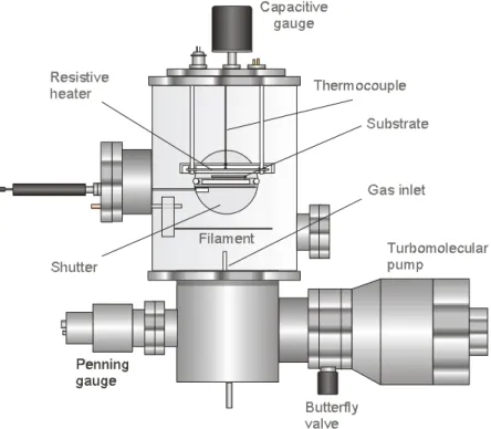
The internal arrangement of the Hot-Wire CVD chambers is seen in Figure 2.2. Both reactors (intrinsic and doped) exhibit a similar distribution, so only one scheme is presented. A single tungsten (W) or tantalum (Ta) filament is used as the catalytic element with temperatures ranging from 1500ºC to 1900ºC. Ta results especially suitable at low filament temperatures (Tf), as the formation of silicides on its surface is lower than that
observed in tungsten filaments [Van Veenendaal et al. 2001]. The formation of silicides lowers the lifetime of the wires, as their presence increases the wire brittleness. Accordingly, breakage typically occurs at the cold ends of the filament, where silicides are mainly formed [Ishibashi 2001, Mahan 2003]. On the other hand, W seems to be preferable when working at high temperatures due to its higher endurance to deformation.
2. The Hot-Wire CVD reactor. Characterization techniques
An internal heater (as seen in Fig. 2.2) is used to increase the substrate temperature (Ts) in
the doped material chamber, whereas an external one is arranged in the intrinsic material reactor [Fonrodona 2003]. An external heater is intended to minimize contamination effects, which might clearly degrade the properties of the active layer and, eventually, limit the solar cell performance [Stöger et al. 1999, Schlosser et al. 2000, Voz et al. 2000b]. Besides, a proportional-integral-derivative (PID) control is used to determine the power supplied to the corresponding heaters. It is important to remark that the actual substrate temperature (Ts) can not be straightforwardly determined, as it can be dramatically affected
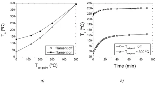
by radiation from the filament. In order to estimate its value, a calibration procedure taking into account the filament influence was performed. Thus, a thermocouple was attached to a glass substrate, whereas similar pressure (P = 1×10⁻² mbar) and filament temperature
(Tf = 1640ºC) to those employed in our experiments were selected. Moreover, a linear Ta
wire was used. The resulting calibration curves can be observed in Fig. 2.3.
0 20 40 60 80 100 25 50 75 100 125 150 175 200 225 250 275 0 100 200 300 400 500 0 50 100 150 200 250 300 350 400 T s (º C ) filament off filament on T s (ºC)
Tset-point (ºC) Time (min)
Tset-point off
Tset-point = 300 ºC
a) b)
Figure 2.3. Calibration of Ts as a function of the set-point temperature (a). Time evolution of Ts for two
different temperatures evidencing the dramatic influence of the filament, especially at low temperatures (b). P = 1×10⁻² mbar, T
f = 1640ºC and φH2 = 20 sccm were used for all measurements.
Data presented in Fig. 2.3 evidenced a remarkable influence of the filament radiation on Ts
when low temperatures were considered. Hence, Ts reached a value around 125ºC when
the heater was off. Conversely, lower Ts values than those expected were achieved at the
highest temperatures considered (Ts ~ 400ºC for Tset-point = 500ºC or Ts ~ 250ºC at Tset-point
(especially at low temperatures), the term Ts will refer to the set-point values from now on.
In fact, most of the samples presented in this work were grown at substrate temperatures between 125 and 200ºC, for which the Ts values were fairly close to Tset-point.
2.2. Characterization techniques
Different characterizations techniques were employed throughout this work to determine the properties of a-Si:H layers. Thus, structural, electrical and optical properties were analysed as they all bring some additional insight into the material features.
2.2.1. Structural characterization
The thickness of the deposited samples was measured by means of a Dektak 3030 stylus profilometer, from which the growth rate (rd) was evaluated after taking into account the
deposition time.
- Fourier Transform Infrared (FTIR) Spectroscopy
Fourier Transform Infra-Red Transmittance of silicon thin layers was measured by means of a Nicolet 5ZDX FTIR spectrometer. Incorporation of oxygen into the samples after exposure to air, concentration of bonded hydrogen, and hydrogen bonding configuration could be determined from the obtained spectra.
Device-quality material exhibits a compact structure, so oxygen is not expected to diffuse into the material, even after prolonged exposure to atmosphere. The incorporation of oxygen in silicon thin films can be detected by the presence of an absorption band around 1100 cm-1 associated to Si-O bonds [Curtins and Veprek 1986]. Moreover, enhanced oxidation experiments after light exposure (photoxidation), which is known to accelerate the process, were also performed.
Additional insight into the microstructure of the material can be gained by considering the hydrogen-bonding configuration. An important absorption band centred at 2000 cm-1 corresponding to hydrogen in monohydride bonds (Si-H) can be typically observed in
2. The Hot-Wire CVD reactor. Characterization techniques
device-quality a-Si:H, whereas hydrogen bonded in either multihydrides (SiH2 or SiH3) or
internal voids gives rise to a contribution around 2100 cm-1 [Lukovsky et al. 1979]. Therefore, low signals around 2100 cm-1 are required to ensure compactness of the growing material. A quantitative approach is then given by the microstructure factor (R*)
(2.1) R I I I * = + 2100 2000 2100
where Ik represents the integrated absorption of the corresponding bands
∫
= Band i i d I ω ω ω α ( ) (2.2)As previously stated, a dominant absorption band around 2000 cm-1 is desirable and, consequently, low R* values (R* < 0.1) are required.
Finally, hydrogen density (NH) can be evaluated from the absorption band at 630 cm-1
NH = A·I630 (2.3)
where A = 2.1×1019 cm-3 [Langford et al. 1992] and I
630 is the integrated absorption of the
corresponding band. The peak around 630 cm-1 includes the rocking modes of bonded hydrogen in every possible configuration, so the totality of bonded hydrogen atoms is taken into account. In order to obtain the hydrogen content (CH), a value of 5×1022 cm-3 for
the silicon density (NSi) has been commonly accepted, so CH results
100 × + = H Si H H N N N C at % (2.4) - Raman spectroscopy
Raman spectroscopy experiments were performed to determine the crystalline fraction (Xc’) of the samples. Although our work was mainly focused on a-Si:H, those deposition
material exhibiting very promising properties [Guha et al.1999]. Moreover, different research groups have shown the potential of p-type nanocrystalline layers when incorporated into solar cells [Guha et al. 1986, Rath and Schropp 1998], so their properties were also evaluated in the present work.
A Jobin-Yvon T64000 Spectrometer with a laser beam at a wavelength of 514 nm was employed. The characteristic peak corresponding to the transverse optical (TO) mode of crystalline silicon can be found at 520 cm-1, whereas the amorphous band appears around 480 cm-1. Deconvolution of the observed bands allows the calculation of X
c’ by applying a c c c I I I X σ + = ' (2.5)
where Ic and Ia are the integrated intensities of the amorphous and crystalline contributions,
and σ is the cross section for the Raman effect in a-Si:H and nc-Si:H, which takes into account the crystallite size [Bustarret et al. 1988]. Additional peaks centred between 500 and 510 cm-1, which are mainly attributed to grain boundaries effects, are also considered by different groups [Han et al. 2003, Van Veen 2003]. In our case, the crystalline ratio (Xc), instead of the crystalline fraction, was defined and will be used throughout this text as
an objective indicator of the crystallinity of the samples. It was defined as
480 520 520 I I I Xc + = (2.6)
where Ik refers simply to the integrated contribution at either 480 or 520 cm-1. From now
on, to facilitate intuitive comprehension, the denomination crystalline fraction will, in fact, refer to Xc instead of Xc’.
2.2.2. Electrical characterization
A detailed study regarding electrical characterization techniques can be found in [Voz 2001]. In this section, only a few words will be given concerning those techniques involved in our research. Both dark conductivity (σ) vs. temperature and steady state
2. The Hot-Wire CVD reactor. Characterization techniques
photoconductivity (SSPC) were measured after deposition of the corresponding coplanar electrodes. These electrodes were obtained by thermal evaporation of aluminium (Al), their length was 10 mm and the distance between them 1 mm. On the other hand, electrical properties in the direction perpendicular to the substrate were measured for doped samples deposited on both stainless steel and TCO (ZnO:Al in our case) coated glass.
- Dark conductivity
Dark conductivity as a function of temperature was measured for all samples under study. Experiments were carried out under vacuum to eliminate moisture, which might lead to superficial conduction. The measured trend was fitted according to the well-known conductivity (σ) dependence on temperature (T)
− = T k E B A exp 0 σ σ (2.7)
where kB is the Boltzmann constant and EA, the activation energy, which is used as an
indication of the Fermi level position. Dark conductivity at room temperature (σd) and EA
were taken as significant parameters. Low σd and EA around midgap are expected for
device-quality intrinsic a-Si:H, whereas high σd and low EA are required for doped layers.
- Steady State Photoconductivity (SSPC)
Steady State Photoconductivity (SSPC) experiments were carried out by using the same electrode geometry as that employed for dark conductivity measurements. The photoconductivity of a sample corresponds to the relative change in its electrical conductivity when it is illuminated. In particular, σph corresponds to the measured
conductivity at standard illumination conditions (100 mW/cm2). SSPC experiments allowed the evaluation of the mobility-lifetime product (µτ), which deals mainly with the transport properties of majority carriers [Voz 2001]. High mobility and lifetime are expected, so that elevated µτ values are desirable. Nevertheless, σph and µτ are
when a Fermi level shift occurs as a consequence of the incorporation of contaminants (which are also known to increase σd). Thus, σph and µτ values must be considered jointly
with σd, so that only samples exhibiting high σph (and µτ) values and low σd (indicating
they are highly intrinsic) are suitable for its use in solar devices.
Regarding the above-mentioned relation between σph (µτ) and σd, the suitability of the
material can be quantified by means of the Photoresponse (S), which considers the electrical properties under illumination and dark conditions. S is then simply defined as
Photoresponse = S = σph / σd (2.8)
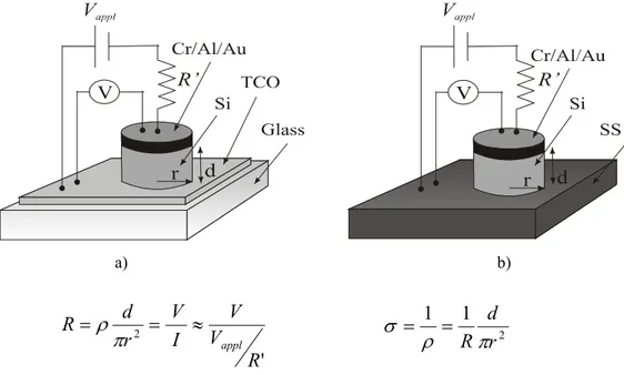
- Electrical measurements in the direction perpendicular to the substrate
Electrical behaviour in the direction perpendicular to the substrate was evaluated for doped samples grown on conductive substrates, namely, ZnO:Al coated glass and stainless steel. Electrical conduction in solar cells takes place in this direction, so such electrical properties, which quite often are forgotten, must be analysed. The geometry and the experimental set-up for these measurements can be seen in Fig. 2.4.
a) b) ' 2 R V V I V r d R appl ≈ = = π ρ 2 1 1 r d Rπ ρ σ = =
Figure 2.4. Electrical measurements in the direction perpendicular to the substrate for doped layers
2. The Hot-Wire CVD reactor. Characterization techniques
The conductivity perpendicular to the substrate (σ⊥) was evaluated by taking into account
the measured resistance and the geometry used. Cr/Al/Au circular electrodes were evaporated on both p- and n-type doped layers. Small area electrodes were used and dry etching was performed by means of a CF4 plasma to avoid current losses. Moreover, four
probes were used to minimize effects arising from the electrode-probe contact. A voltmeter was used to determine the voltage drop (V), whereas current (I) was determined from the applied voltage (Vappl) and R’ (1MΩ) after considering much less resistive losses in the
silicon film. It is important to remark that electrical properties perpendicular to the substrate might be clearly influenced by both the junction characteristics and the structural features of the sample at its initial stages of growth. Thus, σ⊥ cannot be compared with σd,
as the latter can be considered as a property of the material, whereas the former might be clearly affected by the junction properties.
2.2.3. Optical characterization
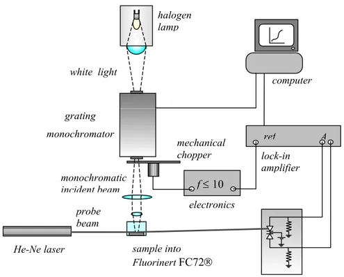
Optical properties were analysed by means of Photothermal Deflection spectroscopy (PDS), which allowed the evaluation of the optical behaviour even for very low absorptions (αd < 10-5). A diagram of the PDS set-up is presented in Fig. 2.5, where the
arrangement of the different elements is observed. An overview of the physical basis will be shown below, whereas deeper understanding on the experimental issues and the calculation of the optical absorption coefficient (α) can be obtained from [Voz 2001].
In PDS, the layer under study is submerged into a liquid (Fluorinert FC72TM by 3M in our set-up), whose refractive index exhibits a clear thermal dependence. A monochromator is used to select the wavelength of the radiation reaching the sample, which absorbs a fraction of the incident light. The absorbed light induces a heating of the sample by non-radiative recombination. The increasing temperature of the layer causes a temperature gradient in the liquid, so the refractive index also experiences a variation. This gradient leads to the deflection of the laser beam as seen in Figure 2.5, which can be quantified by means of the corresponding detector. Moreover, the monochromatic light is chopped, so very low signals can be detected with the help of a lock-in amplifier. In summary, the more incoming light is absorbed, the more deflected the laser beam is, and, consequently, the higher the measured signal results.
halogen lamp He-Ne laser mechanical chopper electronics probe lock-in amplifier f ≤ 10 deflection detector A ref beam monochromatic incident beam sample into Fluorinert FC72 white light grating monochromator computer
Figure 2.5. Overview of the PDS set-up in our laboratory.
The accuracy of PDS is lowered at high optical absorptions, so that PDS measurements have to be complemented with standard transmission measurements. These measures allow determining the absorption spectrum in the whole visible range, so all optical information becomes available. A typical spectrum for an a-Si:H sample is presented in Fig. 2.6.
1.0 1.2 1.4 1.6 1.8 2 .0 2.2 100 101 102 103 104 105 defects absorption Urbach Front hν (eV) α (c m -1 )
2. The Hot-Wire CVD reactor. Characterization techniques
The optical gap (Eg) can be evaluated from the high-energy range by fitting the curve to the
well-known Tauc’s law [Tauc 1974]
(2.9) (α ν)12 =c( ν −E )
g
h h
where c is a constant. On the other hand, optical transitions caused by localized states in the band tails give rise to the Urbach front in the region before the optical gap [Bustarret et al. 1988b]. This region can be fitted by using the following relation
= v BT k hν α α 0exp k TB v ≡Eu (2.10)
The determination of the characteristic Urbach energy (Eu) gives some insight into the
structural disorder of the sample, as localized states are correlated to the dispersion in both bond angle and bond distance.
Finally, absorption in the low-energy range permits the determination of the defect density in the mid-gap region, which are mainly provoked by dangling bonds
[
]
∫
〈 − = g E E u d C E E dE N α( ) α ( ) (2.11)where αu (E) represents the extrapolation of the Urbach edge for lower energies and C is a
proportionality constant with a value of 7.9×1015 cm-2eV-1 [Jackson and Amer 1982].
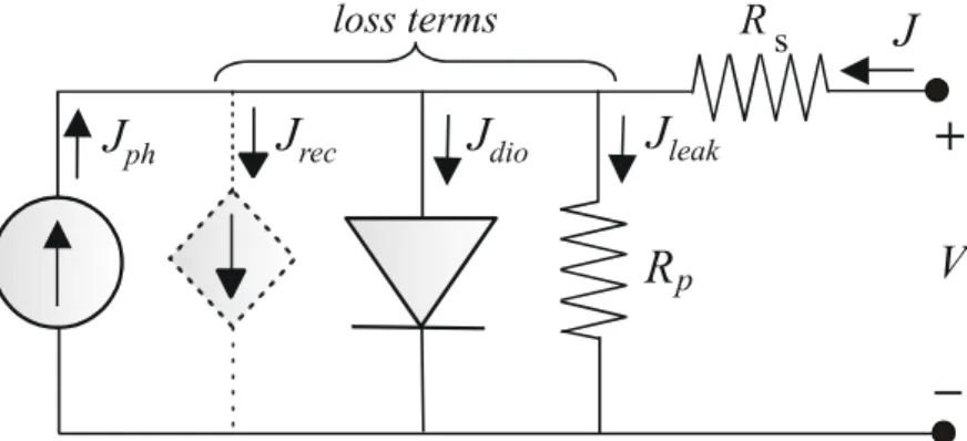
2.3. Device characterization
The use of equivalent circuits is an enlightening approach to describe the performance of electronic devices. The photovoltaic performance of a solar cell can be simply modelled by the electric equivalent circuit shown in Fig. 2.7, where both the diode term and the photocurrent source correspond to the behaviour of an ideal solar cell. Leakage currents are represented by the parallel resistance (Rp, which should be infinite in the ideal case),
whereas the series resistance (Rs) corresponds to resistive losses in both external contacts
by recombination in the intrinsic layer due to the presence of defects. Thus, Jrec is expected
to depend clearly on the illumination intensity, as more recombination is observed when higher concentration of photogenerated carriers is considered.
Figure 2.7. Electric equivalent circuit of a solar cell consisting of a current source (Jph), a diode (Jdio),
series (Rs) and parallel (Rp) resistances and the recombination current term (Jrec).
The typical current density (J) vs. voltage (V) characteristic can be analytically obtained from the previous model, leading to the following expression
(
)
p s e nkT JR V o bi s bi c ph ph leak dio rec ph R JR V e J V JR V V V J J J J J J V J s − + − + − − ⋅ ⋅ + − = = + + + − = − 1 1 1 ) ( ) / /( ) ( (2.12)where di is the thickness of the intrinsic layer, Vbi the built-in voltage, Jph the generated
photocurrent density and, Jo and n the inverse saturation current density and the ideality
factor of the diode respectively. Besides, Vc is the collection voltage, which is linked to the
intrinsic layer conduction properties.
The first term on the right in equation 2.12 corresponds to the photogenerated current density. The other three terms deal with recombination (Jrec), diode (Jdio) and leakage (Jleak)
current densities respectively. It is worth mentioning that “Jk” is employed for current
densities, whereas Ik is typically employed when referring to total current values. Results
presented in this work are always referred to current density measurements, so “J” will be used throughout this text instead of “I”.
2. The Hot-Wire CVD reactor. Characterization techniques
- Current density versus voltage measurements
The fundamental measurement to analyse the performance of a solar cell is the J(V) curve, that is, the current density dependence on the voltage applied, from which the parameters that determine the solar cell performance are derived: open circuit voltage (Voc), short
circuit current density (Jsc), fill factor (FF) and conversion efficiency (η). In particular,
measurements are commonly performed at standard illumination conditions, for which an intensity of 100 mW/cm2 is considered. FF is defined as the ratio of P
max (maximum power
density) to the product Voc·Jsc, whereas the conversion efficiency corresponds to the ratio
of Pmax to the incident power density
light oc sc light oc sc P V J FF P P V J P FF · · · max max = = = η (2.13)
Additionally, both the short-circuit (Rsc) and the open-circuit (Roc) resistances are
evaluated oc oc sc sc dI dV R dI dV R = = (2.14)
The experimental set-up and an example of a J(V) curve, where the above-mentioned parameters are illustrated, can be observed in Fig 2.8.
- Variable Illumination Measurements (VIM)
Useful information can be extracted from J(V) curves measured under a wide range of illumination levels, the so-called VIM method, by taking into account the equivalent circuit shown in Fig. 2.7. The same experimental set-up as when dealing with J(V) curves under standard illumination is employed, and light intensity is simply varied by means of grey filters (Fig. 2.8). A detailed study on the VIM method and the interpretation of the corresponding results can be found in [Merten et al. 1998], so only a brief explanation will be given in this chapter.
voltmeter device halogen lamp computer −
R
four quadrant voltage source J-V converter ideal amperimeter grey filters (VIM measurements)J
dR
V
a) 1/Roc 1/Rsc 0 0 Vmax Jmax Pmax Voc Jsc V J sc ocJ V P FF= max inc sc oc P FF J V = η b)Figure 2.8. Experimental set-up for the acquisition of J(V) curves (a) and example of a J(V) curve and the
characteristic parameters calculated from it: Voc, Jsc, FF,Rsc,Roc and η (b).
Different regimes can be observed as the illumination level is varied (Fig. 2.9). In order to analyse the obtained results, Voc, FF, Rsc and Roc are evaluated for all the illumination
2. The Hot-Wire CVD reactor. Characterization techniques
the study of different technological and material effects that determine the solar cell performance. C u rr ent Voltage Illumination Intensity C u rr ent Voltage Illumination Intensity
Figure 2.9. Different regimes can be observed in the J(V) curve as a function of the illumination level.
The low illumination regime is mainly determined by Rp, whereas Rs becomes dominant at
very high illumination levels. At standard illumination levels, parasitic resistances are expected to be negligible, so the solar cell performance is controlled by the p-i-n junction physics and the properties of the different semiconducting layers. Measurements performed in this range allow the study of both the diode (Io, n) and the recombination
current term (Vc) in equation 2.12, which clearly determine the solar cell response. In
summary, VIM accounts for both physical (diode behaviour, recombination in the intrinsic layer) and technological issues (Rp, Rs), thus giving quite a complete insight into the device
performance.
- Spectral Response
Spectral response measurements are performed to get more detailed information on the current generation process. In spectral response experiments, the photovoltaic response as a function of the incoming light wavelength is measured, so that the generated photocurrent (Jph) is evaluated as a function of the wavelength of the incoming
monochromatic beam. The external quantum efficiency is then evaluated according to the following formula det det EQ J J EQ= ph (2.15)
where Jph and Jdet are the measured photocurrents for the solar cell under study and the
calibration detector respectively, and EQdet is the external quantum efficiency of the
calibrated detector. EQ correlates the electron/hole pair collected per incoming photon. A clear reduction in EQ is observed at both extremes of the working range. Low energy photons (energy lower than the band gap of the active material) cannot create electron/hole pairs and EQ tends to zero. On the other side of the spectrum, high-energy photons create a large number of electron/hole pairs in the p-type zone. These carriers cannot be efficiently collected due to the poor transport properties of the p-type layer so EQ tends to zero as well. In summary, spectral response measurements allow the identification of critical points (or bottlenecks) that limit the performance of the solar cells under study. Abnormally low EQ values in the low energy range point to collection difficulties in the bulk, which are indicative of problems in the intrinsic material and/or in the internal electric field. On the other hand, too low responses in the high energy range account for collection problems at the p-type layer or at the p/i interface.