Alternative Substrates for Sustainable
and Earth-abundant Thin Film Photovoltaics
Ignacio Becerril Romero
Aquesta tesi doctoral està subjecta a la llicència Reconeixement 4.0. Espanya de Creative
Commons.
Esta tesis doctoral está sujeta a la licencia Reconocimiento 4.0. España de Creative
Commons.
Autor: Ignacio Becerril Romero
Directors: Dr. Edgardo Saucedo Silva i Dr. Paul Pistor
Tutor: Prof. Dr. Alejandro Pérez-Rodríguez
Alternative Substrates for
Sustainable and Earth-abundant
Thin Film Photovoltaics
Memòria presentada per optar al grau de doctor per la
Universitat de Barcelona
Programa de doctorat en
Enginyeria i Ciències Aplicades
Every human civilization has inevitably collapsed. Ours is not going to be different. However, this time we have the knowledge and capacity to decide how we want it to happen. Let’s make it softly, peacefully and living long and happy lives in harmony with nature.
Acknowledgments
I could not have done this thesis without the help, support, guidance and wisdom of many, many people. I will try to show my gratitude to all of them but, if I forget anybody, do not take it personally. My brain is really exhausted after the hard work of the last months.
I would like to start by thanking Edgardo for giving me the opportunity of doing my PhD studies in IREC under his supervision. Likewise, I would like to thank Paul, my second supervisor, for his knowledge and valuable inputs. I have learned a lot from you both and I hope I can keep learning from you in the future. Of course, I would also like to thank Alejandro, my thesis tutor, for his guidance and for always finding some time to help everybody despite the stress and the huge amount of work to which he is usually exposed.
Now, I will try to thank all the people with whom I have worked and/or that have contributed to this thesis either professionally, personally or both. For the sake of equality, I will stick to the following order:
1. IREC workers
a. Time-based: the different stage of the thesis in which I met you or work with you.
b. Alphabetically 2. Other places
3. Family and friends
IREC workers
Old times
Alex → Thank you for your unconditional friendship and support that, I am sure, will last for very long after you leave IREC and find your own way.
Diouldé → I could write at least 30 pages to express my sincere gratitude for everything you have done for me in the last years. Unfortunately, this thesis is already too long. You are an extraordinary person. Thank you for EVERYTHING.
Florian → Thank you for sharing with me so many nice moments inside and outside IREC and for being my sparring in the Kung Fu classes.
Haibing → You are an extremely gifted researcher and a super nice person. In addition, you are my ping pong and Kung Fu master. I appreciate all the time we have spent together. Thank you very much.
Laura → Thank you for being by my side (literally), for giving me so much support in my first two years in IREC and for not forgetting about me when you left.
Marcel → I have learned so much from you…: sputtering, guarradas, coffee, bikes… Thank you for that, for being such a nice and wise guy and for your invaluable support.
Markus → Thank you for teaching me so much, for your wisdom and for always being in a positive mood.
Max → Thank you for you calmed friendship, your nice company and your professionality. Moisés → I am very thankful for letting me continue your research on transparent substrates and use it for this thesis. Thank you also for everything else.
Mónica → Thank you for your friendship and for all the support you gave me at the first stages of my thesis.
Rokas → Thank you for eating pizza with me on Fridays in the old times, for your support (especially with the 5th chapter of this thesis) and for your friendship.
Sergio → Thank you for all these years working together, for all the times you have helped me and for all the nice moments we have shared.
Simón → I am very thankful to you. You were the person taking care of me in my first days in IREC with your special style (I still remember my first day when you bombarded me with all your research mixed with “mona” and “clin clin”) but with great research abilities. I owe you a lot about my research and way I do it which is clearly inspired in yours. In addition, you supported me from day one. Thank you very much.
Víctor → Thank you for your wisdom, your enthusiasm, your support, the Monday beers and for caring about me.
Yudania → Thank you for being always on my side supporting me, for teaching me all I know about chemical processing and for being the good person you are.
I would also like to thank other people from the old times in IREC with whom I shared part of my thesis: Cristina, Doris, Matías, Mirjana and Xavi.
More recent times
Jacob → Thank you for being my friend, for your scientific discussions, your company until 10 pm in the lab, for your support, for sharing so many things with me both inside and outside IREC, for always supporting me and for making me a part of your life.
Mohamed → Thank you for being always in a pleasant mood and for always thinking good of me.
Pedro → Thank you for your nice and relaxed character, for your support and for inviting me to join you so many times to smoke (even though I am not a smoker) and to other healthier activities.
Very recent times
Alex gallego → Thank you for your support and for being such a nice guy and a good colleague in the short time you have been in IREC.
Zak → Thank you for being there every single time I have asked you for help and for your knowledge and support.
I would also like to thank the newest guys, Kunal and Oriol, for being so nice to me during the little time they have been in IREC.
LATAM
Thanks to all the LATAM people in IREC for sharing with me their culture and friendliness. Esteban → Thank you for your friendship and for being always so kind and positive.
Jacob → See previous section. But also thank you for making me part of the LATAM community.
Parce → Thank you for being such a good friend and for sharing so much with me during the time you were here.
Roberto → Thank you for all the help you gave us, your professionality and for being such a nice person.
Thanks also to César and el Perú for the moments we have shared.
MASCIR
I would like to thank all the people in MAScIR for becoming my family during my secondment there: Prof Sekkat, Safae, Siham, Sara, Sanaa, Nadjet, Nada, Yahya, Tarik, Hatim and Abderrahim and, of course, to Zakaria.
A very special thanks goes to my dear Imad. Thank you for being such a good friend and colleague and for taking care of me in Morocco.
Others
Thanks to Diego and Iván, from UJI, for the ceramic substrates as well as for their help and friendliness during the ECOART project.
In addition, I would like to thank Alfonso for making me pass from looking comfortably into the abyss of growth, energy and sustainability to making me fall into it.
Finally, there is a person that should also be thanked because, without her, this and many scientific works would not be possible: Alexandra Elbakyan. Thanks for making science freely available for everybody, as it should be.
Family and friends
This work would have not been possible at all without the support given to me by my family and friends.
Thanks to my friends from Zaragoza: Alb, Basti, Blesa, Eric, Nacho y Quílez; for always being there when I needed them regardless our ups and downs.
I would of course like to thank my parents: my father José Luis and my mother Elda. All that I am and all that I have achieved is thanks to you. I will always be grateful to you. Likewise, I would also like to thank my sister Sofía, my grandmothers, Aurora y Ángeles, my grandfathers (wherever they are), Pepe y Pascual, and the rest of my family for everything they have done for me and given to me.
And, last but not least, thanks to my beloved wife Anita. Thank you for being always by my side, for suffering my grumpy mood all the times that I have been stressed (i.e. 90% of the days), for dealing with my frequent migraines, for helping me in every way you can, for caring so much about me and for your unconditional and true love.
Table of contents
Preface and publications _________________________________________________ i
Prefacio y publicaciones ________________________________________________ iii
List of acronyms and abbreviations _______________________________________ vii
Table of figures ________________________________________________________ x
List of tables _________________________________________________________ xvi
1.
Introduction ______________________________________________________ 1
1.1 Energy supply in a growth-addicted financial system: what is the role of
photovoltaics in all this? _____________________________________________________ 1 1.1.1 The threat of fossil-fuel dependence: the hidden link between economy, growth,
complexity and energy _____________________________________________________________ 1 1.1.2 Lights and shadows of photovoltaics: potential, EROI and limitations _________________ 4 1.1.3 Focus and motivation of this work _____________________________________________ 8 1.2 Fundamentals of solar cells _____________________________________________ 8
1.2.1 What is a solar cell and how does it work? ______________________________________ 8 1.2.2 Main parameters of solar cells _______________________________________________ 13 1.3 Photovoltaics: current commercial technologies and EROI ___________________ 15
1.3.1 1st generation PV: crystalline Si solar cells ______________________________________ 15 1.3.2 2nd generation PV: thin film solar cells _________________________________________ 17 1.4 Earth-abundant thin films: kesterite solar cells ____________________________ 22
1.4.1 Fundamental properties ____________________________________________________ 22 1.4.2 Evolution and state-of-the-art _______________________________________________ 23 1.4.3 Voc deficit: the main limitation of kesterites_____________________________________ 25
1.4.4 Alkali doping _____________________________________________________________ 28 1.4.5 Summary and final remarks _________________________________________________ 31 1.5 Context and objectives of the thesis _____________________________________ 31
1.5.1 The limitations of soda-lime glass and Mo ______________________________________ 31 1.5.2 Objectives of the thesis _____________________________________________________ 32
2.
Methodology ____________________________________________________ 34
2.1 Overview __________________________________________________________ 34 2.2 Techniques and pieces of equipment ____________________________________ 34 2.2.1 Structural, compositional and morphological characterisation______________________ 34 2.2.2 Optical and electrical characterisation _________________________________________ 41 2.2.3 Solar cell fabrication _______________________________________________________ 45 2.3 Solar cell fabrication procedure ________________________________________ 49
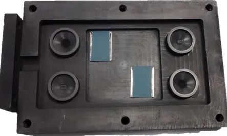
2.3.1 Substrate cleaning _________________________________________________________ 49 2.3.2 Back contact deposition ____________________________________________________ 50 2.3.3 Precursor deposition _______________________________________________________ 51 2.3.4 Absorber synthesis ________________________________________________________ 51
2.3.5 Chemical etchings for secondary phase removal _________________________________ 52 2.3.6 CdS buffer layer deposition __________________________________________________ 52 2.3.7 Window layer/front contact deposition ________________________________________ 53 2.3.8 Solar cell scribing and contact ________________________________________________ 53 2.3.9 Low temperature post-annealing treatment ____________________________________ 54
3.
CZTSe solar cells developed on polymer substrates: Effects of low-temperature
processing ___________________________________________________________ 55
3.1 Introduction ________________________________________________________ 55 3.1.1 Light-weight and flexible substrates for kesterite solar cells ________________________ 55 3.1.2 Polyimide: a promising and unexplored substrate ________________________________ 56 3.1.3 Limitations of polyimide and objectives of this work _____________________________ 57 3.2 Experimental _______________________________________________________ 58
3.2.1 Sample preparation ________________________________________________________ 58 3.2.2 Characterization __________________________________________________________ 62 3.3 Results ____________________________________________________________ 63
3.3.1 CZTSe on polyimide: alkali doping strategies ____________________________________ 63 3.3.2 Low temperature CZTSe on SLG: effect of processing temperature __________________ 68 3.3.3 Further strategies to increase conversion efficiency: higher temperatures and Na+Ge doping_________________________________________________________________________71 3.4 Discussion _________________________________________________________ 76
3.4.1 Alkali doping _____________________________________________________________ 76 3.4.2 Differences in the temperature-dependence of secondary phase-formation in soda-lime glass and polyimide substrates ______________________________________________________ 78 3.4.3 Origin and effects of SnSe2 __________________________________________________ 80
3.5 Conclusions ________________________________________________________ 83
4.
Vitreous enamel as sodium source for efficient kesterite solar cells on
commercial ceramic tiles _______________________________________________ 85
4.1 Introduction ________________________________________________________ 85 4.1.1 Building integrated photovoltaics _____________________________________________ 85 4.1.2 Solar tiles and thin film photovoltaics: a combination with great potential ____________ 88 4.1.3 Limitations of ceramic substrates for thin film deposition and objectives of this work ___ 88 4.2 Experimental _______________________________________________________ 89
4.2.1 Substrate description and sample preparation __________________________________ 89 4.2.2 Characterisation __________________________________________________________ 90 4.3 Results ____________________________________________________________ 90
4.3.1 Substrate and back contact analysis ___________________________________________ 90 4.3.2 Device analysis ____________________________________________________________ 95 4.3.3 Discussion _______________________________________________________________ 99 4.3.4 New batch of substrates and modified annealing _______________________________ 100 4.4 Conclusions _______________________________________________________ 105
5.
Transition metal oxides for kesterite solar cells developed on transparent
5.1 Introduction _______________________________________________________ 106 5.1.1 Transparent back contacts for kesterite solar cells ______________________________ 106 5.1.2 Improving the kesterite/TCO interface and objectives of this work _________________ 109 5.2 Experimental ______________________________________________________ 112
5.2.1 Substrate description _____________________________________________________ 112 5.2.2 Sample preparation _______________________________________________________ 112 5.2.3 Characterisation _________________________________________________________ 113 5.3 Results ___________________________________________________________ 114
5.3.1 Properties of the TMOs ____________________________________________________ 114 5.3.2 Series A: Screening of TMOs as back contact buffers in CZTSe solar cells ____________ 119 5.3.3 Series B: Repetition of the best performing TMOs with optimised device configurations 123 5.3.4 Series C: Technology transfer to wide-bandgap CZTS and CZTSSe __________________ 128 5.4 Discussion ________________________________________________________ 135
5.4.1 CZTSe __________________________________________________________________ 135 5.4.2 Comparison of CZTSe, CZTS and CZTSSe _______________________________________ 138 5.4.3 Difficulties for band alignment analysis _______________________________________ 139 5.5 Conclusions _______________________________________________________ 139
6.
Conclusions _____________________________________________________ 142
References _________________________________________________________ 146
i
Preface and publications
The work presented in this thesis was carried out at the Catalonian Institute for Energy Research (IREC) in Sant Adrià de Besòs (Barcelona, Spain) from 2015 to 2019 in the framework of the ECOART project (RTC-2014-2426-7) from the Ministry of Economy and Competitiveness (MINECO) of the Government of Spain; and of the INFINITE-CELL project (H2020-MSCA-RISE-2017-777968) from the European Commission. The main subject of the thesis is the development of Earth-abundant Cu2ZnSn(Sx,Se1-x)4 (kesterite) solar cells on three strategic
alternative substrates (polyimide, ceramic and transparent substrates) which have the potential to sustainably reduce the energy fabrication cost of photovoltaics through their compatibility with mass production processes and/or advanced applications. The thesis is structured in six chapters: the first chapter gives a general introduction and expounds the main motivations behind this work, the second chapter describes the experimental methodology employed, the three following chapters cover the main results obtained throughout the thesis and, finally, the last chapter summarizes and highlights the outcomes and conclusions of this work. A more detailed description of the different chapters that comprise the structure of the thesis is presented below:
· The first chapter is subdivided in well differentiated sections. It starts with an analysis of the
role of photovoltaics in the current socioeconomic system taking into account the lights and shadows of this way of renewable energy with a focus on its energy return on energy investment (EROI). Then, the fundamentals of solar cells are briefly examined in order to provide an understanding of the key concepts behind their structure and operation. This is followed by a review of the state-of-the-art and sustainability of the current commercial photovoltaic technologies comparing 1st generation (Si-based) and 2nd generation (thin film) devices with a stress on the main issues that may limit their present and future EROI. Next, kesterite-based 2nd generation solar cells are introduced as a sustainable alternative to such commercial technologies. The evolution of the technology from its early stages until the present state-of-the-art is thoroughly reviewed together with its main limitations and technological challenges. Finally, as a result of the ideas presented throughout the different parts of the chapter, the importance of developing kesterite solar cells on alternative substrates to the conventional Mo-coated soda-lime glass is expounded giving rise, in turn, to the objectives the thesis.
· The second chapter covers the experimental methodology employed throughout this work.
First, a brief overview of such methodology is presented. Then, the main characterisation, deposition and synthesis techniques used throughout the thesis as well as the pieces of equipment employed to carry them out are described and explained. Finally, the fabrication process followed for the fabrication of kesterite solar cells is thoroughly detailed.
The next three chapters cover the main results obtained with the three different types of alternative substrates investigated: polyimide (light-weight and flexible), ceramic and transparent. The third (polyimide) and fourth (ceramic) chapters are based on scientific papers published in high impact factor peer-reviewed journals,as will be detailed below, while the
ii
material presented in the fifth chapter has not been published yet. All of them start with a brief examination of the advantages and possibilities of each of the substrates for photovoltaics compared to conventional Mo-coated soda-lime glass. This is followed by a review of the best results obtained so far with each substrate focusing on kesterite and closely related Cu(In,Ga)Se2-based devices. Then, the main limiting factors as well as the technological
challenges of the substrates for the fabrication of kesterite solar cells are explored and suitable strategies to overcome them are proposed.
· The third chapter is based on the following publication (reproduced with permission,
copyrighted by John Wiley and Sons):
I. Becerril-Romero, L. Acebo, F. Oliva, V. Izquierdo-Roca, S. López-Marino, M. Espíndola-Rodríguez, M. Neuschitzer, Y. Sánchez, M. Placidi, A. Pérez-Espíndola-Rodríguez, E. Saucedo, P. Pistor,
CZTSe solar cells developed on polymer substrates: Effects of low-temperature processing,
Prog. Photovolt. Res. Appl. (2017). doi:10.1002/pip.2945. Impact factor: 6.726
The chapter explores the fabrication of Cu2ZnSnSe4 solar cells on polyimide: a light-weight and
flexible substrate. The main limitations of the substrate are identified to be its lack of alkaline elements and its low thermal robustness that limits process temperatures below 500ᵒC. These issues are experimentally addressed throughout the chapter. First, different doping strategies are investigated for the incorporation of Na and K on devices fabricated on polyimide at 470ᵒC. Pre-annealing synthesis is shown to be an effective doping strategy that causes important improvements in solar cell performance and carrier concentration when doping either with NaF or KF. Then, the effect of working at different kesterite synthesis temperatures (450-490ᵒC) is studied both on polyimide and standard soda-lime glass. Working at low temperature is linked to the formation of a detrimental SnSe2 secondary phase, especially on polyimide.
This phase is found to decrease the open-circuit voltage of the devices and to be the main factor controlling their performance. Further experimentation leads to a 4.9% efficiency record device on polyimide by combining NaF and Ge doping at a 480ᵒC.
· The fourth chapter is based on the following publication (reproduced with permission,
copyrighted by Elsevier):
I. Becerril-Romero, S. Giraldo, S. López-Marino, M. Placidi, Y. Sánchez, D. Sylla, A. Pérez-Rodríguez, E. Saucedo, P. Pistor, Vitreous enamel as sodium source for efficient kesterite solar cells on commercial ceramic tiles, Sol. Energy Mater. Sol. Cells. 154 (2016) 11–17. doi:10.1016/j.solmat.2016.04.035. Impact factor: 4.732
The work presented in this chapter studies the feasibility of producing efficient Cu2ZnSnSe4
solar cells on ceramic substrates which have a direct application in building-integrated photovoltaics. An innovative approach is employed to overcome the limitations of ceramic substrates for solar cell fabrication: high roughness, lack of alkaline elements and presence of detrimental impurities. This way, vitreous enamels with controlled amounts of Na2O in their
composition (2-20% wt%) are used as surface smoothers, diffusion barriers for impurities and sodium sources. It is observed that trying to accommodate large amounts of Na2O in the
enamels results in high densities of three surface defects: undulations, pinholes and cracks. While undulations and pinholes do not affect cell performance critically, cracks are identified
iii as very detrimental since they strongly deteriorate the conductivity of the back contact. Besides surface defects, enamelled ceramic substrates are observed to behave in a similar way to conventional soda-lime glass. In particular, an effective Na diffusion from the enamel is detected which leads to significant improvements on device performance. In addition, the annealing process is found to be critical. In a first attempt, a too long annealing time leads to the formation of SnSe2 degrading the performance of the devices. However, this phase is
completely eliminated by reducing the annealing time yielding a record device on ceramic with a 7.5% efficiency.
· The fifth chapter investigates the development of Cu2ZnSnSe4, Cu2ZnSnS4 and Cu2ZnSn(S,Se)4
solar cells on SnO2:F-coated soda-lime glass transparent substrates. In particular, the effect of
adding thin layers of a wide selection of transition metal oxides and/or of Mo:Na on top of such substrates is studied as an approach to improve the non-optimum p-kesterite/n-contact back interface of the devices. Firstly, the optical and electrical properties of the deposited transition metal oxides nanolayers are studied before and after being submitted to an annealing process to verify their compatibility with the fabrication of kesterite devices. Then solar cells are fabricated on the different oxide-containing substrate configurations. Shunting appears as the main limitation of kesterite devices fabricated on the bare transparent substrate while the addition of transition metal oxides introduces a severe current blockage. On the other hand, the use of a Mo:Na nanolayer and its subsequent transformation into Mo(Sx,Se1-x)2 is found to alleviate shunting and to protect SnO2:F from degradation during
annealing leading to highly improved devices. Then, the combination of the different transition metal oxides with Mo:Na is investigated. Although it does not lead to significant improvements for most of the oxides, TiO2 and V2O5 are observed to further increase the performance of
Cu2ZnSnSe4 and Cu2ZnSn(S,Se)4 devices, respectively, while degrading the performance of
Cu2ZnSnS4 ones. In addition, an improvement in charge collection towards the back interface is
also observed for these substrate configurations although they exhibit a complex behaviour. Despite this complexity, record efficiencies of 6.2%, 6.1% and 7.9% are obtained for Cu2ZnSnSe4, Cu2ZnSnS4 and Cu2ZnSn(S,Se)4 devices, respectively. Finally, morphological,
structural and in-depth compositional characterisation of the best devices is carried out for a better understanding of the results.
· The sixth chapter summarizes the main results and conclusions of the thesis.
Prefacio y publicaciones
El trabajo presentado en esta tesis fue llevado a cabo en el Institut de Recerca en Energia de Catalunya (IREC) situado en Sant Adrià del Besòs (Barcelona, España) entre los años 2015 y 2019 en el marco del proyecto ECOART (RTC-2014-2426-7) del Ministerio de Economía y Competitividad (MINECO) del Gobierno de España; y del proyecto INFINITE-CELL (H2020-MSCA-RISE-2017-777968) de la Comisión Europea. El tema principal de la tesis es el desarrollo de células solares de Cu2ZnSn(Sx,Se1-x)4 (Kesterita), las cuales están basadas en elementos
abundantes en la corteza terrestre, sobres tres sustratos alternativos estratégicos con potencial para reducir de manera sostenible los costes energéticos de fabricación de la
iv
fotovoltaica a través de su compatibilidad con procesos de producción en masa y/o con aplicaciones avanzadas. La tesis se estructura en seis capítulos: el primer capítulo consiste en una introducción general en la que se exponen las principales motivaciones detrás de este trabajo, el segundo capítulo describe la metodología experimental utilizada, los tres capítulos siguientes recogen los principales resultados obtenidos durante la tesis y, finalmente, el último capítulo resume y puntualiza las conclusiones obtenidas en este trabajo. A continuación, se describen con más detalles los distintos capítulos que componen la estructura de la tesis:
· El primer capítulo se divide en secciones bien diferenciadas. Comienza con un análisis del
papel de la fotovoltaica en el sistema socioeconómico actual en el que se discuten los puntos fuertes y débiles de esta forma de energía renovable centrándose en su tasa de retorno energético (EROI). Posteriormente, se examinan brevemente los fundamentos de las células solares con el fin de establecer un pequeño marco teórico que permita comprender los conceptos clave detrás de su estructura y funcionamiento. Seguidamente, se lleva a cabo una revisión del estado del arte y de la sostenibilidad de las tecnologías fotovoltaicas comerciales actuales en la que se comparan los dispositivos de 1ª generación (basados en Si) y los de 2ª generación (de capa delgada) haciendo hincapié en los principales limitantes de su EROI tanto en el presente como para el futuro. A continuación, se presentan las células solares de 2ª generación basadas en Kesterita como una alternativa a las tecnologías comerciales actuales. Se describe la evolución de la tecnología desde sus inicios hasta el estado del arte actual y se analizan las principales limitaciones y retos tecnológicos que presenta. Finalmente, como resultado de las ideas presentadas a los largo del capítulo, se expone la importancia de desarrollar células solares de Kesterita sobre sustratos alternativos al vidrio soda-lima recubierto de Mo lo que da lugar, a su vez, al establecimiento de los objetivos de la tesis.
· El segundo capítulo abarca la metodología experimental utilizada a lo largo de este trabajo.
Primero, se realiza un pequeño resumen de dicha metodología. Seguidamente, se describen y explican las principales técnicas de caracterización, depósito y síntesis usadas a lo largo de la tesis así como los equipos utilizados para llevarlas a cabo. Finalmente, se detalla minuciosamente el proceso seguido para la fabricación de células solares de Kesterita.
Los siguientes tres capítulos recogen los resultados obtenidos con los tres tipos de sustratos alternativos estudiados: poliimida (ligero y flexible), cerámico y transparente. El tercer (poliimida) y cuarto (cerámica) capítulos están basados en artículos científicos publicados en revistas de revisión por pares de alto impacto, como se detalla más abajo, mientras que el material presentado en el quinto capítulo no ha sido publicado todavía. Los tres capítulos comienzan con una breve descripción de las ventajas y posibilidades de cada uno de los sustratos de cara a su aplicación en fotovoltaica con respecto al sustrato estándar vidrio soda-lima recubierto de Mo, seguida de una revisión de los mejores resultados obtenidos con ellos en dispositivos fotovoltaicos basados en Kesterita y en Cu(In,Ga)Se2. Seguidamente, se
analizan sus principales limitaciones y los retos tecnológicos que plantean para la fabricación de células solares de Kesterita y se proponen estrategias para superarlos.
· El tercer capítulo está basado en la siguiente publicación (reproducida con permiso, copyright
v I. Becerril-Romero, L. Acebo, F. Oliva, V. Izquierdo-Roca, S. López-Marino, M. Espíndola-Rodríguez, M. Neuschitzer, Y. Sánchez, M. Placidi, A. Pérez-Espíndola-Rodríguez, E. Saucedo, P. Pistor,
CZTSe solar cells developed on polymer substrates: Effects of low-temperature processing,
Prog. Photovolt. Res. Appl. (2017). doi:10.1002/pip.2945. Factor de impacto: 6.726
Este capítulo explora la fabricación de células solares de Cu2ZnSnSe4 sobre poliimida: un
sustrato ligero y flexible. Su falta de elementos alcalinos y su baja robustez térmica, la cual limita las temperaturas de procesado por debajo de los 500ᵒC, se identifican como los principales limitantes del sustrato. Estos factores son abordados experimentalmente a lo largo del capítulo. Primero se investigan diferentes estrategias de dopado para la incorporación de Na y K en dispositivos fabricados sobre poliimida a 470ᵒC. Se observa que “síntesis pre-recocido” es una estrategia de dopado efectiva que causa importantes mejoras en el funcionamiento de las células solares y en su densidad de portadores cuando se dopa con NaF o KF. A continuación se estudia el efecto de trabajar a distintas temperaturas de fabricación (450ᵒC-490ᵒC) tanto sobre poliimida como sobre vidrio soda-lima. Se observa que trabajar a baja temperatura provoca la formación de una fase secundaria perjudicial de SnSe2,
especialmente en el caso de la poliimida. Esta fase disminuye el voltaje de circuito abierto de los dispositivos fotovoltaicos y se perfila como el principal factor que controla su funcionamiento. Experimentos adicionales llevan a la obtención de un dispositivo record de 4.9% de eficiencia en poliimida combinando el dopado con NaF y Ge a 480ᵒC.
· El cuarto capítulo está basado en la siguiente publicación (reproducida con permiso,
copyright de Elsevier):
I. Becerril-Romero, S. Giraldo, S. López-Marino, M. Placidi, Y. Sánchez, D. Sylla, A. Pérez-Rodríguez, E. Saucedo, P. Pistor, Vitreous enamel as sodium source for efficient kesterite solar cells on commercial ceramic tiles, Sol. Energy Mater. Sol. Cells. 154 (2016) 11–17. doi:10.1016/j.solmat.2016.04.035. Factor de impacto: 4.732
El trabajo presentado en este capítulo estudia la factibilidad de producir células solares eficientes de Cu2ZnSnSe4 sobre sustratos cerámicos con aplicación directa en la fotovoltaica
integrada en edificios. Se utiliza un enfoque innovador para superar las limitaciones de los sustratos cerámicos para la fabricación de células solares: su alta rugosidad, falta de elementos alcalinos y la presencia de impurezas perjudiciales. Así, se utilizan esmaltes vítreos con contenido controlado de Na2O en su composición (2-20% en peso) para alisar la superficie de
la cerámica, como barrera contra la difusión de impurezas y como fuente de sodio. Se observa que intentar acomodar grandes cantidades de Na2O en el esmalte produce una alta densidad
de tres defectos superficiales: ondulaciones, agujeros y grietas. Por un lado, las ondulaciones y agujeros no afectan el funcionamiento de las células solares de manera crítica. Sin embargo, las grietas deterioran fuertemente la conductividad del contacto trasero resultando altamente perjudiciales. Dejando a un lado los defectos de superficie, se observa que los sustratos cerámicos esmaltados se comportan de manera similar al vidrio soda-lima convencional. Concretamente, se detecta una difusión efectiva de Na que mejora significativamente el funcionamiento de los dispositivos fotovoltaicos. Por otra parte, se detecta que el proceso de recocido es crítico. En un primero intento, un recocido excesivamente largo resulta en la formación de la fase SnSe2, la cual degrada el funcionamiento de los dispositivos. Sin embargo,
vi
esta fase se consigue eliminar completamente reduciendo el tiempo de recocido los que conduce a la obtención de un dispositivo record con una eficiencia de 7.5% sobre cerámica.
· El quinto capítulo investiga el desarrollo de células solares de Cu2ZnSnSe4, Cu2ZnSnS4 and
Cu2ZnSn(S,Se)4 sobre sustratos transparentes de vidrio recubierto con SnO2:F. En concreto, se
estudia el efecto de añadir capas delgadas de óxido de metales de transición y/o de Mo:Na sobre dichos sustratos como estrategia para mejorar la interfaz trasera no óptima kesterita-p/contacto-n de los dispositivos. Primero se lleva a cabo un estudio de las propiedades ópticas y eléctricas de las nanocapas de óxidos de metales de transición, antes y después de ser sometidas a un proceso de recocido, para comprobar su compatibilidad con el proceso de fabricación de dispositivos de kesterita. A continuación se fabrican células solares sobre configuraciones de sustrato que incluyen los distintos óxidos. Las corrientes de deriva (shunts) se muestran como la principal limitación de los dispositivos de kesterita fabricados sobre los sustratos transparentes sin capas adiciones mientras que la adición de óxidos de metales de transición ocasiona una barrera para el flujo de corriente. Por otra parte, el uso de Mo:Na y su transformación en Mo(Sx,Se1-x)2 disminuyen los shunts y protegen el SnO2:F durante el proceso
de recocido lo que conlleva una gran mejora de los dispositivos. Seguidamente, se investiga la combinación de los diferentes óxidos de metales de transición con Mo:Na. Aunque esto no produce mejoras significativas para la mayoría de los óxidos, se observa que el TiO2 y el V2O5
incrementan los efectos beneficiosos de las capas de Mo:Na en los dispositivos de Cu2ZnSnSe4
y Cu2ZnSn(S,Se)4, respectivamente, mientras que degradan el funcionamiento de los de
Cu2ZnSnS4. Además, se observa una mejora de la colección de cargas fotogeneradas en la
región de la interfaz trasera de los dispositivos aunque muestra un comportamiento complejo. A pesar de dicha complejidad, se obtienen eficiencias record de 6.2%, 6.1% y 7.9% en dispositivos de Cu2ZnSnSe4 y Cu2ZnSnS4 y Cu2ZnSn(S,Se)4, respectivamente. Finalmente, se lleva
a cabo una caracterización morfológica, estructural y de composición en profundidad para una mejor comprensión de los resultados.
vii
List of acronyms and abbreviations
4pp Four point probe
A Diode quality/ideality factor ARC Anti-reflective coating a-Si Amorphous silicon
at% Percentage in atomic concentration AZO Al-doped ZnO
BAPV Building-attached photovoltaics BIPV Building-integrated photovoltaics CAS Complex adaptive system
CB Conduction band
CBD Chemical bath deposition CIGS Cu(In,Ga)Se2
CIS CuInSe2
CPV Concentrated photovoltaics c-Si Crystalline silicon
CSP Concentrated solar thermal power CSS Closed-space sublimation
CTE Coefficient of thermal expansion C-V Capacitance -Voltage
CVD Chemical vapour deposition CZTS Cu2ZnSnS4
CZTSe Cu2ZnSnSe4
CZTSSe Cu2ZnSn(Sx,Se1-x)4
DC Direct current Ebi Built-in electric field
Ec Position of the conduction band minimum
EDX Energy-disperssive X-ray spectroscopy Eg Energy gap/Bandgap
EHP Electron-hole pair
EQE External quantum efficiency
EROI Energy return on energy investment EU Urbach’s energy
Ev Position of the valence band maximum
eV Electron-Volt
FESEM Field emission scanning electron microscopy FF Fill factor
FTO Fluorine-doped SnO2
FWHM Full width at half maximum GDP Gross domestic product GR Growth rate
HOMO Highest occupied molecular orbital HP Hot plate
viii
ICP Inductively coupled plasma mass spectroscopy IoT Internet of things
ITO SnO2:In2O3
J Current density
J0 Reverse saturation current
Jmp Current density at the maximum power point
Jph Photogenerated current density
Jsc Short-circuit current density
kB Boltzmann's constant
LED Light-emitting diode
LT-PAT Low temperature post-annealing treatment LWF Light-weight flexible
MPP Maximum power point
Mtoe Million tonnes of oil equivalent
n Concentration of electrons/electron doped NA Concentration of acceptor defects
ND Concentration of donor defects
ni Intrinsic concentration
NIR Near infrared
OPEC Organization of the Petroleum Exporting Countries OPV Organic photovoltaics
p Concentration of holes/hole doped PAS Pre-absorber synthesis
pB Base vacuum
PDT Post-deposition treatment PI Polyimide
Pin Power reaching a solar cell
Pmax Maximum power
p-Si Polycrystalline silicon Ptheo Maximum theoretical power
PV Photovoltaics
PVD Physical vapour deposition q Elemental charge
R2R Roll-to-roll
Ra Average roughness
RF Radio frequency
Rrms Root mean square roughness
Rs Series resistance
Rsh Shunt resistance
Rsheet Sheet resistance
RTP Rapid thermal annealing SCR Space charge region SLG Soda-lime glass SQ Shockley-Queisser SRH Shockley-Read-Hall T Temperature
ix TCO Transparent conductive oxide
TF Tubular furnace TJ Terajoule
TMO Transition metal oxide
TOF-SIMS Time-of-flight secondary ion mass spectroscopy UV Ultraviolet
V Voltage/Volts VB Valence band vis Visible
Vmp Voltage at the maximum power point
Voc Open-circuit voltage
Wp Peak Watt
wt% Percentage in weight XRD X-ray diffraction XRF X-ray fluorescence
η Power conversion efficiency λex Excitation wavelength
μc-Si Micro-crystalline silicon μe Electron mobility
μp Hole mobility
σe Electron conductivity
x
Table of figures
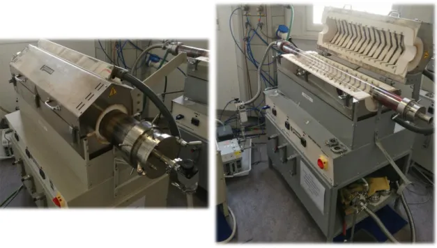
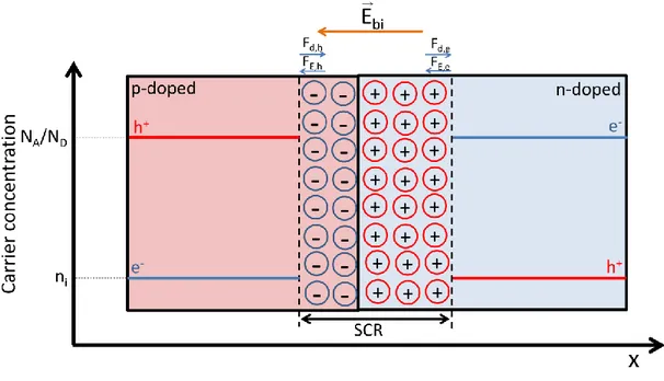
Chapter 1Figure 1. Left: World GDP vs World energy consumption. Right: Growth rate of the world GDP and world energy demand. Sources: World energy consumption extracted from BP’s Statistical Review of World Energy - underpinning data, 1965-2016; real world GDP from United States Department of Agriculture 2 Figure 2. World energy consumption by fuel during 2016. Source: [9] and BP’s Statistical Review of World Energy - underpinning data, 1965-2016. ______________________________________________ 3 Figure 3. Average solar irradiance from 1991 to 1993. The blue discs represent the area needed to be covered with PV power generators to meet the world energy demand assuming an 8% energy conversion efficiency. For more details of the origin of the data check source. Source: [19] __________ 5 Figure 4. Band diagram of a semiconductor. VB and CB stand for valence and conduction band, respectively; Eg stands for the energy of the bandgap and hν is the energy of an incident photon, ____ 9 Figure 5. Diagram of a p-n junction. Ebi stands for the built-in electric field, Fd,x and FE,x with x=h,e stands
for the diffusion and electric force acting on holes (h) and on electrons (e). ______________________ 10 Figure 6. Schematic of selective membrane behaviour (top) and charge separation (bottom) of p-doped and n-doped semiconductors. Ec and Ev are the positions of the conduction band minimum and valence
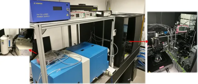
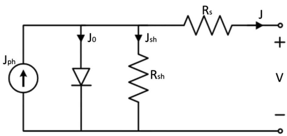
band maximum, respectively. Filled blue circles represent electrons (e-) and hollow red circles holes (h+). The tapered arrows represent the concentrations of the carriers. This figure should only be taken as an illustration and not as a real physical system. ______________________________________________ 11 Figure 7. Basic structure of a p-n junction solar cell. _________________________________________ 13 Figure 8. Characteristic J-V curves of a solar cell represented by equations (6) and (7) (with the sign of the Y axis inverted) and the main parameters used for its description. MTP stands for maximum theoretical power point. _______________________________________________________________ 14 Figure 9. Equivalent circuit of a solar cell with resistive and shunt losses. Jsh stands for the shunt current
density. _____________________________________________________________________________ 15 Figure 10. Structure of a monocrystalline Si PERL solar cell. Reproduced with permission from [45]. Copyrighted by John Wiley and Sons. _____________________________________________________ 16 Figure 11. Pictures of p-Si (left) and c-Si (right) solar cells. Source: http://www.tindosolar.com.au/learn-more/poly-vs-mono-crystalline/ (Accessed on 12/03/19) _____________________________________ 16 Figure 12. Left: a-Si powered calculator. Right: structure of a single junction a-Si solar cell in superstrate configuration. Sources: pixabay.com (right) and [55] (left). ___________________________________ 18 Figure 13. Structure of a CdTe solar cell. Reproduced with permission from [54]. Copyrighted by Elsevier. ___________________________________________________________________________________ 19 Figure 14. Structure of a CIGS solar cell. Reproduced with permission from [72]. Copyrighted by IOPscience. __________________________________________________________________________ 20 Figure 15. EROI of the main PV technologies. Data sources: [23,24,28]. _________________________ 21 Figure 16. Derivation of kesterite crystal structure from zinc blende and chalcopyrite. Adapted with permission from [89]. Copyrighted by American Physical Society. ______________________________ 22 Figure 17. Standard cell configuration and typical layer thicknesses of kesterite solar cells. _________ 24
xi
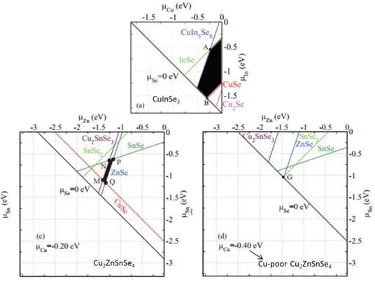
Figure 18. Chemical potential equilibrium diagrams for CuInSe2 (top) and Cu2ZnSnSe4 (bottom). The
black area represents the stable one phase region. Reproduced with permission from [92]. Copyrighted by John Wiley and Sons. _______________________________________________________________ 26 Figure 19. Up-Left: Comparison between the kesterite and stannite crystal structures. Adapted with permission from [89]. Copyrighted by American Physical Society. Up-Right: Ionization levels of intrinsic defects in the band gaps of Cu2ZnSnSe4. The red bars show the acceptor levels and the blue bars show
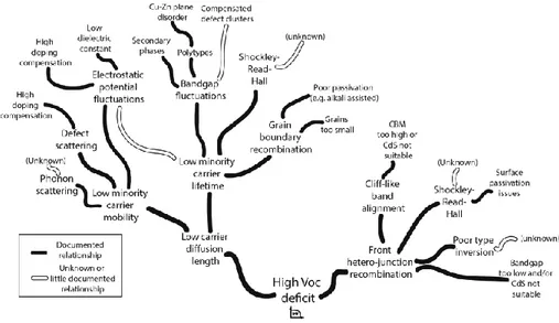
the donor levels, with the initial and final charge states labelled in parentheses. Reproduced with permission from [92]. Copyrighted by John Wiley and Sons. Bottom: bandgap and electrostatic potential fluctuations due to the uneven spatial distribution of defects. Reproduced with permission from [139]. Copyrighted by AIP Publishing. __________________________________________________________ 27 Figure 20. Relationship between different factors affecting the Voc deficit of kesterites. Reproduced with
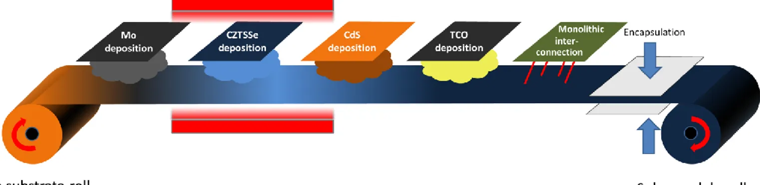
permission from [151]. Copyrighted by Elsevier. ____________________________________________ 28 Figure 21. Sensofar PLu neox confocal microscope.__________________________________________ 35 Figure 22. ZEISS Series Auriga field emission scanning electron microscope. ______________________ 36 Figure 23. Fischerscope XVD X-ray fluorescence analyser. ____________________________________ 38 Figure 24. Constructive interference between elastically scattered secondary X-ray waves fulfilling Bragg's law. _________________________________________________________________________ 39 Figure 25. Bruker D8 Advance X-ray diffraction system. ______________________________________ 40 Figure 26. Raman spectroscopy setup developed at IREC. ____________________________________ 41 Figure 27. UV-vis-NIR spectrophotometer. _________________________________________________ 41 Figure 28. Everbeing four point probe. ____________________________________________________ 42 Figure 29. Keysight E4990A based capacitance-voltage measurement setup. _____________________ 43 Figure 30. J-V analysis setup based on a calibrated Sun 3000 Class AAA solar simulator by Abet Technologies. ________________________________________________________________________ 44 Figure 31. Spectral response system used for EQE measurements. _____________________________ 45 Figure 32. Schematic of DC magnetron sputtering operation. _________________________________ 46 Figure 33. Sputtering systems. __________________________________________________________ 47 Figure 34. Thermal evaporator. __________________________________________________________ 47 Figure 35. Setup for CdS chemical bath deposition. __________________________________________ 48 Figure 36. Graphite box for reactive annealing. _____________________________________________ 49 Figure 37. Hobersal three-zone tubular furnaces. ___________________________________________ 49 Figure 38. Microdiamond scriber. ________________________________________________________ 53 Figure 39. Solar cell with metallic grid and anti-reflective coating. ______________________________ 54 Figure 40. Schematic of a PVD-based kesterite solar module R2R production line. _________________ 55 Figure 41. Left: LWF solar panels integrated in a car. Source:
https://sopraygroup.manufacturer.globalsources.com/si/6008828274640/pdtl/Solar-panel/1062980597/Solar-Panel.htm. Centre: SunnyBag®. Source: https://fr.sunnybag.com. Right: Brunton Solar Roll®. Source: https://www.livefortheoutdoors.com/gear- reviews/accessories/articles/Gear-Reviews/Search-Results/Accessories/Brunton-Solar-Roll-14-2010-solar-panel. _________________________________________________________________________ 56
xii
Figure 42. Alkaline doping strategies studied. ______________________________________________ 59 Figure 43. Homemade frames employed initially for polyimide substrate handling. ________________ 59 Figure 44. Polyimide within frames stuck with Kapton tape to SLG. A reference sample on SLG is shown for comparison. ______________________________________________________________________ 60 Figure 45. CZT precursors on polyimide detached from SLG for selenization. _____________________ 60 Figure 46. Liquid stored in the frames' folds released during ZnO/ITO deposition. _________________ 61 Figure 47. More advanced frame design where polyimide was screwed into a thick piece of stainless steel. _______________________________________________________________________________ 61 Figure 48. Left: bent polyimide substrates after selenization. Right: bent polyimide substrate flattened and stuck onto SLG using Kapton tape. ____________________________________________________ 62 Figure 49. Boxchart of the main solar cell parameters of the samples processed on PI with PAS doping strategy before (solid box) and after (dashed box) hot plate reannealing. ________________________ 63 Figure 50. Boxchart of the main solar cell parameters of the samples fabricated on PI with the PAS doping approach extracted from J-V measurements after LT-PAT. Solid black boxes correspond to the left axes: Efficiency (top) and Voc (bottom). Dashed red boxes correspond to the right axes: FF (top) and
Jsc (bottom). _________________________________________________________________________ 65
Figure 51. J-V (left) and EQE (right) of the best cells fabricated on polyimide with the PAS doping approach. ___________________________________________________________________________ 65 Figure 52. FESEM images of the CZTSe samples fabricated on PI and doped with the PAS approach. Left and middle: top view images of the as-annealed absorbers. Right: cross-sectional images of the full devices. _____________________________________________________________________________ 67 Figure 53. C-V measurements of the record cells of the CZTSe samples fabricated on PI and doped with the PAS approach. ____________________________________________________________________ 68 Figure 54. FESEM top view images of the as-annealed CZTSe absorbers processed at low temperature on SLG. ________________________________________________________________________________ 69 Figure 55. Minimum, maximum and average peak area ratio A(SnSe2)/A(CZTSe) as an estimation of SnSe2
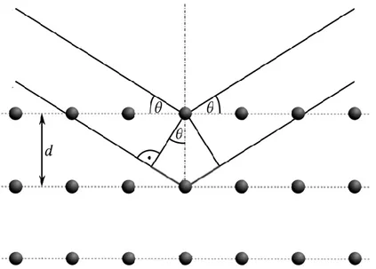
concentration of CZTSe samples synthesized on SLG as a function of annealing temperature. Dashed lines are intended as a visual guide for the reader. Inset: Normalized Raman spectra of the samples. _ 69 Figure 56. Boxchart of the main solar cell parameters of the CZTSe samples processed on SLG at different temperatures before (solid boxes) and after (dashed boxes) hot plate reannealing. ________ 70 Figure 57. FESEM top view images of the as-annealed and etched CZTSe absorbers synthesized on PI with and without Na+Ge doping at different temperatures (batch 1). ___________________________ 72 Figure 58. EDX spectra of the etched surface of the absorbers synthesized on PI with NaF+Ge doping. The red region corresponds to a secondary phase-free region. The black region corresponds to a SnSex
phase cluster. ________________________________________________________________________ 73 Figure 59. Effect of reannealing temperature on the solar cell parameters of a characteristic solar cell of each of the samples. Dashed lines correspond to undoped samples while continuous lines correspond to sample doped with NaF+Ge. ____________________________________________________________ 74 Figure 60. Maximum peak area ratio A(SnSe2)/A(CZTSe) as an estimation of the maximum SnSe2
concentration found in the record cells of the CZTSe samples processed on PI with and without NaF+Ge doping at different temperatures. Inset: Normalized Raman spectra of the samples._______________ 75
xiii
Figure 61. J-V curves of the best performing samples obtained in this work fabricated on SLG (dashed blue line) and on PI with (black) and without (grey) doping at temperatures below 500°C. Inset: table with the main solar cell parameters of the cells. ____________________________________________ 76 Figure 62. Picture of the as-annealed samples showing different bending and contact geometry with the graphite box. ________________________________________________________________________ 79 Figure 63. Voc and efficiency of different cells fabricated in this work as a function of the maximum SnSe2
concentration found in them as estimated by the peak area ratio A(SnSe2)/A(CZTSe) of the Raman
spectra. Dashed lines are intended as a visual guide for the reader. ____________________________ 81 Figure 64. Boxchart of the Rsh of the devices fabricated on SLG at different temperatures before (solid)
and after (dashed) hot plate reannealing extracted from J-V measurements. _____________________ 82 Figure 65. Evolution of Voc and Rsh with reannealing temperature of the record cell from the PI sample
processed at 490°C without doping. ______________________________________________________ 83 Figure 66. BIPV foil Evalon® solar by alwitra. Source: https://alwitra.de/wp-content/uploads/2019/02/alwitra_Evalon_Solar_cSi_GB_2019_01.pdf (accessed on 10/05/19). _____ 86 Figure 67. Solesia® by Creaton. Source: https://www.zi-online.info/en/artikel/zi_2011-10_Sunshiny_days_for_photovoltaics_1265944.html (accessed on 10/05/19). ___________________ 86 Figure 68. Left: Skylights made from spaced opaque modules (left) and semitransparent devices (right) by Onyx Solar. Source: https://www.onyxsolar.com (accessed on 10/05/19). _____________________ 87 Figure 69. Left: Solé PowertileTM. Source: https://cleantechnica.com/files/2010/05/SRS_Tile.jpg (accessed on 10/05/19). Right: Solar roof by Tesla. Source: https://www.solarguide.co.uk/tesla-energy/solar-roof-tiles#/ (accessed on 10/05/19). __________________________________________ 87 Figure 70. Average roughness of the Mo-coated enamelled ceramic substrates. __________________ 91 Figure 71. Pictures of the different Mo-coated enamelled ceramic substrates. ____________________ 92 Figure 72. 3D topographies of the Mo-coated enamelled ceramic substrates. ____________________ 92 Figure 73. Detailed 3D topographies of the Mo-coated ceramic substrates. ______________________ 92 Figure 74. Optical images showing superficial cracks on Mo-coated ceramic substrates with enamels containing more than 8% Na2O. _________________________________________________________ 93
Figure 75. XRD diffractograms of Mo back contact deposited on enamels with different Na2O content. 94
Figure 76. FESEM top view micrographs of Mo back contact deposited on enamels with different Na2O
content. ____________________________________________________________________________ 94 Figure 77. Rsheet of the Mo back contacts deposited on enamels with different Na2O content. _______ 95
Figure 78. J-V (left) and EQE (right) of the best devices fabricated on enamelled ceramic substrates with different Na2O content. ________________________________________________________________ 96
Figure 79. XRD diffractogram of a CZTSe absorber grown on a Mo-coated enamelled ceramic tile (2 wt% Na2O). ______________________________________________________________________________ 97
Figure 80. FESEM micrographs (cross section) of CZTSe solar cells grown on Mo-coated ceramic substrates with enamels containing 2% (top), 8% (middle) and 12% (bottom) Na2O. _______________ 97
Figure 81. Raman spectra of the record device of the 4% Na2O sample (left) together with a low
xiv
Figure 82. Optoelectronic parameters of different solar cells from different samples as a function of the peak area ratio A(SnSe2)/A(CZTSe) obtained from the fitting of Raman spectra. The dashed red lines are
only intended as a visual guide for the reader. _____________________________________________ 99 Figure 83. 3D topographies and Na2O content of the new batch of enamelled ceramic substrates. __ 101
Figure 84. Voc of the top 5 devices found on each substrate. _________________________________ 102
Figure 85. TOF-SIMS depth profile of low and medium Na2O content enamelled ceramic substrates. A
profile corresponding to one of the record devices fabricated in IREC on SLG (not in this work) is also shown for comparison. _______________________________________________________________ 102 Figure 86. J-V curves of the record devices obtained on SLG and 6.6% Na2O enamelled ceramic substrate. Inset: EQE curves of the same devices. __________________________________________ 104 Figure 87. Schematic of albedo light reaching the front and rear sides of a bifacial solar panel in a rooftop installation. __________________________________________________________________ 106 Figure 88. Schematic of light absorption and transmission of different concepts of semi-transparent solar cells. ______________________________________________________________________________ 107 Figure 89. Band diagram of TMO/c-Si before junction (a) and for junctions with n-type (b) and p-type (c) c-Si. The band positions of Si and MoO3 were taken from [297]. The position of the Fermi levels is
arbitrary. __________________________________________________________________________ 110 Figure 90. Total transmittance before (solid line) and after (dashed line) selenization of the SLG/FTO substrates coated with 5, 10 and 20 nm of (a) MoO3, (b) V2O5, (c) TiO2, (d) MoO2, (e) NiO, (f) Co3O4 (g)
CuO. (h) Total transmittance of as deposited TMOs (20 nm) (without the effect of the substrate). ___ 116 Figure 91. Optical band gap of the different TMOs (ordered from lowest to highest) as obtained from the transmittance spectra shown in Figure 91 (h) for 20 nm (squares), 40 nm (circles) and 80 nm (tringles) thicknesses. Inset: logarithmic decrease of the bandgap of MoO3 with the increasing thickness. ____ 117
Figure 92. J-V curves of the record CZTSe devices obtained with each SLG/FTO/TMO substrate configuration. In some cases, the dark J-V curves are also shown as dashed lines. ________________ 120 Figure 93. J-V curves of the record CZTSe devices obtained with each SLG/FTO/TMO/Mo:Na substrate configuration. _______________________________________________________________________ 122 Figure 94. Boxchart of the main solar cell parameters of the devices fabricated on the different substrate configurations. ______________________________________________________________________ 124 Figure 95. EQE of the record devices obtained with in the thickness screening. __________________ 126 Figure 96. Total transmittance before (solid line) and after (dashed line) selenization of the best performing substrate configurations. ____________________________________________________ 127 Figure 97. Cross-sectional FE-SEM micrographs of the best performing CZTSe, CZTS and CZTSSe devices on the different substrate configurations. ________________________________________________ 130 Figure 98. Raman spectra of the CZTSe, CZTSSe and CZTS devices fabricated on the different substrate configurations. The measurements were carried out at the front surface (continuous lines) and the back surface (dotted lines) employing λex = 785 nm. ____________________________________________ 131
Figure 99. FWHM of the 195 cm-1 (CZTSe), 335 cm-1 (CZTSSe) and 337 cm-1 (CZTS) peaks extracted from Lorentzian fittings. The S/(S+Se) ratios calculated with a similar method to that described in [323] are shown for CZTSSe. ___________________________________________________________________ 132 Figure 100. TOF-SIMS spectra of the best CZTSe (a), CZTS (c) and CZTSSe (d) performing devices fabricated on SLG/FTO/TiO2/Mo:Na, SLG/FTO/Mo:Na and SLG/FTO/V2O5/Mo:Na, respectively, obtained
xv
from the Cs+ signal. b) CZTSe spectrum obtained from the O2+ signal. Elements displayed: Cu (blue), Sn
(red), S/Se (dark yellow), V/Ti (orange), Na (purple), Mo (dark grey), Cd (yellow) and O (blue). The boundaries between the different layers shown in the spectra are only intended as a visual guide for the reader. ____________________________________________________________________________ 133 Figure 101. Transmittance spectra of the finished devices. ___________________________________ 134 Figure 102. Band diagrams of CZTSe, CZTS and FTO. Data sources: CZTSe and CZTS [330]; FTO [331]. _ 135 Figure 103. Reference and record J-V curves obtained for CZTSe, CZTS and CZTSSe devices fabricated on SLG/FTO. ___________________________________________________________________________ 141
xvi
List of tables
Table 1. Reserves and depletion year of fossil fuels. Source: BP’s Statistical Review of World Energy - underpinning data, 1965-2016 and [11].*Assuming 2016’s proven reserves and consumption. †Assuming a 28% linear increase of consumption for every fossil fuel from 2016 to 2040. ‡Assuming estimated 2040’s remaining reserves and consumption. _______________________________________________ 4 Table 2. Embedded energy of module fabrication of the main PV technologies. Data source: [28]. ____ 21 Table 3. Selection of the best solar cells reported for different kesterite compounds and synthesis routes. The best devices of each compound are highlighted in bold. The ‘/’ symbol in the ‘Precursor Type’ column indicates that the precursor is composed by different stacked layers. In the ‘Annealing Technique’ column HP stands for Hot Plate, RTP for Rapid Thermal Processing and TF for Tubular Furnace. The ‘-‘ symbol is used when no information is available. *Homemade halogen lamp-based
furnace. ____________________________________________________________________________ 24
Table 4. Comparison of the record CIGS and CZTSSe devices. __________________________________ 25 Table 5. Main effects of Na in CZTSSe absorbers reported in the literature. ______________________ 29 Table 6. Typical sputtering deposition parameters for Mo back contacts. P stands for deposition power, pB for the minimum base vacuum before deposition and p to the Ar pressure employed during
deposition. __________________________________________________________________________ 50 Table 7. Typical sputtering deposition parameters for the metallic precursor stack. P stands for deposition power, pB for the minimum base vacuum before deposition and p to the Ar pressure
employed during deposition. ___________________________________________________________ 51 Table 8. Reactive annealing parameters for kesterite absorber synthesis. ________________________ 52 Table 9. Typical sputtering deposition parameters for ZnO and ITO. P stands for deposition power, pB for
the minimum base vacuum before deposition and p to the Ar+O2 pressure employed during deposition.
___________________________________________________________________________________ 53 Table 10. Main properties of Upilex 50S polyimide foils. Source: http://www.upilex.jp/catalog/pdf/upilex_s_e.pdf?20190220. _________________________________ 57 Table 11. Parameters of the record cells of the CZTSe devices fabricated on PI with different doping strategies extracted from J-V measurements. ______________________________________________ 64 Table 12. Average and standard deviation (in brackets) of the main solar cell parameters of the CZTSe devices fabricated on SLG at different temperatures extracted from J-V measurements. The last two rows show the parameters of a cell from the 490°C sample containing SnSe2 and from the SnSe2-free
record cell. AF stands for “As-fabricated” and AR stands for “After hot plate reannealing”. _________ 71 Table 13. Main solar cell parameters of the CZTSe record devices fabricated on PI with and without NaF+Ge doping at different temperatures (batch 2) extracted from J-V measurements. ____________ 75 Table 14. Rs and Rsh of the record cells fabricated with PAS doping. _____________________________ 77
Table 15. Composition and main properties of ecologic ceramic substrates. ______________________ 89 Table 16. Solar cell parameters of the best devices prepared on the enamelled ceramic substrates with different Na2O composition. ____________________________________________________________ 96
Table 17. Solar cell parameters of the best devices prepared on the new batch of enamelled ceramic substrates. _________________________________________________________________________ 101
xvii
Table 18. Main optoelectronic properties of the TMOs employed in this work. __________________ 112 Table 19. Average transmittance of the different TMOs deposited on quartz without the effect of the substrate. Values calculated from Figure 91 (h). ___________________________________________ 115 Table 20. Average transmittance of the SLG/FTO substrates coated with 5, 10 and 20 nm of the different TMOs calculated from Figure 91 (a-g). The values in red were measured after submitting the substrates to a selenization annealing process. _____________________________________________________ 118 Table 21. Solar cell parameters of the record devices obtained with each SLG/FTO/TMO (left) and SLG/FTO/TMO/Mo:Na (right) substrate configuration. The rows in bold correspond to devices with efficiencies above those of the reference TMO-free substrates. ______________________________ 121 Table 22. Optoelectronic parameters of the record devices obtained with each substrate configuration. The rows in bold correspond to the best configuration obtained with each TMO. ________________ 125 Table 23. Average transmittance values of the best performing substrate configurations. The values in red were measured after submitting the substrates to an annealing process. Values calculated from Figure 96. __________________________________________________________________________ 127 Table 24. Optoelectronic parameters of the record devices obtained with each substrate configuration and kesterite absorber. The rows in bold correspond to the best configuration obtained for each absorber. __________________________________________________________________________ 129 Table 25. Main advantages (green) and limitations (red) of the substrates studied. _______________ 142
1
1. Introduction
1.1 Energy supply in a growth-addicted financial
system: what is the role of photovoltaics in all
this?
1.1.1 The threat of fossil-fuel dependence: the hidden link between
economy, growth, complexity and energy
Although most people tend to ignore it, either because they do not know or want to think about it, human civilization and our current model of society might be at the edge of collapse. The main reason for this is that the global financial system on which our current civilization is founded has developed in such a way that it requires continuous and sustained growth in order to function correctly and provide “stability” [1–3]. The most clear aspect of its growth-dependency is the use of debt as the motor driving the economy: banks, companies and governments create different types of debt with interest rates that can only be repaid in the future when the global economy has grown [3,4]. But, what is growth, where does it come from and why is it threatening for our society?
It is necessary to start this brief analysis by understanding that our financial system and even our civilization behaves and can be accurately modelled as a complex adaptive system (CAS), i.e. a system comprised by individual parts that are able to adapt as a whole to generate a collective shift in its internal behaviour in order to prolong its existence [2,3,5,6]. Living organisms and ecosystems are typical examples of CASs. In this context, growth can be defined and understood as an increase in the complexity of the system. The complexity of a CAS is represented by its size, the distinctiveness of its constituent parts, the diversity of specialised roles that it incorporates, the information exchange between its parts and the self-organising mechanisms that convert these into a coherent, functioning whole [3,7]. In the case of human civilization, we commonly identify the increase of complexity as “progress”: rise of world population, globalised economy, advances in science and technology, high degree of interconnection through the development of transport and telecommunication infrastructures, etc.
The evolution of every complex system found in nature, including our global economy and civilization, is subjected to the laws of thermodynamics [2,3,5]. In particular, the second law of thermodynamics states that physical systems, such as CASs, tend to dissipate energy (in the form of heat) and increase their entropy until reaching equilibrium with their surroundings. Therefore, growth or increased complexity (which denotes ordered or low entropy states) goes against the natural thermodynamic flow toward randomness [6]. However, CASs are open systems that are able to overcome thermodynamic decay by using low entropy energy and transforming it into useful work before dissipating it in the form of heat to their surroundings and, this way, maintain and even increase their complexity [2,3,5,6]. In other words, CASs can
![Table 2. Embedded energy of module fabrication of the main PV technologies. Data source: [28]](https://thumb-eu.123doks.com/thumbv2/123dokorg/4436697.29857/52.892.131.762.540.907/table-embedded-energy-module-fabrication-technologies-data-source.webp)