UNIVERSITA’ DELLA CALABRIA
Dipartimento di Ingegneria Informatica, Modellistica, Elettronica e Sistemistica
Dottorato di Ricerca in
Information and Communication Engineering For Pervasive Intelligent Environments
CICLO XXIX
mm-Wave Antennas For Satellite And Mobile Communications
Settore Scientifico Disciplinare Campi Elettromagnetici
Coordinatore: Ch.mo Prof. Felice Crupi
Firma _____________________________
Supervisore/Tutor: Ch.mo Prof. Giandomenico Amendola Firma______________________
Dottorando: Dott. Francesco Greco
List of figures 4
List of Acronyms 10
Abstract 11
1. Antenna Needs for future Applications at Millimeter Waves 13
1.1. Satcom on The Move (K/Ka- band) 14
1.2. High speed Millimeter Waves link 15
1.3. Radar automotive applications 17
2. A Dual Band, Dual Polarized array for Ka band Satcom on the Move terminals 19
2.1. State of the art 19
2.2. Dual-Bands, Dual-Polarized array antenna 21
2.2.1. Radiating element 21
2.2.2. Antenna array 25
2.2.3. Measurements 30
3. Cylindrical Reflector Antenna for wireless communication systems 36
3.1. State of the Art 36
3.2. Cylindrical Reflector antenna 40
3.2.1. Parallel Plate 41
3.2.2. Hat Feed 43
3.2.2.1. General considerations 43
3.2.2.2. The hat feed for a cylindrical reflector – Theory 47 3.2.2.3. Single and Dual and hat feed for a cylindrical reflector 55
3.2.2.4. Gaussian Vertex plate 61
3.2.3. Cylindrical reflector realization and measurements 62
4.1. State of the art 75
4.2. Segmented reflectarray 76
4.3. Simulated and measured results 83
5. Transmitarray antenna for Radar Automotive applications 88
5.1. Transmitarray theoretical model 88
5.2. State of the art 89
5.2.1. Transmitarray antenna configurations 89
5.2.2. Discrete Lens Arrays 90
5.2.3. Antenna Filer Antenna (AFA) 90
5.2.4. Multilayer Antenna Filter Antenna (MAFA) 91
5.2.5. Frequency Selective Surface (FSS) 93
5.3. Transmitarray antenna for radar automotive 94
5.3.1. Transmitarray efficiency performance 101
5.3.2. Designing procedure of the transmitarray antenna 106
Conclusions and future work 114
List of figures
Fig. 2.1 - Dual-Bands, Dual-polarized radiating element ... Fig. 2.2 - Dual band single element geometry ...
Fig. 2.3 - Simulated S parameters and Gain of the Rx radiator ... 24
Fig. 2.4 - Simulated S parameters and Gain of the Tx radiator ... 24
Fig. 2.5 - Dual bands, Dual-polarized array antenna ... Fig. 2.6 - Stack-Up of the array antenna ... 27
Fig. 2.7 - Section view of the Dual Band, Dual polarized array antenna ... 27
Fig. 2.8 - Simulated S-parameters in Rx band of the array configuration ... 28
Fig. 2.9 - Simulated S-parameters in Tx band of the array configuration ... 28
Fig. 2.10 - Radiation pattern at 20GHz ... 29
Fig. 2.11 - Radiation pattern at 30GHz ... 29
Fig. 2.12 - RHCP radiation pattern at frequency of 20GHz ... 30
Fig. 2.13 - RHCP radiation pattern at frequency of 30GHz ... 30
Fig. 2.14 - Bottom view of the antenna ... 31
Fig. 2.15 - Top view of the antenna ... 31
Fig. 2.16 - Antenna with MMPX to K transition ... 31
Fig. 2.17 - Gain of the horizontal polarization in Rx band ... 33
Fig. 2.18 - Gain of the vertical polarization in Rx band ... 33
Fig. 2.19 - Vertical polarization in Rx band ... 33
Fig. 2.20 - Horizontal polarization in Rx band ... 34
Fig. 2.21 - Gain of the horizontal polarization in Tx band ... 34
Fig. 2.22 - S parameters of the horizontal polarization in Tx band ... 35
Fig. 3.1 - 5G hybrid radio access architecture with a macro-cell providing microwaves access, mmW small cells and mmW backhaul. ... 37 Fig. 3.2 Structure of Cylidrical Reflector ...
Fig. 3.3 - Parallel plate structure ... 41
Fig. 3.4 Field distribution inside the PPW ... 42
Fig. 3.5 - Radiation Pattern of the PPW ... 42
Fig. 3.6 - Profile of the Hat Feed with its three main parts ... 43
Fig. 3.7 - Hard and soft surface structure ... 44
Fig. 3.8 - Ray-fixed coordinate system ... 45
Fig. 3.9 - Transverse corrugations ... 46
Fig. 3.10 - Infinite corrugated ground plane ... Fig. 3.11 - Radiation and surface wave regions in the k0 L-β0 L plane ... 54
Fig. 3.12 - Radiation and surface wave regions in the k0L-βnL diagram ... 55
Fig. 3.13 - Dual band Hat feed ... 56
Fig. 3.14 - Hat Feed with a single corrugation ... 56
Fig. 3.15 - Reflection coefficient in Rx-band ... 57
Fig. 3.16 - Reflection coefficient in Tx-band ... 57
Fig. 3.17 - Simulated radiation pattern of the Hat Feed at the 40GHz and 60GHz ... 58
Fig. 3.18 - Input impedance of the single corrugation ... 59
Fig. 3.19 - Hat Feed with a dual corrugations ... Fig. 3.20 - Input impedance of the dual corrugation at the optimal point ... 60
Fig. 3.21 - Simulated radiation pattern of the hat feed with two corrugations at the centre frequency of the two bands ... 61
Fig. 3.22 - Gaussian vertex plate in a reflector antenna ... 62
Fig. 3.23 - Simulated structure of the overall antenna in Q-V bands ... 63
Fig. 3.24 -Frontal view of the overall antenna in Q-V bands ... 63
Fig. 3.25 - Realized prototype antenna in Ka band ... Fig. 3.26 - Top view of the realized antenna in Ka band ... 64
Fig. 3.27 - Feeding structure of the realized antenna ... 65
Fig. 3.28 - Measured S11 (Rx band) ... 66
Fig. 3.29 - Measured S11 (Tx band) ... 66
Fig. 3.30 - Comparison between simulated and measured results (Plane E) at 19GHz ... 67
Fig. 3.31 - Comparison between simulated and measured results (Plane H) at 19GHz ... 67
Fig. 3.32 - Comparison between simulated and measured results (Plane H) at 20GHz ... 68
Fig. 3.33 - Comparison between simulated and measured results (Plane E) at 20GHz ... 68
Fig. 3.34 - Comparison between simulated and measured results (Plane H) at 21GHz ... 69
Fig. 3.35 - Comparison between simulated and measured results (Plane E) at 21GHz ... 69
Fig. 3.36 - Comparison between simulated and measured results (Plane E) at 29GHz ... 70
Fig. 3.37 - Comparison between simulated and measured results (Plane E) at 30GHz ... 70
Fig. 3.38 - Comparison between simulated and measured results (Plane E) at 31GHz ... 71
Fig. 3.39 -Comparison between simulated and measured gain (Rx Band) ... 71
Fig. 3.40 - Measured gain (Tx Band) ... 72
Fig. 3.41 - Mask Comparison ... 73
Fig. 3.42 - Radiation pattern of the terminal along the plane 45° at 29GHz ... 73
Fig. 3.44 - Radiation pattern of the terminal along the plane 45° at 31GHz ... 74
Fig. 4.1(a) - Segmented Reflectarray ... 77
Fig. 4.2 - Boundary conditions for the simulations of the unit cell of the reflectarray ... 78
Fig. 4.3 - Amplitude response of the reflection signal of the unit cell ... 79
Fig. 4.4 - Phase response of the reflection signal of the unit cell... 79
Fig. 4.5 - Schematic structure of the reflectarray ... 80
Fig. 4.6 - Efficiency of the reflectarray related to the inter-element spacing ... 81
Fig. 4.7 - Efficiency of the reflectarray(b) considering different radiation pattern (a) ... Fig. 4.8 - Efficiency of Reflectarray related to number of segment ... 82
Fig. 4.9 - S-parameters of Segmented Reflectarray ... 84
Fig. 4.10 - Comparison of phase distribution along the aperture in the Parabolic Reflector and Segmented Reflectarray ... 84
Fig. 4.11 - Comparison of field distribution along the aperture in the Parabolic Reflector and Segmented Reflectarray ... 85
Fig. 4.12 - Comparison of gain performance along the band of interest in the Parabolic Reflector and Segmented Reflectarray ... 85
Fig. 4.13 - Section view of the segmented reflectarray ... 86
Fig. 4.14 - Comparison between measured and simulated radiation pattern at center band (20GHz) ... 86
Fig. 5.1 - Theoretical structure of Transmitarray antenna [20] ... 88
Fig. 5.2 - An antenna-filter-antenna array composed of patch antennas [25] ... 91
Fig. 5.3 - MAFA structure [26] ... 92
Fig. 5.4 - Typical FSS types and their frequency response characteristics [27] 93 Fig. 5.5 - Chip on board integration [28] ... 94
Fig. 5.6 - Lens antenna on chip [29] ... 95
Fig. 5.7 – Concept of transmitarray integrations in package ... 95
Fig. 5.8 - Transmitarray structure ... Fig. 5.9 - Ring cell classification around the transmitarray central point ... 98
Fig. 5.10 - Field distribution in the transmitarray ... Fig. 5.11 - Schematic view and power budget of a transmitarray ... 100
Fig. 5.12 - Graphical view of Spillover Efficiency. ... 101
Fig. 5.13 - Results for the study of different values of the parameter F/D ... Fig. 5.14 - Radiation pattern with the model cosn θ ... Fig. 5.15 - Results obtained for directivity and spillover efficiency, depending of n ... Fig. 5.16 - Impact of element spacing in the directivity ... Fig. 5.17 - Scheme of the unit cell of transmitarray antenna ... 106
Fig. 5.18 - Transmission coefficient as a function of patch side: Amplitude and Phase ... 107
Fig. 5.19 - Footprint of the M-QFN80T.5 package ... Fig. 5.20 - A generic scheme of the chosen transmitarray ... 108
Fig. 5.21 - Section view of the transmitarray at 77GHz ... 108
Fig. 5.22 - Integration between QFN package and patch antenna ... 109
Fig. 5.23 - Surface wave effect on the radiation pattern of the patch at 77GHz ... 110
Fig. 5.24 - Surface wave effect on the radiation pattern of the Transmitarray at 77GHz ... 110
Fig. 5.25 - Structure of the Electromagnetic Band Gap ... 111
Fig. 5.26 - Patch antenna with Mushroom EBG ... 111
Fig. 5.28 - Transmitarray antenna with a QFN package at 77GHz ... 112 Fig. 5.29 - Radiation pattern of the Tx array feeding by patch antenna with EBG at 77GHz ... 113
List of Acronyms
Fixed Satellite Service FSS
Mobile Satellite Service MSS
Broadcasting Mobile Satellite Service Satellite Service BSS Earth Exploration Satellite Service ESS
Space Research Service SRS
Space Operation Service SOS
Radiodetermination Satellite Service RSS
Inter-Satellite Service ISS
Amateur Satellite Service ASS
International Telecomunication Union ITU
Direct-to-Home DTH
Global Positioning System GPS
Maximum usable frequency MUF
Optimum Working Frequency OWF
Low-Earth-Orbit LEO
Medium-Earth-Orbit MEO
Geostationary-Earth-Orbit GEO
Satcom-On-the-Move SOTM
Carrier-to-noise-ratio CI
Adjacent Satellete Interference ASI Equivalent Isotropic Radiated Power EIRP
Local Area Network LAN
Abstract
Ever growing demands for higher data rate and bandwidth are pushing wireless applications to millimetre-wave band (3-300GHz), where sufficient bandwidth is available and high performance can be achieved without using complex modulation systems. In addition to Telecom applications, millimetre-wave bands has enabled novel short range and long range radar sensors for automotive as well as high resolution imaging systems for medical and security. The major obstacle for the wide deployment of commercial wireless and radar systems in this frequency range is the high cost of the overall system. The main object of this work is to investigate and to develop different type of antenna that could be applied in satellite communications, in the future fifth generation of mobile networks and on radar automotive systems. In particular, in the present thesis, four antennas have been developed.
A dual band dual polarized antenna array for Satcom-On-The-Move application that gives the possibility to obtain a fixed beam on the frequency range 19-21GHz (Rx band) and 29-31GHz (Tx band). This structure could be used in association with a fully mechanical pointing system.
A Reflector terminal in the Q/V bands that could be use on the backhaul point of the 5G future architecture. A Ka band scaled version of the antenna has been realized and measured proving that it can be a valid solution for compact earth terminals. A novel reflectarray with potential applications in both satellite communications and high speed point-to-point radio links.
Finally, a 77GHz transmit-array antenna mounted on a QFN package. This kind structure, due to the compact dimensions, could be represent a possible solution for automotive radar system.
1.
Antenna Needs for future Applications at
Millimeter Waves
The main factor that influences the adoption of frequency bands up to mm-wave is the available spectrum. In fact, the always increasing volume of data to be exchanged calls for larger and larger bandwidth which are available only in high frequency ranges. For this reason the spectrum of frequency called millimetre wave (>30GHZ) is currently being studied and used in new, high performance data links. The list of applications which rely on millimetre wave band is already long. Satellite communications at K/Ka occupies from 17.7GHz to 21.2GHz in RX and from 27.5GHz to 31GHz in TX mode. Band around 40GHz is typically used for cellular backhaul and long-distance links, providing data rates that are in the range of several hundred Mb/s. Gb/s data rates, have been realized at 60GHz, 70GHz an 80GHz in system currently available. Other than communications applications, millimetre waves have found applications in automotive radars that operate in the band 76GHz-77GHz for long range radars while the band 77GHz-81GHz is allocated to short-range radar.
In this chapter is presented a brief description of the applications for which the antennas presented in the following parts of this thesis have been designed. The description, rather than exhaustive, focus on a few aspects that are considered critical in the design phase.
1.1.
Satcom on The Move (K/Ka- band)
In addition to Ku-band, Ka-band is nowadays available in the following frequency ranges: 27.5 to 31.0GHz uplink and 17.7 to 21 GHz downlink For this band, new design solutions and technologies, adopted by terminal equipment manufacturers, allowed the development of more spectrally efficient, ultra-small terminals that can provide broadband. This is true for both mobile (Satcom On The Move) and fixed applications. The design of antennas for satellite communications have to satisfy several requirements. In general, they have to provide TX and RX operations, support circular polarization (if required) and to be efficient to satisfy the requirements on the radiated EIRP and G/T. Another important specification is relevant to the unwanted interference towards adjacent satellites (ASI-Adjacent Satellite Interference), which is expressed in terms of power spectral density masks within which the power radiated by the antenna has to stay.
Technical and operational characteristics for Satcom on the Move are different from those of fixed satellite communications. One of the most important, is the small antenna size that is necessary to operate from a moving vehicle, aircraft or vessels. A small size is mandatory because the antenna has to be mounted on a tracking system that is required to maintain accurate pointing to the target satellite at all times. However, as vehicles move, there is always a probability that antenna-pointing errors may occur for small fractions of time, thus leading to an increase of interference toward other co-frequency neighbouring satellites or other radio-systems. This possibility requires that systems have to be designed and operated rigorously to minimize interference and comply with established regulations. As it was already stated, the reduction of interfering signals towards adjacent satellite is a fundamental issue. Early satellite communications systems
utilized rather large earth terminal antennas with very high discrimination to and from adjacent satellite. SOTM terminal are so small that they have exactly the opposite effect. In fact, the small aperture size offers relatively large beam-width towards the satellite of interest and simultaneously radiate a significant amount of energy towards adjacent satellite [1].
The need of compact antenna is not limited to SOTM applications. In fact, there are applications calling for fixed earth terminals with a reduced size. This is the case of man transportable terminal used in defence and security applications which are normally carried by a single operator in difficult conditions. The design of such antennas shares many difficulties with the design of SOTM radiators. In particular, as in the SOTM case, they have to provide dual band operations, comply with radiation masks to avoid interference on the adjacent satellites and to be efficient to satisfy the requirements on the radiated EIRP and G/T.
In the following chapters two antennas will be presented that have the potential to satisfy the requirements discussed previously: a printed antenna with dual band (19-21GHz and 29-31GHz) capabilities for TX/RX operations and two polarizations per band; a compact low profile reflector TX/RX antenna which complies with power density masks. As a further study the potential use of a reflectarray based antenna has been evaluated.
1.2.
High speed Millimeter Waves link
The problem of providing the EIRP calculated by link budgets and, at the same time to radiate into the prescribed Power Density Masks, is not limited to satellite communications but has to be faced also in the design of antennas for point-to-point terrestrial radio link. The availability of high- speed radio links is fundamental
for the operation of the current mobile networks and it will be even more important in the future systems (5g). In fact, the current fourth generation for mobile communications already uses advanced technology, such as orthogonal frequency division multiplexing (OFDM) or multiple input multiple output (MIMO), in order to achieve spectral efficiency close to theoretical limits in terms of bits per second per Hertz per cell [2]. One possibility to increase the capacity per geographic area is to deploy many smaller cells such as femtocells and heterogeneous networks. However, because capacity can only scale linearly with the number of cells, small cells alone will not be able to meet the capacity required to accommodate an increase of orders of magnitude in mobile data traffic as required by new applications. In this case, the only option is to recur to millimetre waves base stations (MMB). In order to ensure good coverage base stations at millimetre waves need to be deployed with higher density than macro-cellular base stations. The transmission and reception in an MMB system are based on narrow beams, which suppress the interference from neighbouring MMBs and extend the range of an MMB link. This allows significant overlap of coverage among neighbouring base stations. Unlike cellular systems that partition the geographic area into cells with each cell served by one or a few base stations, the MMBs form a grid with a large number of nodes to which a mobile station can attach. This possible solution has the advantage to eliminate the problem of poor link quality at the cell edge that is inherent in cellular system and enables high-quality equal grade of service. However, the main disadvantages is that MMB have to be networked between them and to the overall system with high speed links. To avoid the considerable costs of a system based on optical fibers, a network of point-to-point radio links may prove an effective solution. For this reason, it is possible to forecast that a growing number of high speed point to
point links will be deployed in the future. This will push more attention on low cost, efficient mmw antennas able to comply with regulations on power density masks. In this thesis, the compact antenna design already mentioned in the previous section is adopted to design a Q/V band antenna for high speed point-to-point link.
1.3.
Radar automotive applications
The focal point of the next generation of wireless and sensing systems is to obtain a reconfigurable antenna beam forming. High gain pencil-beam or multi-beam synthesis is essential to many systems including satellite communications, cellular base stations, remote sensing, point-to-point terrestrial links, deep-space communication links and radars automotive. Focusing the attention on radar automotive applications, this sector will reach an inflection point which the control of vehicles, in a not too distance future, radars will be used in lane, blind spot detection, adaptive cruise control, collision warning and pedestrian detection. It is projected that by the year 2020, traffic congestion in many cities around the world will reach unresolvable levels unless vehicles incorporate autonomous control to coordinate the movements for optimum traffic flow. The frequency band of 77GHz has proven to be attractive of automotive radar-based safety applications, including for adaptive cruise control, blind-spot detection, emergency braking, forward collision warning and rear collision protection are some automotive applications, which are based on high performance radar sensors. A conventional approach to realize beam scanning radar sensor is to use phased array antennas. They provide electronic flexibility in exciting the elements, allowing for reconfiguration and scanning of the beam pattern in real
time. Although phased array antennas are capable of providing a wide beam steering angle, the disadvantage is that each array element needs to be connected to a dedicate transceiver module. Furthermore, phased arrays diminish in efficiency at millimetre-wave frequencies due to use of transmission-line feeding networks which become increasingly loss at high frequencies and also phased arrays have the drawbacks of high costs and bulky structure.
In the last chapter of this thesis is presented the design of a highly integrated transmitarray antenna at 77GHz which is conceived to give a low cost solution for the new generation of automotive radars.
2.
A Dual Band, Dual Polarized array for Ka band
Satcom on the Move terminals
2.1.
State of the art
During the recent years, a large numbers of terminals for Satcom-On the Move applications were studied and produced. This kind of terminals must to be able to operate in regions with undeveloped infrastructure, distant from big cities, but still in areas of satellites services. Key element of the SOTM terminal is antenna which should have to satisfy the following restrictions [3] :
A narrow beam to receive/transmit wideband signals from/to the satellite Satellite tracking capabilities for SOTM operation
Low sidelobes meeting ITU Rec Low profile and streamline design Small size and weight
Low power consumption High reliability
In order to satisfy all of these features, three classes of SOTM antennas can be specified: antennas with two-dimensional mechanical scanning; antennas with two-dimensional electrical scanning and systems with combined scanning, where the scanning is electrical in the elevations plane and it is mechanical in the azimuth plane. The solution currently available is the fully mechanical one, even if there are examples of the other kind of antennas reported in literature. The direct line-of-sight between the earth terminal and the satellite requires the
terminal antenna to see from horizon to overhead in elevation and 360° in azimuth angle, with total hemispherical coverage. This is realized by mounting the antenna on a moveable platform. The pointing mechanism has also stringent requirements as well because, in spite of constant vibrating, pitching, rolling and yawing the Mobile SatCom antenna’s narrow radiation beam must be pointed accurately to satellite. Furthermore, mobile antenna have to satisfy the requirements of robustness, easy installation and reasonable cost. While antennas installed on ships or large vessels do not need too much space, terminal mounted on terrestrial vehicles and aircraft need smaller and aerodynamic antenna.
Other than the challenges posed by mechanical steering which requires radiator as small and light as possible, the electrical design is cumbersome by itself. In fact, to reduce its size, the antenna has to support TX and RX operations on a single radiating surface, to provide polarization switching and have good efficiency.
In the following is presented the design of a printed antenna array which operates on the frequency bands allocated to K/Ka band satellite communications (RX:19.1GHz-20.1GHz-TX:29GHz-31GHz) able to support polarization switching. The main challenges are to design a self diplexing radiating elements, able to cover both TX and RX bands, and to identify a lattice which can accommodate the dual band elements while avoiding the onset of grating lobes
2.2.
Dual-Bands, Dual-Polarized array antenna
The design of an array able to integrate both Tx and Rx operation in a single aperture is difficult to realize but it is essential. Two solutions may be take into account: array of elements with a bandwidth large enough to cover both Tx and Rx or a arrays od dual-band elements. The first solution has been largely explored [4]. For example, arrays of tightly coupled dipoles with ultra wideband performance have been recently studied [5] for Ku-band SOTM showing excellent scanning behaviour in a wide angular range. However, this approach has two main problems which surfaces even in the case of fixed beam antennas which are not designed for electronic beam steering. The reduced cell size results in an increased number of elements and, consequently, in a excessively complex Beam Forming Network. Secondly, an element covering bot TX and RX bands would need some mechanism to isolate the two bands which would make more complex the design. To avoid these problems, a configuration of radiating element based on coaxial printed rings was chosen [6]. This kind of element is preferred because it is naturally self diplexing, i.e. it provides a good TX/RX isolation while showing enough bandwidth and good efficiency. Also it permits the design of independent TX and RX BFN which can be realized at different levels of the stack up so ensuring good isolation.
2.2.1. Radiating element
The radiating element is designed to have dual-band operations, 19-21GHz (Rx band) and 29-31GHz (Tx band) and it is shown in Fig. 2.1 and in Fig. 2.2. It is composed of two nested radiators and it is based on the design presented in [6]. The outer radiator is a coaxial structure formed by a cage of metalized via holes
and it operates on the Rx band. The inner radiator is actually a circular waveguide operating in Tx band. The ring of via-holes forms a conducting wall that helps to minimize the impact of mutual coupling effects. The two radiators are fed with different techniques. In the Rx band a stripline feed is used, where strips enter into the radiator between adjacent via-holes. Dual polarization is obtained placing the feeding network at different levels to obtain a good isolation between the two polarizations. As it can be seen, two feed are used for each line to enforce linear polarization and to improve isolation. The inner radiator is fed with two microstrip on the lower ground plane coupled to two orthogonal slots placed in T configuration. Notice that the Rx feeding lines for the two polarizations are physically isolated between them and from the Tx feeding lines. The overall thickness of the antenna is about 2.5mm.
Outer ring Inner Ring Thickness Dual Band Dual
Polarized antenna
8mm 3.5mm 2.56mm
Tab 2.1 – Characteristics of the antenna
The Rx radiator has a gain of approximately 7dBi and a flat behaviour on the overall band of interest, while the gain of the Tx radiator is 6dBi. This higher value of the gain in Rx band is related to the shorted pin near feeding line that both increase the isolation and gain level. In the figure listed below (Fig. 2.3 and Fig. 2.4) are reported the reflection coefficient and the coupling between Tx and Rx
30GHz radiating element 20GHz radiating element
Shorting pins
Ground with coupled slot
elements. The geometry of both antennas was optimized to obtain a good impedance match to 50Ω in the whole bands without requiring additional matching networks. As it is shown, the two antenna are highly isolated especially in the lower band because at this frequency the inner radiator is in cut-off.
Fig. 2.3 - Simulated S parameters and Gain of the Rx radiator
2.2.2. Antenna array
If the distance of the elements is too large, grating lobes may appear on the radiation pattern of the antenna. As it is known, grating lobes are unwanted radiation peaks pointing at directions not collinear to the main beam, and are related to the element spacing. The well known formula
𝑑 < λ(1 + sin θ)
gives an upper bound to the inter-element distance before grating lobes appear. At θ=0°, the separation d can be large as λ before the onset of the first grating. However, this constraint related to the inter element spacing is theoretical, in fact during the design procedure d<0.9 λ is normally considered as the maximum value that inter element spacing could assume. Considering the present work, the diameter of the outer radiator is 8mm, as reported in Tab. 2.1.This mean that it is not possible to utilize a rectangular lattice array, otherwise grating lobes will appear in the radiation pattern. According to this restriction, a triangle lattice configuration was adopted. Using this configuration, the grating lobes occur when:
𝑑 < 1.15𝜆/(1 + 𝑠𝑖𝑛𝜃)
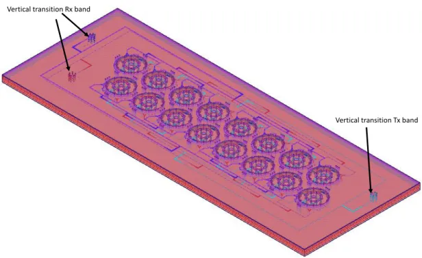
allowing more space to accommodate the radiating elements. In Fig. 2.5 it is shown the array of elements placed in the triangular lattice. Also visible are the BFN which feed independently the dual polarized TX and RX elements
The radiating element were designed in view of their integration in a dual-band dual-polarization array antenna. In Fig. 2.6 a cross sectional view of the array is reported. The array antenna has been designed in order to obtain a good isolation between both different polarizations and different bands. For this reason, during the design of the array structure, it was adopted a different solution for the feeding network of the Tx elements. In particular, one polarization was fed by a microstrip-feeding network on the lower ground plane coupled with the antenna through a slot while the other polarization was fed through a stripline feeding network such as the feeding network of the Rx element. Thanks to this solution, it was possible to isolate all the different source and to realize a 8x2 array antenna (Fig. 2.7). To obtain an easier integration with electronic components in the future, vertical transition were used. In this way all the input were placed on the same layer of the microstrip line (Fig. 2.7).
Fig. 2.6 - Stack-Up of the array antenna
Fig. 2.7 - Section view of the Dual Band, Dual polarized array antenna
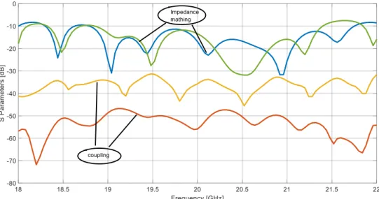
Simulation results of the array are shown in Fig. 2.8 and Fig. 2.9. As it can be observed, for the Tx and Rx configurations of the array antenna results present a good matching both E and H plane. It is also possible to notice good isolation between both different polarizations and different bands, as it was requested.
Vertical polarization Rx band
Horizontal polarization Rx band
Vertical polarization Rx band
Horizontal polarization Rx band
Vertical transition Rx band
Fig. 2.8 - Simulated S-parameters in Rx band of the array configuration
Fig. 2.9 - Simulated S-parameters in Tx band of the array configuration
The co-polar and cross-polar radiation pattern along E-plane and H-plane were simulated both for Rx and Tx elements as shown in Fig. 2.10 and Fig. 2.11, respectively. In both case, co-polar radiation patterns present a good behaviour with a broad beam well defined and without the presence of grating lobes as we
expected. A gain of 17dBi for Rx configuration and 18dBi was obtained for Tx configuration, respectively. In both operational bands the cross polarization level are well below 30dBi.
Fig. 2.10 - Radiation pattern at 20GHz
Fig. 2.11 - Radiation pattern at 30GHz
The good polarization purity of the radiating elements at both bands and the good isolation between different polarizations, make this antenna suitable also to
radiate or receive circularly polarized signals. In Fig. 2.12 and Fig. 2.13 are reported the radiation diagram of the RHCP and LHCP polarization.
Fig. 2.12 - RHCP radiation pattern at frequency of 20GHz
Fig. 2.13 - RHCP radiation pattern at frequency of 30GHz
2.2.3. Measurements
At this stage only a prototype of the single radiating element has been realized. The antenna has been fed with Huber-Suhner MMX connectors which is soldered at lowest layer of the stack up. A MMPX connector – K connector transition was
used to connect the antenna to the Network Analyzer. The antenna is shown in Fig. 2.14, Fig. 2.15 and Fig. 2.16.
Fig. 2.14 - Bottom view of the antenna
Fig. 2.15 - Top view of the antenna
Fig. 2.16 - Antenna with MMPX to K transition
Only the performance of S-parameters and gain of the single radiator have been measured.
The antenna was not measured in an anechoic chamber but it was realized a measurement setup on a bench. The antenna and a wideband horn were
positioned one in front of the other at a distance of 64cm which, considering that the longest side of the horn is 8cm, is in the horn far field The characteristics of the wide band horn are reported in the Tab. 2.2 .
Tab. 2.2 - Gain of the wide band horn
The overall system was shielded with absorbers. In Fig. 2.17 and Fig. 2.18 are shown the gain of the two polarizations of radiator. As it can be seen, measured gain present a frequency shift with respect to the simulated results. This behaviour is also clear in the trend of the S-parameters showed in Fig. 2.19 and Fig. 2.20. The values of the gain reported in Fig. 2.17 and Fig. 2.18 do not take into account the losses due to the connectors (0.35db) and transition (0.4dB) necessary to connect the antenna to the network analyser.
Frequency [GHz] Gain [dBi] Frequency [GHz] Gain [dBi]
15 15.3 28 19.5 17 16.8 30 19.7 18 17.5 32 19.1 19 17.8 34 19.3 20 18.2 35 19.2 21 18.8 36 19.1 22 18.9 38 18
Fig. 2.17 - Gain of the horizontal polarization in Rx band
Fig. 2.18 - Gain of the vertical polarization in Rx band
Fig. 2.20 - Horizontal polarization in Rx band
In Fig. 2.21 and Fig. 2.22 are shown the measured parameters in the Tx band. Even in this case, it is possible to observe a frequency shift.
Fig. 2.22 - S parameters of the horizontal polarization in Tx band
The frequency shift observed both in the measurements in Rx band and in Tx band are related to the manufacturing process. For the same reasons the vertical polarization TX resulted compromised and results are not shown here.
3.
Cylindrical Reflector Antenna for wireless
communication systems
3.1.
State of the Art
During the last years, the need of new mobile services and communication systems led to an overcrowded frequency spectrum. The allocation of the mm-Wave frequency is seen as a solution to this problem in both satellite and terrestrial communications. As far as satellite communications are concerned, the shift towards higher frequencies is shown by the number of high power Ka band satellites that has spawn the development of high performance user terminals with typology and size that change considerably according to the applications. As an example, a new breed of Satcom-On-The-Move (SOTM) terminals have been presented by several companies to offer internet services on vehicles, ships and airplanes. These terminals have to use high efficiency antennas of reduced size and weight to be mounted on mechanical pointing systems, as it was already discussed in the previous chapter. Earth fixed terminals do not pose the same constraints in weight and size as SOTM antennas. However, there are applications, like defence and security, where reduced size, light weight, man transportable terminals, quick to be deploys are needed. These antennas are usually very cumbersome to design as they have to provide good efficiency and compliance with challenging EIRP density masks on the satellite Geostationary
Orbit (GSO) plane, while maintaining a radiating surface as small as possible. For this reason arrays of waveguide radiators or reflector antennas are used. Similar challenges are faced when designing antennas for point to point (fixed beam) mm-Wave wireless links to be used in backhaul system for the current or the next generation of mobile communications (5G). As an example, the architecture of 5G will be composed by heterogeneous wireless network macro-cells overlaid by mmW small-macro-cells deployed in dense user areas (Fig. 3.1). In this scheme, mmW small-cell Access-Point (APs) will support massive data exchanges for mobile users with very high data rates, low latency, low interferences and low power consumption per bit. These AP will be connected between themselves and to the cellular network through high-capacity backhaul/fronthaul links which may be implemented over optical fibre or mmW poit-to-point wireless links.
Fig. 3.1 - 5G hybrid radio access architecture with a macro-cell providing microwaves access, mmW small cells and mmW backhaul.
The utilization of mmW terminals in backhaul links give the possibility to obtain high data rates without extreme increase in spectral efficiency in contrast to
centimetre wave cellular systems with highly complex techniques aimed at predominately achieving a higher spectral efficiency due to much smaller available bandwidths. These wireless links are capable of replacing fiber optics, because they are less costly and easier to deploy [7]. As in the case of satellite communications, they are required to be mechanically small, of high gain and suitable for integration with the radio. Microstrip circuits are appropriate for integration with active MMIC components, but they suffer from higher losses with increasing frequency as well as from the presence of cavity resonances when packaged. For these reasons, similarly to satellite communications, arrays of waveguides and reflector are the most common solutions.
Arrays and reflectors are both good solutions but none of them can be considered as optimal. Gain and overall efficiency of an array antenna depends mainly on the losses of the feed network. An array of metallic waveguide radiators may reach an aperture efficiency up to 80% when using a parallel fully branched (i.e. corporate) feed network. However, arrays of waveguides requires the design of complex feeding network which may become very challenging if multiband operation and beam tapering are required.
The efficiency of reflector antennas may be high due to their low losses, but reflectors suffer of spill over loss and non-uniform illumination, and they are not low profile. However, reflectors are simpler than array to build and they may be made lighter when carbon fiber or resins are used to build the reflecting surface. One well known issue of both structures is the fulfilment of regulations on radiated power density masks. To make radiation patterns complaining with regulations is not an easy task and usually the solution adopted is to use larger aperture to have narrower beams. Array with highly tapering BFN may be designed with a loss of efficiency and considerably increased complexity. However, arrays allows
for a simpler and effective solution exploiting the natural tapering observed considering the radiation pattern along the diagonal of a rectangular aperture. The reflector antennas are normally easier and cheaper to build and limit the complexity to the design of the feed. The most commonly used reflectors are axially-symmetric dual reflector antennas, typically Cassegrian and Gregorian systems [8], or their “displaced axis” or “ring focus” variants [9], [10], [11]. In these cases, a low profile may be obtained considering “deep dish” with reduced f/D ratio (<0.3). These antennas normally adopt self supported re-irradiating feed, like hat feed and splash plate feed, which do not use supports to improve blockage loss. However, the design of a feed able to ensure a good efficiency and fulfilling mask requirements at the same time is cumbersome, in particular when dual band operation have to be obtained.
In this chapter, a novel antenna which reduce the complexity and the cost related to the manufacture of an array is proposed. The terminal is based on a cylindrical reflector antenna .This solution retain the simplicity of the reflectors and alleviates the design of the feed. In fact, as it is in the case of arrays, the rectangular aperture of the cylindrical reflector can be used to exploit the radiation tapering on the diagonal plane. As an example, in the case of the satellite communications, power density masks are fulfilled by simply orienting the diagonal of the antenna on the satellite, without lengthy feed optimisation.
3.2.
Cylindrical Reflector antenna
A picture of the cylindrical reflector is shown in Fig. 3.2. The reflector is fed with a parallel plate in which a TEM mode is excited. The parallel plate radiate toward a corrugated hat feed which direct the field on the cylindrical reflector.
The antenna is linearly polarized, circular polarization may be achieved with the help of a printed polarizer placed on top of the reflector. The structure is
15cm 3 .7 5 c m 15cm
essentially composed by three parts: the parallel plate, the hat feed and the reflector. In the following the design of the three blocks will be described.
3.2.1. Parallel Plate
The hat feed is illuminated by a parallel plate waveguide fed with a rectangular horn. Due to the strong linear polarization of the feed, the radiation pattern on the antenna can be considered and optimized independently on the two principal planes. To obtain a flat field distribution to illuminate the hat feed, a parallel plate waveguide structure is used to feed the antenna.
Fig. 3.3 - Parallel plate structure
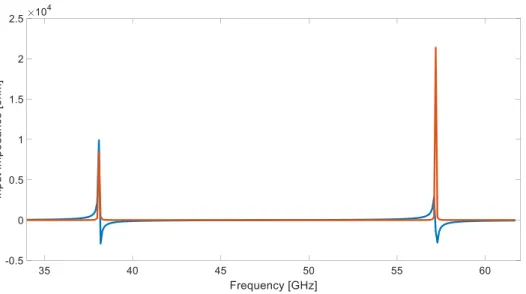
As shown in Fig.3.3, the parallel plate waveguide is composed by two different levels. In the first one, a horn antenna illuminates the parabolic reflector place in the ppw. The wave reflected by the parabolic reflector propagates to the second level through a coupling slot located between the two layers. In this way, it is possible to have a distribution field without the blockage effect. The PPW and the feeding horn have been optimized to have a flat field distribution and good taper
to reduce side lobes. In Fig.3.4, it is shown the field pattern inside the parallel plate top layer at the frequencies of 40GHz and 60GHz. As it is possible to see, the field distribution is quite flat along the aperture.
Fig. 3.4 Field distribution inside the PPW
In Fig. 3.5 is shown the radiated field corresponding to the field distribution reported in Fig. 3.4.
3.2.2. Hat Feed
3.2.2.1. General considerations
Hat feeds (Fig. 3.6) are self-supported, rear irradiating feed that have many advantages such as low side lobes level, low spillover losses and no blockage or scattering from support struts. A classic version of the hat feed is composed by a waveguide (the neck), a dielectric spacing (the head) and a corrugated structure (the hat). The corrugation of the hat brim is traditionally λ/4 deep causing the normal component of the E-field to be zero along the brim. To understand the behaviour of the Hat feed, let consider the definition of electromagnetic soft and hard surface.
Fig. 3.6 - Profile of the Hat Feed with its three main parts
Considering the boundary conditions of the E-field it is possible to define soft and hard surface for electromagnetic propagation. The electromagnetic soft and hard surfaces have polarizations independent boundary conditions (at the centre frequency) in contrast to a metallic conductor that has different boundary conditions for the tangential and normal components of the E-field. The soft and hard surfaces are realised by providing a metal conductor by an anisotropic surface impedance. This can be obtained by providing it with corrugations, or with
a strip-loaded dielectric layer. Generally, the hard surface will support waves with a maximum value of the E-field at the surface for any polarization, whereas the soft surface makes the amplitude of the E-field zero at the surface (Fig. 3.7).
Fig. 3.7 - Hard and soft surface structure
To understand how a soft surface works, let us now consider electromagnetic waves, and write the E-field as
𝐸⃗ = 𝐸𝑡𝑡̂ + 𝐸𝑙𝑙̂ + 𝐸𝑛𝑛̂
Where 𝑛̂ is the unit normal to the surface, and 𝑡̂ and 𝑙̂ are unit vectors tangential to it with 𝑡̂ normal to the direction of propagation of the wave and 𝑙̂ normal to 𝑡̂ and directed along the projection of the direction of propagation along surface. Thereby 𝑡̂ and 𝑛̂ specify transverse directions, and 𝑙̂ specifies the longitudinal direction (Fig. 3.8).
Fig. 3.8 - Ray-fixed coordinate system
We let 𝑙̂, 𝑡̂ and 𝑛̂ form a righthand orthogonal coordinate system. The boundary condition of a perfect conductor is the tangential components of the total E-field at any regular point of the scattering surface be zero:
𝐸𝑡 = 𝐸𝑙 = 0
If the conductor is located in a homogeneous dielectric (i.e. with constant permittivity) it is possible to use the previous conditions and Maxwell’s equations 𝑉⃗ · 𝐸⃗ = 0 to show that ∂𝐸𝑛/ ∂n=0, or generally
∂𝐸𝑛 ∂n +
(𝑟1+ 𝑟2) 𝑟1𝑟2
𝐸𝑛 = 0
If the surface is curved with r1 and r2 the two principal radii of curvature. Therefore, if we consider each of the three field components separately, we may state that a perfect conductor corresponds to a soft boundary for the tangential field components 𝐸𝑡 𝑎𝑛𝑑 𝐸𝑙, and to a nearly hard boundary for the normal field component 𝐸𝑛. To realize a soft surface, let consider a surface with transverse
𝑣 ≪ 𝑤 + 𝑣 ≪ 𝜆/2
Fig. 3.9 - Transverse corrugations
Where w is the width of the corrugations, v is the width of the edges between them and λ is the wavelength. The corrugations are narrow, so that a number of discrete modes can describe the field solution within them. When the condition 𝑣 ≪ 𝑤 + 𝑣 ≪ 𝜆/2 is satisfied there will be only one nonevanescent mode present within the corrugations. This is a TEn Mode with an 𝐸𝑙 component only, and this
component will have no longitudinal variation within each corrugation. Notice that a TEM mode could be present in the grooves but the TEM mode is a degeneration of a TM mode rather than a TE one. The 𝐸𝑙-field inside the corrugations is generally accompanied by 𝐻𝑡 𝑎𝑛𝑑 𝐻𝑛 fields, but we can choose the corrugation depth d that transform 𝐻𝑡 to
𝐻𝑡 = 0 𝑜𝑟 𝑒𝑞𝑢𝑖𝑣𝑎𝑙𝑒𝑛𝑡𝑙𝑦 |𝑍𝑙| = ∞
At the outer surface 𝑆0. At the edges between the corrugations 𝐻𝑡 = 0 as well
because there can be no longitudinal currents when v→ 0. The 𝐸𝑡 and 𝐻𝑙 components at 𝑆0 are determined by the edges between the corrugations. They short circuit 𝐸𝑡 very efficiently with strong transverse currents, so that
𝐸𝑡 = 0 𝑜𝑟 𝑒𝑞𝑢𝑖𝑣𝑎𝑙𝑒𝑛𝑡𝑙𝑦 𝑍𝑡 = 0
Therefore from these two condition related to 𝐸𝑡 and 𝐻𝑡 the transversely
corrugated surface is a soft surface, if d is chosen so that 𝐻𝑡 = 0 is satisfied ad 𝑆0. The value of d is related to the choice of the surface and corrugations. The simplest case is a plane surface with a plane wave incident on it. We let the corrugations be straight and transverse to the direction of incidence of the wave. Then, the 𝐸𝑙 field of the 𝑇𝐸𝑛 mode within them is given by
𝐸𝑙 = sin (𝑘𝑛 + 𝑘𝑑)
Where k=2π/λ is the wavenumber and n is the dimension variable along 𝑛̂, with n=-d at the inner surface 𝑆𝑖 and n=0 at 𝑆0. 𝐸𝑙 satisfies the boundary condition 𝐸𝑙 =
0 at n=-d. The condition 𝐻𝑡 = 0 applied to the 𝑇𝐸𝑛 mode is by using Maxwell’s
equation 𝑉⃗ · 𝐸⃗ = −𝑗𝜇ѡ𝐻⃗⃗ equivalent to
𝜕𝐸𝑙
𝜕𝑛 = 0 𝑎𝑡 𝑆0 That is satisfied and thus the surface is soft when
𝑑 = 𝜆/4
3.2.2.2. The hat feed for a cylindrical reflector – Theory
The hat feed used in the antenna shown in Fig. 3.2 is illuminated by a PPW which mainly radiates a TEM mode. In this condition, the hat feed behaves like a soft surface and its working principle relies on its capability to sustain and to guide
surface waves along corrugations and to direct them towards the reflectors, rather than to simply reflect them as it is done in the case of splash plate feed. In fact, in the hat feed waves radiated by the PPW guide are reflected by the cuspid towards the corrugated surface, on which TM surface waves are excited. To better define guidelines to the design of the hat feed, it is useful to ascertain the characteristics of the TM surface waves propagation on a corrugated plane. The analysis presented in the following, it is not rigorous, however numerical software currently available allows the access to meaningful numerical data in short time. What it is presented here will prove useful to have a broader comprehension of the phenomena and to define starting points for the optimization process. In Fig. 3.10 is shown an infinite corrugated conducting plane. The structure extends to infinity in both z and y direction.
As it can be seen, the structure is periodic, with period 𝐿 = 𝑊 + 𝑡and it extends infinitely along the z axis. Also, it is of an infinite extent along the y axis as well, so we will assume that the fields do not depend on the y coordinate. As the structure is periodic a Floquet expansion of the fields is considered in the region external to the grooves (region II in Fig.3.10). A TEM solution is investigated
x
d
W
t
z
II
I
within the grooves (region I) and a TM surface waves is considered in region II. Under these positions the Helmholtz equation for the 𝐻𝑦 field is considered
∇2𝐻𝑦(𝑥, 𝑧) + 𝑘02𝐻
𝑦(𝑥, 𝑧) = 0 (1)
Separation of variables leads to the following two equations for 𝐻𝑦(𝑥, 𝑧) = 𝑔(𝑥)𝑓(𝑧) 𝜕2𝑔(𝑥) 𝜕𝑥2 + 𝑘𝑥 2𝑔(𝑥) = 0 𝜕2𝑓(𝑧) 𝜕𝑧2 + 𝑘𝑧 2𝑓(𝑧) = 0 (2) with 𝑘02 = 𝑘𝑥2+ 𝑘𝑧2.
The periodicity of the structure along z induces a degree of periodicity on the solutions as well both region (I) and (II). In region (II) one can pose that 𝑓(𝑧) is almost periodic with period 𝐿 but a phase shift accumulated at each cell:
𝑓(𝑧 + 𝐿) = 𝑓(𝑧)𝑒−𝑗𝜓 (3)
𝑓(𝑧) it would be conveniently expressed as a Fourier series. To do this one first consider the function
𝐹(𝑧) = 𝑓(𝑧)𝑒𝑗(
𝜓
𝐿)𝑧 (4)
𝐹(𝑧) is a periodic function as: 𝐹(𝑧 + 𝐿) = 𝑓(𝑧 + 𝐿)𝑒𝑗( 𝜓 𝐿)(𝑧+𝐿) = 𝑓(𝑧 + 𝐿)𝑒𝑗𝜓𝐿𝑧 𝑒𝑗𝜓= 𝑓(𝑧)𝑒−𝑗𝜓𝑒𝑗𝜓𝑧 𝑒𝑗𝜓 = (5)
= 𝑓(𝑧)𝑒𝑗(
𝜓
𝐿)𝑥 = 𝐹(𝑧)
So 𝐹(𝑧) is now expressed as Fourier series
𝐹(𝑧) = ∑ 𝐴𝑛𝑒𝑗2𝑛𝜋𝐿 𝑧 𝑛=+∞
𝑛=−∞
(6)
Substituting expression (3) one has
𝑓(𝑧) = ∑ 𝐴𝑛𝑒𝑗( 2𝑛𝜋 𝐿 𝑧− 𝜓 𝐿𝑧) 𝑛=+∞ 𝑛=−∞ (7)
Expression (7) is the Floquet expansion of 𝑓(𝑧). In the following we will make use of the more meaningful notation
𝑓(𝑧) = ∑ 𝐴𝑛𝑒−𝑗( 2𝑛𝜋 𝐿 +𝛽)𝑧 𝑛=+∞ 𝑛=−∞ (8)
Going back to equations (1), under the assumption that the width of the grooves 𝑊 ≪ 𝜆 to allow the propagation of 𝑇𝐸𝑀 mode only, one can write the following solutions Region (I) 𝐻𝑦𝐼(𝑥, 𝑧) = 𝐴𝑒−𝑗𝑘𝑥𝐼𝑥+ 𝐵𝑒𝑗𝑘𝑥𝐼𝑥 𝐻𝑦𝐼(𝑥, 𝑧 + 𝑁𝐿) = 𝐻 𝑦(𝑥, 𝑧)𝑒−𝑗𝛽𝑁𝐿 𝐸𝑧𝐼(𝑥, 𝑧) = − 𝑘𝑥 𝐼 𝜔𝜀0(𝐴𝑒 −𝑗𝑘𝑥𝐼𝑥− 𝐵𝑒𝑗𝑘𝑥𝐼𝑥) (9)
𝐸𝑧𝐼(𝑥, 𝑧 + 𝑁𝐿) = 𝐸 𝑧𝐼(𝑥, 𝑧)𝑒−𝑗𝛽𝑁𝐿 Region (II) 𝐻𝑦𝐼𝐼 = ∑ 𝐴𝑛𝑒−𝑗(2𝑛𝜋𝐿 +𝛽)𝑧𝑒−𝑗𝑘𝑥𝑛𝐼𝐼𝑥 𝑛=+∞ 𝑛=−∞ 𝐸𝑥(𝑥, 𝑧) = 1 𝜔𝜀0 ∑ 𝐴𝑛( 2𝑛𝜋 𝐿 + 𝛽) 𝑒 −𝑗(2𝑛𝜋𝐿 +𝛽)𝑧 𝑒−𝑗𝑘𝑥𝑛𝐼𝐼𝑥 𝑛=+∞ 𝑛=−∞ 𝐸𝑧(𝑥, 𝑧) = − 1 𝜔𝜀0 ∑ 𝐴𝑛𝑘𝑥𝑛 𝐼𝐼 𝑒−𝑗(2𝑛𝜋𝐿 +𝛽)𝑧 𝑒−𝑗𝑘𝑥𝑛𝐼𝐼𝑥 𝑛=+∞ 𝑛=−∞ (10)
Under the assumption that 𝑊 < 𝜆/2 only a 𝑇𝐸𝑀 mode is present in the groove and in the set of equations (9) 𝑘𝑥𝐼 = 𝑘
0. In (9) the second equation states that the
electromagnetic field into the grooves do not change but a phase contribution which is accumulated at each cell. This is essential to satisfy the matching of tangential components between internal and external tangential fields at the grooves aperture. In (10) one has
𝑘02 = 𝑘𝑥𝑛𝐼𝐼 2+ (2𝑛𝜋 𝐿 + 𝛽)
2
(11)
Considering a surface waves which attenuates along 𝑥 direction one can pose 𝑘𝑥𝑛𝐼𝐼 = −𝑗𝛼
𝑥𝑛𝐼𝐼 . Equation (11) then becomes
𝑘02 = −𝛼𝑥𝑛𝐼𝐼 2+ (
2𝑛𝜋 𝐿 + 𝛽)
2
(12)
The expansion presented in equations (9) and (10) have to be matched at the interface between region (I) and region (II).
𝐻𝑦𝐼(𝑑, 𝑧) = 𝐻 𝑦𝐼𝐼(𝑑, 𝑧) 𝑁𝐿 + 𝑡 < 𝑧 < 𝑁𝐿 + 𝑊 𝐸𝑥𝐼𝐼(𝑑, 𝑧) = 0 𝑁𝐿 < 𝑧 < 𝑁𝐿 + 𝑡 𝐸𝑥𝐼(𝑑, 𝑧) = 𝐸 𝑥𝐼𝐼(𝑑, 𝑧) 𝑁𝐿 + 𝑡 < 𝑧 < 𝑁𝐿 + 𝑊 𝐸𝑥𝐼(0, 𝑧) = 0 𝑁𝐿 + 𝑡 < 𝑧 < 𝑁𝐿 + 𝑊 (13)
The last of equation in (13) states that the tangential components of the electric field is zero at 𝑥 = 0. When this condition is used the expressions for 𝐻𝑦 and 𝐸𝑧 in (9) become 𝐻𝑦𝐼(𝑥, 𝑧) = 2𝐴𝑐𝑜𝑠(𝑘0𝑥) 𝐸𝑧𝐼(𝑥, 𝑧) = 2𝑗𝐴 𝑘𝑥𝐼 𝜔𝜀0 sin (𝑘0𝑥) (14)
The continuity of the electric and magnetic tangential components for 𝑥 = 𝑑 results into the following equations
𝐴𝑐𝑜𝑠(𝑘0𝑑) = ∑ 𝐴𝑛𝑒−𝑗( 2𝑛𝜋 𝐿 +𝛽)𝑧𝑒−𝑗𝑘𝑥𝑛𝐼𝐼 𝑑 𝑛=+∞ 𝑛=−∞ 𝑁𝐿 + (𝐿 − 𝑊) < 𝑁𝐿 + 𝑊 𝑗𝐴 𝑘0 𝜔𝜀0 sin(𝑘0𝑑) = − 1 𝜔𝜀0 ∑ 𝐴𝑛𝑘𝑥𝑛 𝐼𝐼 𝑒−𝑗(2𝑛𝜋𝐿 +𝛽)𝑧 𝑒−𝑗𝑘𝑥𝑛𝐼𝐼𝑑 𝑛=+∞ 𝑛=−∞ 𝑁𝐿 + (𝐿 − 𝑊) < 𝑁𝐿 + 𝐿 (15)
0 = − 1 𝜔𝜀0 ∑ 𝐴𝑛𝑘𝑥𝑛𝐼𝐼 𝑒−𝑗( 2𝑛𝜋 𝐿 +𝛽)𝑧𝑒−𝑗𝑘𝑥𝑛𝐼𝐼𝑑 𝑛=+∞ 𝑛=−∞ 𝑁𝐿 < 𝑧 < 𝑁𝐿 + (𝐿 − 𝑊)
where the factor 2 is now included in the coefficient 𝐴. It is easy to demonstrate that functions 𝑒−𝑗(2𝑛𝜋𝐿 +𝛽)𝑧 are orthogonal on the interval [0, 𝐿] having
∫ 𝑒𝑗(2𝑚𝜋𝐿 +𝛽)𝑧 𝐿
0
𝑒−𝑗(2𝑛𝜋𝐿 +𝛽)𝑧𝑑𝑧 = 𝛿𝑛𝑚𝐿
Testing equations (15) with 𝑒𝑗( 2𝑚𝜋
𝐿 +𝛽)𝑧 and integrating along 𝑧 between −𝐿/2 and 𝐿/2 (for convenience the origin of the axis is now considered at the center of the groove) one has
𝐴𝑐𝑜𝑠(𝑘0𝑑) 𝑠𝑖𝑛𝑐(𝛽𝑚𝑑) = 𝐴𝑚𝑒−𝑗𝑘𝑥𝑚𝐼𝐼 𝑑
𝑗𝐴𝑘0sin(𝑘0𝑑) 𝑠𝑖𝑛𝑐(𝛽𝑚)𝑑 = −𝐴𝑚𝑘𝑥𝑚𝐼𝐼 𝑒−𝑗𝑘𝑥𝑚
𝐼𝐼 𝑑
(16)
where 𝛽𝑚= 2𝑚𝜋/𝐿 + 𝛽.
Considering now that for a surface wave in region (II) one has 𝑘𝑥𝑚𝐼𝐼 = −𝑗𝛼
𝑥𝑚𝐼𝐼 with
𝛼𝑥𝑚𝐼𝐼 > 0, by dividing the second equation in (16) by the first one, one obtains the
following dispersion relation
𝑘0tan(𝑘0𝑑) = 𝛼𝑥𝑚𝐼𝐼 (17)
Equation (17) is not useful to exactly determine the propagation constant 𝛽, but it shows that a surface wave may propagate in region (II) only if tan(𝑘0𝑑) > 0, which means that 𝑇𝑀 surface waves on a corrugated conducting plane have a bandpass/stopband characteristic. In particular, one has surface wave propagation if 𝑛𝜆/2 < 𝑑 < (2𝑛 + 1)𝜆/4, in particular for 𝑑 < 𝜆/4.
The corrugated plane permits also the propagation of waves which are not bound to the conducting surface but that may radiate. Those waves, named leaky waves or fast waves, to distinguish them from the surface waves which propagates with a speed lower than the speed of light, may be excited under certain conditions. In this case the propagation constant along 𝑧 direction 𝛽𝑛has no more the form
taken in the case of surface waves but it can be written as 𝛽𝑛− 𝑗𝛼 , which states that as the wave propagates along the corrugations it loses power in form of radiated fields. In this case the propagation constant along 𝑥 can be expressed as
𝑘𝑥𝑛𝐼𝐼 2 = 𝑘02 − 𝛽𝑛2+ 2𝑗𝛼𝛽𝑛 (18)
Considering the relation (18) for 𝛼 = 0 and 𝑛 = 0 the (𝑘0𝐿, 𝛽0𝐿) plane can be
considered.
Fig. 3.11 - Radiation and surface wave regions in the k0 L-β0 L plane
The regions in Fig. 3.11 correspond to the conditions: Fast waves (Radiation) 𝑘0 > 𝛽0 𝑜𝑟 𝑘0/𝛽0 > 1 Slow waves (Surface waves ) 𝑘0 < 𝛽0 𝑜𝑟 𝑘0/𝛽0 < 1
Fig. 3.12 - Radiation and surface wave regions in the k0L-βnL diagram
Considering Floquet harmonics other than 𝑛 = 0, the diagram is periodic as shown in Fig.3.12, where the index of the harmonics up to 𝑛 = ±3 is shown. The gray regions correspond to surface waves regions. As it can be seen surface waves do not exist for 𝑘0𝐿 > 𝜋, i.e., 𝐿 > 𝜆/2.
The considerations shown up to know defined a starting point for the design and the optimisation of the hat feed. In particular one needs grooves with 𝑑 < 𝜆/4 and 𝑊 < 𝜆/2.
3.2.2.3. Single and Dual and hat feed for a cylindrical reflector In this section is presented the design of a dual band hat feed for a cylindrical reflector. It is anticipated that a double corrugations is adopted in order to obtain a good performance in terms of both impedance matching and radiation pattern in the bands of interest.
4 .375 mm 0.5mm 2 .5 mm
Fig. 3.13 - Dual band Hat feed
As a starting point a first attempt to illuminate the reflector by a hat feed with a single corrugation was done. The had feed has been designed considering only the radiation on the plane of interest (E-plane). The structure of the hat feed is shown in Fig. 3.14. Corrugation depth was firstly set to λ/4 and then quickly optimized. An attempt to find a corrugation length that could be used in both bands of interest was done. The feed has been optimized adjusting length and width of the cusp and length and width of corrugation. To ease a future fabrication process corrugations have been taken of equal length and width instead of using corrugations with different length and width.
Fig. 3.15 - Reflection coefficient in Rx-band
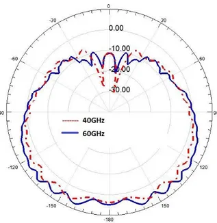
Fig. 3.17 - Simulated radiation pattern of the Hat Feed at the 40GHz and 60GHz
The optimized hat feed has a depth (L) of 1mm and width (w) 3mm. Fig. 3.15 and Fig. 3.16 show the simulated S11 parameters on the two bands of interest. S11
has been considered at the input of the parallel plate that illuminates the feed. Furthermore, in Fig. 3.17 are shown the radiation patterns of the hat feed at 40GHz and 60GHz. As it can be observed, the feed has a good radiation pattern at the lower frequency, with a 8dB roll off, but at the highest frequency the pattern deviates considerably from the other one. This would results in a degraded pattern of the overall antenna with a high level of side lobes. In order to obtain a dual band hat feed two possible solutions could be applied: the using of a dielectric inside the corrugations or the using of a double corrugations. Following the second choice, the previous structure has been modified adding a second corrugation as it is shown in Fig. 3.13. While the depth of both corrugations affect the feed performances, one can say that the shortest corrugation controls the higher band while the longer one controls the lower band. The starting point of the optimization was set the resonance points exactly at the two-mid bands. In
(Fig. 3.18) is shown the input impedance of Fig. 3.14) , length L and width W were chosen to make the structure resonate as shown in Fig. 3.18.
Fig. 3.18 - Input impedance of the single corrugation
A lengthy optimisation process gave the following geometry:
𝑑1 = 4.375𝑚𝑚, 𝑑2 = 1.75𝑚𝑚, 𝑤1 = 0.5𝑚𝑚, 𝑤2 = 0.375𝑚𝑚
Where 𝑑1 and 𝑑2 are respectively the depth of the longer corrugation and of the shorter one while 𝑤1 and 𝑤2 are the width (Fig. 3.19).
Fig. 3.19 - Hat Feed with a dual corrugations
D1
D2
W1
Length and width of the grooves were optimised trying to have a good level of side lobes and good efficiency over the two bands. Considering the input impedance of the corrugation, as it was done for the starting structure, it is possible to verify that in order to have a propagation of the TM mode, the resonance point is shifted toward to frequencies lower than the starting values (Fig. 3.20).
Fig. 3.20 - Input impedance of the dual corrugation at the optimal point
The ratio between the depth of the lower corrugation and the higher one gives the possibility to obtain good performance in both frequency range without degradation on the pattern of the antenna. In order to optimize the illumination of the reflector, a tapering of 8 dB has been realized on the radiation pattern of the hat feed (Fig. 3.21). This behaviour makes possible the reduction of the spillover losses of the overall antenna.
Fig. 3.21 - Simulated radiation pattern of the hat feed with two corrugations at the centre frequency of the two bands
A further optimization, in order to minimize the effects of multiple reflections between reflector and feed a Gaussian vertex plate was introduced.
3.2.2.4. Gaussian Vertex plate
Multiple reflections between reflector and feed may have a critical effect on the reflection coefficient and the radiation pattern. By introducing a flat vertex plate at the centre of the reflector, the multiple reflections can be reduced and the reflection coefficient improved. Positive effects have also been seen in terms of reduction of side-lobes levels and increased directivity due to reduced centre blockage and multiple reflections between reflector and feed as investigated in [12]. The contribution of the multiple reflections and its influence on G/T was analysed further in [13] using the method of moment. The evolution of the vertex plates eventually lead to a Gaussian shape for improved performance [14]. The Gaussian vertex plate can make the reflected field from the reflector a null at the focus of the reflector where its feed is located, and this therefore minimizes the degrading effect of the multiple reflections and reduces the diffractions from the
brim of the hat. In addition to this, the Gaussian vertex plate reduces the far-out sidelobes. The derivations lead to the following design formulas for the shape of the Gaussian vertex plate (Fig. 3.22):
𝑡 = 𝑡0𝑒−( 𝜌 𝜌0) 2 , With 𝑡0 = 0.15𝜆 𝜌0 = 0.5√(𝐹𝜆)
Fig. 3.22 - Gaussian vertex plate in a reflector antenna
3.2.3. Cylindrical reflector realization and measurements
Once that all the components of the antenna has been optimized, the dual band cylindrical reflector was simulated, manufactured and measured. The overall structure is proposed in Fig. 3.23- Fig. 3.24