Procedia Engineering 168 ( 2016 ) 1140 – 1143
1877-7058 © 2016 The Authors. Published by Elsevier Ltd. This is an open access article under the CC BY-NC-ND license (http://creativecommons.org/licenses/by-nc-nd/4.0/).
Peer-review under responsibility of the organizing committee of the 30th Eurosensors Conference
doi: 10.1016/j.proeng.2016.11.376
ScienceDirect
Available online at www.sciencedirect.com
30th Eurosensors Conference, EUROSENSORS 2016
NiO/ZnO nanowire-heterostructures by vapor phase growth for gas
sensing
Navpreet Kaur
a*, Elisabetta Comini
a, Nicola Poli
a, Dario Zappa
a, Giorgio Sberveglieri
a aSENSOR Laboratory, University of Brescia and CNR-INO, Via D. Valotti 9, 25133 Brescia, ItalyAbstract
Physical interface between p and n-types semiconducting materials known as p-n junction or heterojunction represents the key technology in many electronic and optoelectronic devices such as gas sensors. In this work we are presenting a novel method for the growth of NiO/ZnO (NWs) based heterostructures with vapor phase mechanism and their preliminary sensing study for acetone. To fabricate the NiO/ZnO NWs heterostructures, firstly NiO nanowires were grown on alumina substrates with Vapor-Liquid-Solid (VLS) method and then Vapor-Solid (VS) method was used for the growth of ZnO nanowires on as grown NiO nanowires. The surface morphology of NiO nanowires and NiO/ZnO heterostructures were investigated with scanning electron microscopy (FE-SEM). Raman spectroscopy has also been used for the structural characterization of heterostructures. A set of conductromertric sensing devices based on NiO/ZnO heterostructures have been prepared. The preliminary sensing performance of NiO/ZnO NWs heterostructure devices towards acetone at temperature of 400ºC is reported in this work.
© 2016 The Authors. Published by Elsevier Ltd.
Peer-review under responsibility of the organizing committee of the 30th Eurosensors Conference.
Keywords: Nickel oxide; Zinc oxide; Sputtering; Nanowires; Heterostructure; Gas senosr.
1. Introduction
Solid-state metal oxide gas sensors based on one-dimensional nanostructures have been widely used in applications from health and safety. Among the metal oxides, ZnO (n-type) has a wide band gap (3.37eV), non-toxic, environmentally stable, and most abundant elements in earth's crust. On the other hand, NiO (p-type) has also
* Corresponding author. Tel.: Tel.: +39-030-371-5873; fax: +39-030-209-1271.
E-mail address: [email protected]
© 2016 The Authors. Published by Elsevier Ltd. This is an open access article under the CC BY-NC-ND license (http://creativecommons.org/licenses/by-nc-nd/4.0/).
1141
Navpreet Kaur et al. / Procedia Engineering 168 ( 2016 ) 1140 – 1143
wide band gap (3.6-4.0eV) used for the fabrication of electro-chromic devices. In literature these two semiconducting materials has been widely investigated [1]. Further, in nanomaterials based heterostructures, due to strong heterointeractions between the closely packed interfaces, their performances are considered as more superior and complex [2]. Herein, we present a first time report on growth of NiO/ZnO heterostructure nanowires growth with vapor phase mechanism.
2. Experiment
2.1. Substrates preparation
Alumina substrates (4mm2) were used to grow the NiO/ZnO heterostructures. The substrates were cleaned in ultrasonic cleaner with acetone for 15 min and dried with synthetic air. An ultrathin layer of gold (Au) catalyst was deposited on alumina substrates by using magnetron sputtering (Kenotec Sputtering system). Different deposition parameters such as 50W argon plasma, 5×10⁻³ mbar, 7SCCM Ar flow were used for deposition of gold catalyst. While for the deposition of ZnO on top of NiO nanowires no catalyst has been used.
2.2. VLS growth process for NiO nanowires
For the growth of NiO nanowires, an alumina tubular furnace (Custom design based on a Lenton furnace) was used. NiO powder was used as source material. The powder was heated at 1400°C to induce evaporation and pressure inside the alumina tube was kept at 1 mbar. The substrates were placed in comparable low temperature region at 930°C. Argon gas of 100SCCM was used to transport NiO vapours towards catalyst deposited alumina substrates. As the evaporated material reaches low temperature region, it starts to condensate on the substrates in the form of NiO nanowires [3].
2.3. VS growth process for ZnO nanowires
ZnO nanowires were grown onto the NiO nanowires deposited substrates using VS technique in tubular furnace. Growth process of ZnO nanowires was performed without using any metal catalyst inside the tubular furnace, at evaporation temperature of 1100ºC, 100SCCM argon flow.
2.4. Morphological and structural characterization
The surface morphology of deposited NiO nanowires and NiO/ZnO heterostructures was examined using SEM (Zeiss, Leo1525 Gemini model; Carl Zeiss AG, Oberkochen, Germany) operated at 3-5kV. Samples were fixed on metallic stub with a carbon-based glue to reduce sample charging during observation.
Raman spectra of NiO/ZnO heterostructure along with individual NiO and ZnO nanowires were measured using a HORIBA monochromator iHR320 configured at room temperature with a grating of 1800gmm−1, coupled to a Peltier-cooled Synapse CCD. A He-Cd laser (442nm) was focused on the sample by a fiber coupled optical microscope (HORIBA) at 100×magnification. Spectra were recorded in the wavelength of 200-1800cm−1 range.
2.5. Device Fabrication
For the fabrication of sensing devices, we firstly deposited a TiW adhesion layer by DC magnetron sputtering (70W argon plasma, @ 300°C, 5.5×10⁻³ mbar), then we deposited interdigited platinum contact using the same conditions explained before. A platinum heater was deposited on the back side of alumina substrate via same procedure used for contact deposition. Finally prepared device was mounted on TO packages using electro soldered gold wires.
The conductrometric response of these heterostructured sensing device was measured towards acetone at different concentrations. The total flow inside chamber was 200SCCM mixed with the synthetic air. Measurements
1142 Navpreet Kaur et al. / Procedia Engineering 168 ( 2016 ) 1140 – 1143
were obtained by keeping the climatic chamber at 20°C, with a relative humidity equal to 50% and applying 1V to the sensor devices.
3. Results
Figure 1(a) shows the SEM image of NiO nanowires, while figure 1(b) represents the SEM image of NiO/ZnO heterostructures. The ZnO nanowires seem to cover effectively the whole NiO nanowires. The diameter of NiO nanowires was found to lie in tenth order of nanometers.
Fig. 1. (a) SEM image of NiO nanowires. (b) SEM image of NiO/ZnO heterostructures nanowires.
Figure 2 reports the Raman spectra of NiO/ZnO heterostructure along with individual NiO and ZnO nanowires spectra. The peaks of NiO were clearly observed at 1490cm-1, 900cm-1 and 750cm-1. While the spectra peak obtained at 1100cm-1 has a bordering due the overlapping of NiO and ZnO peaks 1090cm-1 and 1140cm-1 respectively.
1143
Navpreet Kaur et al. / Procedia Engineering 168 ( 2016 ) 1140 – 1143
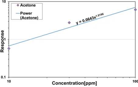
Fig. 3. Calibration curves for NiO/ZnO heterostructure sensor devices towards Acetone. At optimal working temperature 400°C, Relative humidity of 50% @ 20°C
The calibration curve has been drawn in Figure 3 at optimal working temperature of sensors. This curve was fitted by the typical power trend law for metal oxide sensors, and values of constants A and B was found to be 0.06 and 1.02 respectively. Considering a minimum response value of 1, the detection limit was found to be 14ppm for NiO/ZnO heterostructures nanowire sensors.
4. Conclusion
In conclusion, the NiO/ZnO based heterostructure nanowires were synthetized with vapor phase technique and were found to be densely packed. The sensitivity of the sensor was tested towards acetone and at different concentrations at their optimal working temperature of 400°C with relative humidity of 50%. The detection limit was found for heterostructured sensor was 14ppm. From these interesting results, the sensitivity of these sensors for other reducing and oxidizing gases is under investigation.
Acknowledgements
This work was supported by the European Community’s 7th Framework Programme, under the grant agreement n° 611887 “MSP: Multi Sensor Platform for Smart Building Management”.
References
[1] E. Comini, C. Baratto, G. Faglia, M. Ferroni, A. Panzoni, D. Zappa, G. Sberveglieri, Metal oxide nanowire chemical and biochemical sensors. J. Mater. Sci., 2013, pp. 2911-2931.
[2] R. Miller, A. Akbar, A. Morris, Nanoscale metal oxide-based heterojunctions for gas sensing: A review, Sens. Actuator B, 2014, pp. 250-272. [3] N. Kaur, E. Comini, D. Zappa, N. Poli, G. Sberveglieri, Nickel oxide nanowires: vapor liquid solid synthesis and integration into a gas