UNIVERSITÀ DEGLI STUDI DI CATANIA FACOLTÀ DI SCIENZE MM. FF. NN. DIPARTIMENTO DI SCIENZE CHIMICHE Dottorato Internazionale di Ricerca in Scienze Chimiche
XXIV Ciclo
Titanium Dioxide Nanoparticles
in the Field of Conservation of Cultural Heritage
Coordinatore: Prof. Corrado Tringali Tutor: Prof. Enrico Ciliberto
Dottorando: Dr. Pietro Gemmellaro
A.A. 2008-2011
Table of Contents
Acknowledgements ... I Keywords ... III List of Abbreviations ... IV
Conservation Problems and Nanotechnology Solutions ... 1
References ... 7
Nanotechnology ... 9
Introduction ... 9
Classification of nanomaterials ... 11
Properties of nanomaterials ... 12
Size-dependent properties of nanocrystals ... 17
Synthesis approaches and techniques ... 23
References ... 25
Catalysis ... 28
Introduction ... 28
Photocatalysis ... 29
General applications of photocatalysis ... 35
Nanoparticles catalysis ... 35
References ... 39
Titanium Dioxide ... 42
Introduction ... 42
TiO2 as nano-photocatalyst ... 47
Modification of TiO2 properties ... 53
References ... 55
Nanostructure Synthetic Methods ... 58
Introduction ... 58
Sol-gel method ... 59
Chemistry of sol-gel methods ... 62
Advantages of sol-gel methods... 64
References ... 66
Thin Film Deposition Methods ... 68
Introduction ... 68
Spin coating method ... 69
References ... 73
Experimental ... 76
Chemicals and materials ... 76
Synthesis of nanoparticles ... 76
Thermal analysis ... 80
SEM ... 82 DLS ... 83 XPS ... 84 UV-Vis spectrophotometry ... 84 Raman spectroscopy ... 85
Deposition of TiO2 nanoparticles on corning glasses ... 86
Optical properties of thin films ... 88
Results and Discussion ... 89
Thermal analysis ... 90
XRD ... 94
Raman spectroscopy ... 97
SEM ... 99
XPS ... 103
Optical properties of thin films ... 111
References ... 118
Photocatalytic Activities on Gases ... 120
Introduction ... 120
Theoretical background ... 120
Experimental ... 121
Results and discussions ... 128
References ... 134
Photocatalytic Activities on Aqueous Systems ... 135
Introduction ... 135
Theoretical background ... 136
Experimental ... 137
Results and discussions ... 141
References ... 150
I
Acknowledgements
I would like to express my sincere gratitude and appreciation to my research supervisor, Prof. Enrico Ciliberto, for guidance, support and patience towards the completion of this work, with a lot of passion, and also for our many scientific and not scientific discussions.
My sincere appreciations also extend to Prof. Geoffrey Allen, Interface Analysis Centre (University of Bristol, UK), and his Ph.D. student, James MacFarlane, who have provided assistance especially for gas photocatalytic experiments.
Grateful acknowledgements are to polish group of Prof. Danuta Kaczmarek (Politechnika Wrocławska, Wrocław): Dr. Jaroslaw Domaradzki, PhD students Michał Mazur, Damian Wojcieszak and Karolina Sieradzka for their collaboration, advice and valuable suggestions particularly in the method of conducting a research. I also wish to thank Mr. Eugeniusz Prociów, group technician who have provided assistance at instruments technology. I have to say thanks to this great foreign experience, without which I wouldn‟t know very special people, such as Marco Messina, Claudio Siracusano, Gabriele La Rosa, Luca Matarese and many others. This was probably one of the most beautiful periods of my life, and not only for pints (małe piwo) or discotheques for which I‟ll always have a special place in my thoughts and heart.
Special thanks to Dr. Ezio Viscuso for the help with SEM images and the EDX sample characterizations. Many thanks to all
the people who helped me to handle experiments and gave me access to their equipment as well as support and discussion of obtained results: Prof. Graziella Malandrino and Dr. Rita Catalano for XRD measurements, Prof. Salvatore Giuffrida for DLS techniques, Dr. Alessandro Motta for XPS equipments, and Prof. Raffaele Bonomo for UV-Vis spectrophotometry.
A sincere thanks also goes to the Erasmus student Magdalena Zalesakova, who helped me in reading and correcting this Ph.D. thesis as well as Dr. Cosimo Fortuna. I would like to thanks to Giuseppe Trusso for his great help for the graphic layout in this thesis.
Thanks to Ph.D. coordinator Prof. Corrado Tringali and Ph.D. officer Sabrina Tosto, for the very nice working atmosphere and great help in the bureaucracy, as well as all my Ph.D. colleagues.
Lastly, I would like to acknowledge my family and Cinzia Catanzaro for their love, understanding and support throughout my work.
And last but certainly not least finally I would like to extend endless thanks to my friends and family for helping me get through the past three years. I am also grateful to all people helping me during the PhD period and which are not mentioned by name.
An acknowledgement in my thesis is just a small gesture and doesn‟t truly represent how much I appreciate the influence that many people have had on my life.
III
Keywords
TiO2, doped, titania, titanium dioxide, metal oxide, nanostructure,
nanoparticles, sol-gel, spin coating, anatase, photocatalysis, catalytic oxidation, surface, OH groups.
IV
List of Abbreviations
•OH Hydroxyl radical
1D One dimensional model
2D Two dimensional model
3D Three dimensional model
AOPs Advanced oxidation processes
CB Conduction band
CVD Chemical vapour deposition DLS Dynamic light scattering
DSC Differential scanning calorimetry EDS Energy dispersive X-Ray spectroscopy EDX Energy dispersive X–ray
JCPDS Joint Committee on Powder Diffraction Standards PVD Physical vapour deposition
SC Semiconductor
SEM Scanning electron microscopy
TG Thermogravimetric analysis
TGA thermal gravimetric analysis UV ultraviolet spectra
UV-Vis Ultraviolet-visible spectra
VB valence band
VOCs Volatile organic compounds XPS X-ray photoelectron spectroscopy XRD X-ray diffraction
1
Conservation Problems and Nanotechnology
Solutions
The artwork of modern civilisation has had a powerful impact on society from a political, sociological, and anthropological point of view, so the conservation of Cultural Heritage is essential for imparting culture, traditions, and ways of thinking and behaving to future generations.
Over the last few decades, the United Nations has developed an extensive system of international documentation to oblige member countries to comprehensively protect global cultural heritage against pollution and devastation. The 1972 UNESCO World Heritage Convention imposed all countries to safeguard national cultural heritage. However, conservation can have different meanings in different fields. For example, art conservation versus book and manuscript conservation, versus managing the physical environment (ecology), and so on. Every intervention of restoration and safeguarding of works of art is commonly considered a conservation treatment. Conservation can involve the cleaning procedures set up by chemists, or the photo documentation for the preservation of historical heritage. For the appropriate conservation of works of art, even the lighting systems in a museum or checking visitor numbers at a site should be monitored.
During the last decades, the scientific contribution to conservation work related to cultural heritage has grown rapidly. On the other hand, the expertise in conserving a work of art is not limited to historical and artistic analysis. Nowadays, conservation
2
requires a deep knowledge of materials science given that all natural aging of works of art cannot be prevented.
Thus, chemists and physicists contribute greatly to the „controlled death‟ of works of art because they can provide useful and reliable predictions of their degradation. Recently, scientists started using nanotechnologies in the field of cultural heritage. Nanotechnology is an exciting modern research field encompassing traditionally specialist disciplines such as chemistry, physics, engineering and medicine. Many areas of applications like optics and catalysis will continue to benefit from recent improvements in the control of materials morphology at the nano-scale.
Nanoparticles are less than 100 nm [1] across which means they possess different properties to their corresponding bulk material [2]. Their miniscule size is responsible for their large surface area, and this in turn produces a considerably increased surface to volume ratio affecting their physico-chemical properties [3]. In particular, they have distinctive optical, electronic, electrical, magnetic, chemical and mechanical properties [4].
Nanoscience and nanotechnology are revolutionizing materials science in a pervasive way, in a manner similar to polymer chemistry‟s revolution of materials science over the past century. The continuous development of novel nanoparticle-based materials and the study of physicochemical phenomena at the nanoscale are creating new approaches to conservation science, leading to new methodologies that can „revert‟ the degradation processes of works of art, in most cases „restoring‟ them to their original magnificent appearance. Until recently, serendipity and empirical attempts have
3
been the most frequent design principles of the formulations for cleaning and consolidating works of art.
Consequently, there have been a number of actively detrimental treatments, such as the application of acrylic and vinyl resins to wall paintings, which can irreversibly jeopardize the appearance (or even the continued existence) of irreplaceable works of art. Conservation Science is still in its infancy.
Chemical degradation, which induces flaking in paintings and deterioration due to rain, wind, dust, and other environmental effects, is mainly responsible for weakening the porous structure and surface layers of the materials used in works of cultural heritage. In these situations, restoring these works of art is essential. Most interventions reinforce the porous structure and consolidate the surface layer. After cleaning and consolidation, protective treatments, extend the life of the works of art. Restoration combats surface bloom by minimizing the light scattering effects, and surface protection strongly reduces degradation from pollutants and water condensation. Having mentioned these benefits, on the other hand, every restoration treatment must be considered as invasive and in certain cases disruptive.
A few simple principles for obtaining the best restoration results should be followed:
• the treatment should be reversible so that one can go back to the original status of the work of art at any time;
• all the applied chemicals must ensure maximum durability and chemical inertness;
4
• the applied chemicals must invert the degradation processes without altering the chemical composition of the works of art and their physico-chemical and mechanical properties.
It should be noted that each conservation treatment of an artefact needs to be individually assessed [5]. The choice of conservation treatment depends greatly on the materials used in the piece of art and the period it was produced in.
Cultural and heritage works of art can be restored with the latest nanoparticle technology after degradation over time as well as damage due to unnatural causes, such as floods and fires. The use of nanotechnology in art conservation is a relatively new concept. It wasn‟t until 2001 [6] that the first use of nanomaterials in this field was published.
This initial report received significant praise for applying nanotechnology to a practical purpose (as distinct from a future application) which immensely improved on the current technologies. Since then nanotechnology has been applied to a variety of different cultural heritage conservation projects [7-14].
The main purpose of this thesis is to investigate how nanoparticles and nanotechnology have impacted cultural restoration, and more specifically how they have partially halted degradation processes, despite not being able to halt them completely.
Increases in volatile organic compounds (VOCs) and other pollutants such as NOx and SO2 in the air and water has become a
very serious problem causing different kinds of degradation ( as well as being hazardous to public health). To date, air pollutants in
5
particular have traditionally been removed by absorption, transferring them from the gaseous to solid or liquid phases, but this ultimately causes disposal problems.
Titanium dioxide (TiO2) in anatase form possesses desirable
properties for application as photocatalyst. Among these properties are excellent photochemical stability, low-cost, and non-toxicity. In tandem with ultraviolet (UV) light, TiO2 has proven to be highly
effective in converting organic pollutants, both in aqueous and gaseous media, into mineral acids, carbon dioxide, and water [15-18]. With visible light, however, TiO2 has very poor photocatalytic
activity due to its high-band gap energy which can only be activated by UV radiation to generate electron-hole pairs (e-/h+) of high redox potentials. Therefore, the first step in this research into innovative processes will be to develop modified TiO2 materials by transition
metal co-doping which can be used as photocatalysts and be activated by visible light as well as UV.
The second step will involve investigating methods of applying the new oxide materials as stable coatings on suitable substrates for their potential use in the destruction of atmospheric pathogens and other pollutants, and the removal of contaminants from those environments where works of art are exposed such as museums, churches, galleries, etc.
The work presented in this thesis focuses on applying a bottom-up approach through the sol-gel technique to produce thin inorganic layers containing undoped and doped TiO2 nanoparticles
capable of destroying the air and water pollutants normally present in the environments described above.
7
References
[1] X. Feng, “Encyclopaedia of Nanoscience and Nanotechnology”; H. S. Nalwa, ed., American Scientific Publishers: California, 2004; pp. 687-726.
[2] G. Schmid, ed. “Nanoparticles”, Wiley-VCH Verlag, Germany, 2004.
[3] P. Baglioni, R. Giorgi, Soft Matter, 2006, 2, pp. 293-303.
[4] S. Utamapanya, K.J. Klabunde, J.R. Schlup, Chem. Mat., 1991, 3, pp. 175-181.
[5] L. Dei, B. Salvadori, J. Cultural Heritage 2006, 7, pp. 110-115. [6] M. Ambrosi, L. Dei, R. Giorgi, C. Neto, P. Baglioni, Langmuir, 2001, 17, pp. 4251-4255.
[7] M. Bonini, S. Lenz, R. Giorgi, P. Baglioni, Langmuir, 2007, 23, pp. 8681-8685.
[8] S. Grassi, E. Carretti, P. Pecorelli, F. Iacopini, P. Baglioni, L. Dei, J. Cultural Heritage, 2007, 8, pp. 119-125.
[9] R. Giorgi, C. Bozzi, L.G. Dei, C. Gabbiani, B.W. Ninham, P. Baglioni, Langmuir, 2005, 21, pp. 8495-8501.
[10] R. Giorgi, D. Chelazzi, P. Baglioni, Langmuir, 2005, 21, pp. 10743-10748.
[11] R. Giorgi, L. Dei, M. Ceccato, C. Schettino, P. Baglioni, Langmuir 2002, 18, pp. 8198-8203.
[12] L. Dei, B. Salvadori, J. Cultural Heritage 2006, 7, pp. 110-115. [13] C. Rodriguez-Navarro, E. Ruiz-Agudo, M. Ortega-Huertas, E. Hansen, Langmuir, 2005, 21, pp. 10948-10957.
[14] a) Ciliberto, E.; Condorelli, G. G.; La Delfa, S.; Viscuso, E., Applied Physics A, 2008, 92, 137-141.
8
b) Altavilla, C., Ciliberto, E., Editors, “Inorganic Nanoparticles: Synthesis, Applications, And Perspectives”. 2011, CRC Press. [15] T.E. Doll, F.H. Frimmel, Catal. Today, 101, 2005, 195.
[16] H.S. Son, S.J. Le, I.H. Cho, K.D. Zoh, Chemosphere, 57, 2004, 309.
[17] D. Chen, A.K. Ray, Appl. Catal. B-Environ., 23, 1999, 143. [18] R. Bauer, G. Waldner, H. Fallman, S. hager, M. Klare, T. Krutzler, S. Malato, P. Maletzky, Catal. Today, 53, 1999, 131.
9
Nanotechnology
Introduction
In the recent years a new branch of research has arisen, broadly referred to as “nanoscale science and technology” [1, 2]. In general, nanotechnology can be understood as a technology of design, fabrication and applications of nanostructures and nanomaterials, as well as a fundamental understanding of physical properties and phenomena of nanomaterials and nanostructures. Nanomaterials, compared to bulk materials, have the scales ranging from individual atoms or molecules to submicron dimensions at least in one dimension. Nanomaterials and nanotechnology have found significant applications in physical, chemical and biological systems. The importance of nanotechnology was pointed out by Feynman at the annual meeting of the American Physical Society in 1959, in the classic science lecture entitled “There is plenty of room at the bottom”. Since the 1980s, many inventions and discoveries in the fabrication of nano-objects have been developed. The discovery of novel materials, processes, and phenomena at the nanoscale, as well as the development of new experimental and theoretical techniques for research provide plenty of new opportunities for the development of innovative nanostructured materials. Nanostructured materials can be made up with unique nanostructures and properties.
The ability of scientists to manipulate matter virtually atom by atom has been supported by the development of new instruments and approaches that allow the investigation of material properties
10
with a resolution close to the atomic level. Such new tools have allowed the extensive understanding of the unusual physical and chemical properties characterizing matter at the nanometer scale opening up the way to the use of nanomaterials in a wide variety of applications involving material science, engineering, physics, chemistry and biology.
Nanoscale semiconductor materials typically show behaviour which is intermediate between that of a macroscopic solid and that of an atomic or molecular system. Consider, for instance, the case of an inorganic crystal composed of very few atoms. By simple intuitive reasoning, it can be perceived that its properties will not be the same as those of a single atom, while also being different from those of a bulk solid.
In order to rationalize (and predict) the physical properties of nanoscale materials, such as their electrical and thermal conductivities, or their absorption and emission spectra, their energy level structure needs first to be determined. Many properties specific to nanosized materials are related to the type of motion the charge carriers (electrons and holes) are allowed to execute when they are forced to dwell in confined structures. The unusual characteristics of these systems can only be explained by the laws of quantum mechanics [3], the behaviour of the particles inside them being obtainable by solving the related Schrödinger equation. For low-dimensional systems, the calculation of the energy structure is traditionally carried out using two main approaches.
An approach, which is more elaborate but also more powerful to derive a detailed description of the electronic band
11
structure in a low-dimensional solid, represents the general physics of a solid when its dimensions shrink one by one down to a few nanometres. The behaviour of carriers in a bulk solid can be described satisfactorily by the model of the “free-electron gas” [4, 5]. The electrons are considered to be delocalized in the solid and thus not bound to individual atoms. Another assumption is made, that the interactions between the electrons and the crystal potential can be neglected at a first approximation. Whenever the size of the solid becomes comparable to the De Broglie wavelength associated with the particles that interact with it, a free carrier confined in this structure will behave as a particle in a potential box. The solutions of the Schrödinger equation are standing waves confined in the potential well, and the energies associated with two distinct wave functions are, in general, different and discontinuous. The particle energies cannot take on any arbitrary value and the system exhibits a discrete energy level spectrum.
Classification of nanomaterials
Regarding the forms of materials, nanomaterials are classified as zero-, one-, and two-dimensional nanostructures. 1) Zero-dimensional nanostructures, also named as nanoparticles, include single crystal, polycrystalline and amorphous particles with all possible morphologies, such as spheres, cubes and platelets. In general, the characteristic dimension of the particles is one hundred nanometres or less. They can be named as zero-dimensional nanostructures. If the nanoparticles are single crystallite, they are often referred to as nanocrystals. When the characteristic dimension
12
of the nanoparticles is small enough and quantum effects are observed, quantum dots are the common term used to describe such nanoparticles. 2) One-dimensional (1D) nanostructures include whiskers, fibres or fibrils, nanowires and nanorods. In many cases, nanotubules and nanocables are also considered one-dimensional structures. Although whiskers and nanorods are in general considered to have smaller length to thickness ratio (aspect ratio) than fibres and nanowires, the definition is a little arbitrary. Therefore, for clarity, nanostructures with large aspect ratio are addressed as “nanofibres”, albeit they have been termed whisker, rod, fibre, or wire elsewhere. 3) Thin films are two-dimensional nanostructures, which have been a subject of intensive study for almost a century, and for which many methods have been developed and improved.
Properties of nanomaterials
Dramatic changes are introduced in the electronic structure of the solids, depending on how many dimensions collapse. As shown in Figure 1.1, in a bulk three dimensional (3D) material, the density of states N3D(E) varies with the E1/2 and the possible states in
which an electron can be found are quasi-continuous [6]. For a two dimensional electron gas system (2D, quantum well), N2D(E) is still
quasi-continuous, but the density of states is a step-function (i.e. it does not depend on the energy E), and fewer levels are now present [6, 7]. For a one-dimensional system (1D, quantum wires), N1D(E) is
13
edges [6]. Finally, in the limiting case when all dimensions shrink, i.e. for a zero-dimensional solid (0D, quantum dot), N0D(E) contains
delta peaks, meaning that the bands converge to atom-like energy states, with the oscillator strength compressed into a few transitions [4-7].
A different approach for calculation of the energy structure, which is that generally followed by chemists, considers atomic nuclei and electrons as the basic building blocks of matter. The electronic structure of solids can be described in terms of a combination of atomic orbitals, as it is done with molecules [8, 9]. Atoms are combined to form molecules by starting from discrete energy levels of atomic orbitals and still obtaining discrete levels for the molecular orbitals. When the size of polyatomic systems become progressively larger, the calculation of its electronic structure by this method it‟s not longer feasible [10-12]. However, tremendous simplification arises if the system under study is a periodic, infinite crystal. The electronic structure of crystalline solids can be, in fact, described in terms of periodic combinations of atomic orbitals (Bloch functions) [4, 5].
14
Figure 1.1 Idealized densities of states for one band of a solid of 3, 2, 1 and “0”
dimensions [34]
In this model, the conservation of perfect translational symmetry of the crystal structure is assumed and contributions from the surface of the crystal are neglected by supposing an infinite solid (periodic boundary conditions).
Electrons are described as superimpositions of plane waves extended throughout the solid. As opposed to the case of atoms and molecules, the energy structure of a solid no longer consists of
N(E)
15
discrete energy levels, but of broad energy bands. Every band can be filled only with a limited amount of charge carriers. Nevertheless, nanometer sized crystals cannot be described by the same way as in the case of bulk materials, as the two underlying assumptions for the validity of the model fail. We can indeed imagine that the electronic structure of a nanocrystal should be something intermediate between the discrete levels of an atomic system and the band structure of a bulk solid. The concept of energy bands and band gap can still be used [13-15]. Highest occupied atomic levels of the atomic (or ionic) species interact with each other to form the valence band of the nanoparticles. Similarly, lowest unoccupied levels combine to form the conduction band of the particles. The energy gap between the valence and the conduction bands results in the band-gap of the nanoparticles. In any material there will be a critical size below which there is a substantial change of fundamental electrical and optical properties with size: these variations will be seen when the energy spacing δ of successive quantum levels (δ = 4EF/3n, where
EF is the Fermi level of the bulk material and n is the total number of
valence electrons in the nanocrystal), exceeds the thermal energy (~25 meV at room temperature). For a given temperature, this occurs at very large value in semiconductors, as compared to metals, insulators, or molecular crystals.
The bands of a solid are centred about atomic energy levels, with the width of the band related to the strength of the nearest-neighbour interactions. The changes in the density of electronic states are more dramatic for semiconductors than for metals (Figure 1.2). Thus, in simple metals, where the Fermi level lies in the centre
16
of a band, the relevant energy level spacing is still very small, and at a temperature above a few Kelvin, the electrical and the optical properties more resemble those of a continuum, even in relatively small sizes (tens or hundreds of atoms). Accordingly, the band-gap of metallic quantum dots (i.e. a non-metallic behaviour) is observable only at very low temperatures. In semiconductors, however, the Fermi level lies between two bands, so that the edges of the bands dominate the low-energy optical and electrical behaviour. The band-gap of a semiconductor nanocrystal is larger and its effects can be observed at room temperature, even for crystallites as large as 10.000 atoms.
Figure 1.2 Density of states in a metal (A) and semiconductor (B) nanocrystal
17
Size-dependent properties of nanocrystals
The properties of crystalline solids are ordinarily catalogued without reference to their size. It is only in the regime below 10 nm where this variable comes into play. In the past decade, tailoring of materials characteristics by size control has been demonstrated in many inorganic solids belonging to one of the most technologically important classes of materials: semiconductors.
The main apparent difference between bulk material and nanomaterial lays in the size difference. With decreasing particle size, distinctly different properties of nanomaterial emerge compared to its bulk structure. This makes the nanomaterials a class of novel materials with tremendous new applications. The terminal, size effects, is used to describe the properties change accompanied with particle size change. The effects determined by size pertain to the evolution of structural, thermodynamic electronic, spectroscopic, electromagnetic and chemical features of these finite systems with increasing size.
There are two major effects which are responsible for these size variations in nanocrystal properties. First, in nanocrystals the number of surface atoms is a large fraction of the total. Second, the intrinsic properties of the interior of nanocrystals are governed by “quantum size effects”.
In any material, surface atoms make a distinct contribution to the free energy, and the large changes in thermodynamic properties of nanocrystals (melting temperature depression, solid-solid phase transition elevation) can ultimately be traced to this. The surfaces of nanocrystals have until recently been thought of as largely
18
disordered, yielding spherical or ellipsoidal shapes [16]. More recent work shows that nanocrystals assume regular shapes, with the same well-defined facets as are present in extended crystals [17, 18]. This opens up the possibility of manipulating the surface energy of nanocrystals in a controlled manner. The ability to manipulate the energy of nanocrystal surfaces will have practical consequences.
Independent of the large number of surface atoms, semiconductor nanocrystals with the same interior bonding geometry as a known bulk phase, often exhibit strong variations in their optical and electrical properties with size [19, 20]. These changes arise through systematic transformations in the density of electronic energy levels as a function of the size of the interior, known as “quantum size effects”. For example, metal particles of 1– 2 nm in diameter exhibit unexpected catalytic activity, as exemplified in catalysis by gold nanoparticles, while gold is chemically inert as a bulk metal. Herewith, we report a brief description of the most striking size-dependent properties of semiconductors and metal nanocrystals.
Melting temperature depression. In a wide variety of materials ranging from metals to semiconductors to insulators, a decrease in solid to liquid transition temperature has been observed with decreasing nanocrystal size [21-25]. An understanding of this depression can be obtained by considering the factors that contribute to the total energy of a nanocrystal: in a system containing only a few hundred atoms, a large fraction of these atoms will be located on the surface. As surface atoms tend to be coordinatively unsaturated, there is a large energy associated with this surface. The key to
19
understanding this melting point depression is the fact that the surface energy is always lower in the liquid phase compared to the solid phase. In the dynamic fluid phase, surface atoms move to minimize surface area and unfavourable surface interactions. In the solid phase, rigid bonding geometries cause stepped surfaces with high-energy edge and corner atoms. By melting, the total surface energy is thus reduced. The smaller the nanocrystal, the larger the contribution made by the surface energy to the overall energy of the system and thus the more dramatic the melting temperature depression. As melting is believed to start on the surface of a nanocrystal, this surface stabilization is an intrinsic and immediate part of the melting process [26, 27] (Figure 1.3A).
Figure 1.3 (A) Size dependence pressure-induced structural transformation
(B) Melting temperature versus size for nanocrystals [34]
Solid-solid phase transition pressure elevation. As the nanocrystals decrease in size, the pressure required to induce transformation to more dense phases increases (Figure 1.3B) [28, 29]. Experimental results have suggested that there must be well-defined pathways by
20
which nanocrystals convert from one structure to another. Structural transformations are catalyzed by crystal defects, which act as low-energy nucleation sites for solid-solid phase transitions, and then propagate along the solid. As in a nanocrystal, the probability of occurrence of defects is low and the phase transition pressure tends to increase as compared to the bulk solid. Moreover, well-formed nanocrystals are often faceted with a defined shape which reflects the lowest energy arrangement of the atoms. In a nanocrystal, a great fraction of unstable surface sites must be created for a transformation to occur. The importance of surface energy in determining the stability of one structure over another in the nanocrystal regime is illustrated by the possibility of trapping nanocrystals in dense phases which are unstable in the bulk [30]. Size/shape dependence of optical transitions. In semiconductor nanoparticles, the most striking effect of quantum confinement is the systematic variation of the density of electronic states as a function of size [31]. A widening of the energy gap (Eg) between the highest
occupied electronic states (the top of the original valence band) and the lowest unoccupied states (the bottom of the original conduction band) is accompanied by the development of well-defined energy levels at the band edges (Figure 1.4). The minimum energy needed to create an electron-hole pair in a quantum dot (an “exciton”) is dictated by Eg. These facts can be clearly observed in their optical
absorption spectra: the threshold energy for absorption is shifted to shorter wavelengths with decreasing particle size and discrete spectral features develop in the spectrum, which correspond to the allowed optical transitions. Furthermore, as the energy from exciton
21
annihilation is too large to be dissipated by vibrational modes, it can be easily released in form of emitted photons, i.e. of fluorescence. The positions of the lowest energy absorption peak (which is usually the most defined) as well as that of the luminescence peak are strictly correlated to the average quantum dot size, while their widths are correlated to the remaining size distribution. In anisotropic nanocrystals, such as nanorods, the shift behaviour of the exciton peak is characteristically dependent on the shortest confined dimension. The size dependent evolutions of the absorption spectrum of semiconductor nanocrystals can thus be a powerful tool for real time-monitoring of their growth in colloidal solutions. Size dependence of surface plasmon absorption. In colloidal noble metal nanoparticles, the decrease in size below the electron mean free path (the distance the electron travels between scattering collisions with the lattice centres) gives rise to intense absorption in the visible-near UV region. The optical absorption spectra exhibit an absorption peak that looks similar to that of semiconductor particles; however, it does not derive from quantum confinement effects. Such absorption results from the collective oscillations of the itinerant free electron gas on the particle surface that is induced by the incident electromagnetic wave, and it is called the surface plasmon (SP) absorption [32]. The resonances are seen when the wavelength of incident light far exceeds the particle diameter. In the “intrinsic size” region (< 5 nm), noble metal nanoparticles do not show any plasmon absorption, while the absorption of particles larger than 50 - 60 nm (“extrinsic size” region) is broad and covers most of the visible region. The spectrum is thus strongly dependent on the size regime
22
of the particles and it becomes further modified for anisotropic particles.
Figure 1.4 Band edge discretization in nanocrystalline semiconductor
Charging energy. In an extended solid, the addition of one extra charge, i.e. an electron, does not alter the electronic structure significantly. The energy required to add successive charges also does not vary. As opposed, the capacity of a nanostructure may become so small that the energy required to charge the structure with one additional charge carrier exceeds the thermal energy available [30]. In this case, charge transport through the structure is blocked. Thus, in metals or semiconductors, the current-voltage curves of individual crystallites resemble a staircase, due to this “Coulomb blockade”. Steps in the staircase due to individual charging events are spaced proportional to 1/r, where r is the radius of the confined structure.
23
Superparamagnetism. In nanoparticles of transition metals, the magnetic moment per atom shows marked variations with size. Nanosized ferromagnetic materials behave as “single magnetic domains” and the kinetics of magnetic phase transitions is relatively simple. At temperatures sufficiently below the Curie temperature, all the spins in the nanocrystals are aligned, and the resulting “super” spin follows the applied field with no hysteresis, up to the saturation magnetization (fully aligned). An ensemble of nanomagnets behaves as a single, giant paramagnetic atom and the direction of magnetization is easily influenced by thermal fluctuations of the
local environment. This phenomenon is called
“superparamagnetism” [30, 33].
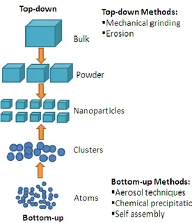
Synthesis approaches and techniques
In order to explore novel physical properties and phenomena and realise potential applications of nanostructures and nanomaterials, the ability to fabricate and process nanomaterials and nanostructures is the first corner stone in nanotechnology. There are two approaches (Figure 1.5) to the synthesis of nanomaterials and the fabrication of nanostructures: down and bottom-up. The top-down approach refers to slicing or successive cutting of a bulk material to get nanosized particles. The bottom-up approach refers to the build-up of a material from the bottom: atom-by-atom, molecule-by-molecule, or cluster-by-cluster. For example, milling is a typical top-down method in making nanoparticles, whereas the colloidal dispersion is a good example of the bottom-up approach in the
24
synthesis of nanoparticles. Both approaches play very important roles in nanotechnology.
25
References
[1] Lane, N. Journal of Nanoparticle Research, 3 (2001) 95. [2] Service R. F., Science, 290 (2000) 1526.
[3] Cohen-Tannoudji, C., Diu, B., Laloe, F., Quantum Mechanics, John Wiley & Sons: New York (2006).
[4] Kittel, C., Introduction to Solid State Physics, 8th edn., R. Oldenbourg Verlag: John Wiley & Sons: New York (2004).
[5] Ashcroft, N. W.; Mermin, N. D., Solid State Physics, Saunders College: Philadelphia (1976).
[6] Davies, J. H.; The Physics of Low-Dimensional Semiconductors; Cambridge University Press: Cambridge (1998).
[7] Moriarty, P., Reports on Progress in Physics (2001), 64, 297. [8] Atkins, P. W., Physical Chemistry; 5th Edn.; Oxford University Press: Oxford (1991).
[9] Karplus, M.; Porter, R. N. Atoms and Molecules, 1st edn. ; W. A. Benjamin, Inc.: New York (1970).
[10] Harrison, W. A., Electronic Structure and the Properties of Solids: The Physics of the Chemical Bond; Dover Publication: Dover (1989).
[11] Kobayashi, A.; Sankey, O. F.; Volz, S. M.; Dow, J. D., Phys. Rev. B, 28 (1983) 935.
[12] Burdett, J. K.; Progress in Solid State Chemistry 15 (1984) 173. [13] Ekimov, A. I.; Onushchenko, A. A. Fiz., Sov. Phys.- Semicond. 16 (1982) 775.
[14] Rossetti, R.; Nakahara, S.; Brus, L. E. J., Chem. Phys. 79 (1983) 1086.
26
[15] (a) Cohen, M. L.; Chou, M. Y.; Knight, W. D.; de Heer, W. A. J. Phys. Chem. 91 (1987) 3141. (b) Wang, C. R. C.; Pollak, S.; Dahlseid, T. A.; Koretsky, G. M.; Kappes, M. J. Phys. Chem. 96 (1992) 7931. (c) Ellert, C.; Schmidt, M.; Schmitt, C.; Reiners, T.; Haberland, H. Phys. Rev. Lett. 75 (1995) 1731.
[16] Murray, C. B.; Norris, D. B.; Bawendi, M. G., J. Am. Chem. Soc. 115 (1993) 8706.
[17] Alivisatos, A. P., Mater. Res. Soc. Bull. 20 (1995) 23.
[18] Shiang, J. J.; Kadavanich, A.; Grubbs, R. K.; Alivisatos, A. P., J. Phys. Chem., (1995), 99 (48).
[19] Ekimov, A. I.; Onushchenko, A. A. Fiz. Tekh. PoluproVodn. 16 (1982) 1215.
[20] Rossetti, R.; Nakahara, S.; Brus, L. E. J. Chem. Phys. 79 (1983) 1086.
[21] Coombes, C. J. J. Phys. 2 (1972) 441.
[22] Buffat, P.; Borel, J.-P. Phys. Rev. A 13 (1976) 2287.
[23] Castro, T.; Reifenberger, R.; Choi, E.; Andres, R. P. Phys. ReV. B:Condens. Matter 42 (1990), 8548.
[24] Beck, R. D.; St. John, P.; Homer, M. L.; Whetten, R. L. Science 253 (1991) 879.
[25] Martin, T. P.; Naher, U.; Schaber, H.; Zimmermann, U. J. Chem.Phys. 100 (1994) 2322.
[26] Couchman, P. R.; Jesser, W. A., Nature, 269 (1977) 481
[27] Ercolessi, F.; Andreoni, W.; Tosatti, E., Phys. Rev. Lett., 66 (1991) 911.
[28] Besson, J. M.; Itie, J. P.; Polian, A.; Weill, G.; Mansot, J. L.; Gonzalez, J. Phys. Rev. B - Condensed Matter 44 (1991) 4214.
27
[29] (a) Chen, C. C.; Herhold, A. B.; Johnson, C. S.; Alivisatos, A. P. Science 276 (1997) 398. (b) Herhold, A. B.; Chen, C. C.; Johnson, C. S.; Tolbert, S. H.; Alivisatos, A. P. Appl. Phys. Lett. 68 (1996) 2574.
[30] (a) Alivisatos, A. P., Phys. Chem. Chem. Phys. 101 (1997) 1573. (b) Alivisatos, A. P., J. Phys. Chem. 100 (1996) 13226.
[31] Gaponenko, S. V. “Optical Properties of Semiconductor Nanocrystals”, Cambridge University Press, 1998.
[32] a) Hodak, J. H.; Henglein, A.; Hartland, G. V. Pure Appl. Chem. 72 (2000) 189. (b) Mulvaney, P. Langmuir 12 (1996) 788. (c) Kamat, P. V. J. Phys. Chem. B 106 (2002) 7729.
[33] (a) Shi, J.; Gider, S.; Babcock, K.; Awschalom, D. D. Science 271 (1996) 937. (b) Billas, I. M; L.; Chatelain, A.; deHeer, W. A. Surf. Rev. Lett. 271 (1996) 937.
28
Catalysis
Introduction
Metal oxides have wide industrial applications in the field of catalysis by serving as active compositions or as supports. There are a lot of opportunities in modifying nanostructures to improve substantially the catalytic activity and selectivity of existing catalysts. Catalysts are species that are capable of directing and accelerating thermodynamically feasible reactions while remaining unaltered at the end of the reaction. They cannot change the thermodynamic equilibrium of reactions [1, 2]. The performance of a catalyst is largely measured in terms of its effects on the reaction kinetics. The catalytic activity is a way of indicating the effect the catalyst has on the reaction rate and can be expressed in terms of the rate of the catalytic reaction, the relative rate of a chemical reaction (i.e. in comparison to the rate of the uncatalysed reaction) or via another parameter, such as the temperature required to achieve a certain conversion after a particular time period under specified conditions. Catalysts may also be evaluated in terms of their effect on the selectivity of a reaction, specifically on their ability to give one particular reaction product. In some cases, catalysts may be used primarily to give high reaction selectivity rather than high conversion rate. Stability is another important catalyst property since catalysts are expected to lose activity and selectivity with prolonged use. This then opens the way to regenerability which is a measure of
29
the catalyst‟s ability to have its activity and/or selectivity restored through some regeneration process. Catalytic processes are the application of catalysts in chemical reactions. In the manufacture of chemicals, catalysis is used to make an enormous range of products, for examples heavy chemicals, commodity chemicals and fine chemicals. Catalytic processes are used throughout fuels processing, in petroleum refining, in synthesis gas conversion, and in coal conversion. More recently, the demand for clean technology or environment protection has driven most of the new developments in catalysis.
Catalysis is described as homogeneous when the catalyst is soluble in the reaction medium and heterogeneous when the catalyst exists in a phase distinctly different from the reaction phase of the reaction medium [3]. Many homogeneous catalytic processes are liquid phase and operate at moderate temperatures (< 150 °C) and pressures (< 20 atm).
Photocatalysis
In 1839 Becquerel [4] reported that a voltage and an electric current were produced when a silver chloride electrode, immersed in an electrolyte solution and connected to a counter electrode, was illuminated with sunlight. It is not usually recognized that many examples of semiconductor photocatalysis had already been reported in the literature by the beginning of the last century. Most notably, the semiconductor ZnO had attracted a great deal of attention at the
30
turn of this century as a photosensitizer for the decomposition of organic compounds [5]. In 1929, it was known that the pigment “titanium white”, namely TiO2, was responsible for fading in paints
[6], and several major studies into sensitized action of TiO2 followed
[7]. During the 1960s, much of the theory of semiconductor photoelectrochemistry was developed, most notably through the contribution of Gerischer [8] and Pleskov and co-workers [9-11].
In 1972, Fujishima and Honda discovered the photocatalytic splitting of water on TiO2 electrodes [12]. This event marked the
beginning of a new era in heterogeneous photocatalysis. Since then, research efforts in understanding the fundamental processes and in enhancing the photocatalytic efficiency of TiO2 have come from
extensive research performed by chemists, physicists, and chemical engineers. In recent years, applications pertaining to environmental cleanup have been one of the most active areas in heterogeneous photocatalysis. This has been inspired by the potential application of semiconductors-based photocatalysts for the total destruction of organic compounds in polluted air and wastewater [13, 14].
In a heterogeneous photocatalytic system, photoinduced molecular transformations or reactions take place at the surface of a catalyst. Depending on where the initial excitation occurs, photocatalysis can be generally divided into two classes of processes. When the initial photoexcitation occurs in an adsorbate molecule which then interacts with the ground state catalyst substrate, the process is referred to as a catalyzed photoreaction. When the initial photoexcitation takes place in the catalyst substrate and the photoexcited catalyst then transfers an electron or energy
31
into a ground state molecule, the process is referred to as a sensitized photoreaction.
Mechanism of photocatalysis
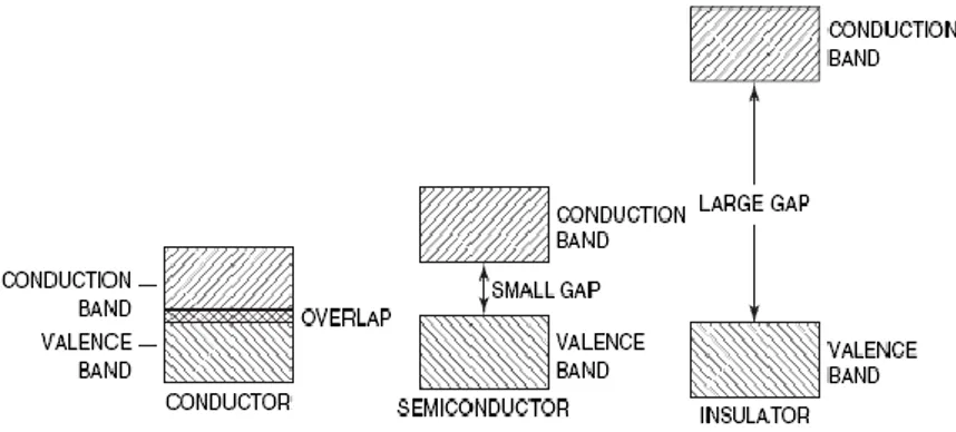
Materials can be divided into 3 different groups, depending of their band gap energies (Fig. 2.1):
Fig. 2.1 Classification of materials depending of their band gap energies
Materials used in photocatalysis are usually metal oxide semiconductors and activation can be done using photons of right energy: the power of semiconductor based photocatalysts, such as TiO2, is due to charge separation ability (Fig. 2.2). When a
nano-semiconductor is illuminated under a light with energy larger than the band gap, an excitation of an electron from the valence band to the conduction band is observed, leaving a hole at the valence band. The separated hole has a strong oxidation power to obtain an electron from the absorbed species. The separated charge and hole can also recombine to release energy in the form of heat.
32
Fig .2.2 Schematic illustration of the charge separation theory of semiconductor
upon a photoexcitation (adapted from ref. [15]).
To enhance the photocatalysis, electron-hole pair recombination must be suppressed. This can be achieved by trapping either the photogenerated electrons or the photogenerated holes at trapping sites in the structure. The band gap of a semiconductor determines its working wavelength. The semiconductors with either too large or too narrow band gaps are not suitable for practical use. The reason is that larger band gap will not cause any reaction while narrow band gap materials will have to face the problem of light erosion. The band gaps of different semiconductors are shown in Figure 2.3. Until now, TiO2 (anatase, band gap ~ 3.2 eV) is the most
extensively studied material for photocatalysts because of its strong oxidizing power, low toxicity, and long-term photostability.
33
Fig. 2.3 Energy diagrams for various semiconductors in aqueous electrolytes at
pH = 1 (adapted from ref. [15]).
The energy that the Earth receives from the Sun is gigantic: 3 ×1024 joules a year, which is about 10,000 times more the energy that the global population currently consumes [16]. In other words, if we could only exploit 0.01 % of this incoming solar energy for the profit of humankind, we could solve the problem of energy shortage. Any improvement in the utilization of sun rays will make a profound positive effect on modern science and technology.
A great deal of effort has been devoted to photoeletrochemical process such as splitting of water [17, 18] and reduction of carbon dioxide for the conversion of solar energy into chemical energy [19, 20]. In addition to applying photocatalysts for energy renewal and energy storage, applications of photocatalysts to environmental cleanup have been one of the most active areas in heterogeneous photocatalysis [21-23].
34
Radical pathways
Once the photogenerated electron-hole pair reaches the catalyst surface in water media (as shown in Figure 2.2), it gives rise to a series of reactions ultimately leading to the formation of hydroxyl radicals. In detail, it is broadly accepted that photogenerated holes (h+) could oxidize H2O or -OH groups present
on the catalyst surface giving rise to hydroxyl radicals (•OH) [23]: Semiconductor (SC) + hν → SC (e- + h+) (1)
h+ + OH- → •OH (2)
h+ + H2O → •OH + H+ (3)
Under ambient atmosphere, molecular oxygen acts as a photogenerated electron (e-) scavenger initiating a series of reactions taking place in aqueous media ultimately yielding •OH group:
O2 + e- → O2•- (4) O2•- + H+ → HO2• (5) HO2• + HO2• → H2O2 + O2 (6) O2•- + HO2• → O2 + HO2- (7) HO2- + H+ → H2O2 (8) H2O2 + hν → 2 •OH (9) H2O2 + O2•- → HO• + OH- + O2 (10) H2O2 + e- → HO• + OH- (11)
35
General applications of photocatalysis
Recent developments in the domain of chemical water treatment have led to an improvement in oxidative degradation procedures for organic compounds dissolved or dispersed in aqueous media, by applying catalytic and photochemical methods. They are generally referred to as Advanced Oxidation Processes (AOP). This domain is particularly oriented towards applications and has already had a strong impact on design and construction of new light sources, photochemical reactors, and the preparation of new photocatalysts and their support. AOP methods exploit the high reactivity of hydroxyl radicals in driving oxidation processes, ultimately resulting in the mineralization of a variety of environmental contaminants. In this field of research, UV-induced photocatalytic degradation assisted by semiconductors represents a very appealing tool to implement low cost purification of waste waters on large scale.
Nanoparticles catalysis
Nanoparticles have attracted a great interest as a subject for scientific research and industrial application under the internationally big research boom of nanoscience and nanotechnology starting from the Clinton‟s statement in 2000 [24], because nanoparticles are easily prepared even in single-nanometer size and their applications to catalysis successfully give the productive results as a fundamental research. However, nanoparticles already had a long history as nanometer-scale materials before the Clinton‟s statement. Soluble gold NPs appeared
36
about two thousand years ago and were used as pigments for aesthetic and curative purposes. On the materials side, their use to make ruby glass and for colouring ceramics was known in these ancient times, as exemplified by the famous Lycurgus cup (dated 4th century B.C., British Museum) [25].
In the history of colloid chemistry, metal nanoparticles, which are called colloidal metal or metal fine particles, have been recognized as a research subject by scientists more than 150 years ago. For example, Michael Faraday reported the preparation of gold sols (colloidal dispersion of gold nanoparticles in water) in 1857 [26], although he could not measure at that time the size of gold nanoparticles. However, the gold nanoparticles he prepared were reproduced by his successor at Royal Institution in London, J. M. Thomas, who demonstrated that the particle size is 3–30 nm in diameter [27].
Nevertheless, nanoparticles in catalysts have a long history too. Human beings had used some materials as a special additive to accelerate practical reactions in history. However, J. J. Berzelius recognized the catalysis as a special phenomenon in 1835 and W. Ostwald gave the definition of catalysis in 1901, when the chemistry of catalysis started practically. Ostwald also defined “colloid” as a dispersion state of materials. Thus, both concepts of “colloid” and “catalysis” had a strong relationship even from the beginning.
One reason of the great reactivity of nanoparticle catalyst can be found in the percentage of “active” atoms, namely those located on the external faces, edges or corners.
37
nanoparticles and the percentage (r/%) of surface atoms in total atoms constructing a nanoparticle. The percentage of surface atoms rapidly increases with decreasing the particle size, especially less than 5 nm. If the diameter is less than 2.5 nm, more than half of the atoms are located at the outermost surface layer of the particle [28].
Figure 2.4 relationship between particle diameter (d/nm) and percentage of
surface atoms in total atoms (r/%).
The corner atoms commonly have the highest number of vacant coordination position among surface atoms. If the activity of the surface atom increases with increasing the number of vacant coordination position, then the catalytic activity of the surface atoms increases in the following order: face < edge < corner. Thus, the increase of the corner atom with decreasing the size could provide the very effective catalyst for such reactions, which we call structure-sensitive reactions.
38
A new concept of nanoparticle catalysts is becoming very popular in science and technology and is going to provide a new frontier in science of material conversion: inorganic catalysts in nanometer scale receive an attention, which gives a new concept of catalysis [28].
39
References
[1] G. Ertl, H. Knozinger, J. Weitkamp, Handbook of Heterogeneous Catalysis, Wiley-VHC, Weinheim (1997).
[2] C. L. Thomas, Catalytic Processes and Proven Catalysts, Academic Press, New York, (1970).
[3] J. M. Thomas, W. J. Thomas, Principles and Practice of Heterogeneous Catalysis, VCH, NY (1996).
[4] Becquerel, E. C.R., Acad. Sci., 9 (1839) 561. [5] Perret, A. J.Chim. Phys., 23 (1926) 97. [6] Keidel, E. Furben Zeitung, 34 (1929) 1242.
[7] Goodeve C.F., Kitchnere, J.A. Trans. Faraday Soc., 34 (1938) 570.
[8] Gerischer, H. Eyring, H., Henderson D., Jost, W. (Eds.) Physical Chemistry – An Advanced Treatise, Academic Press, New York (1970).
[9] Myamlin, V.A. Pleskov, Y. Electrochemistry of Semiconductors, Plenum, New York (1967).
[10] Pleskov, Y.V. Gurevich, Y.Y. Semiconductor
Photoelectrochemistry, Plenum, New York (1986).
[11] Pleskov, Y.V. Solar Energy Conversion, Springer-Verlag, Berlin (1990).
[12] Fujishima, A.; Honda, K., Nature, 37 (1972) 238.
[13] Schiavello, M., Ed. Photocatalysis and Environment; Kluwer Academic Publishers: Dordrecht (1988).
40
[14] Ollis, D. F., Al-Ekabi, H., Eds. Photocatalytic Purification and Treatment of Water and Air, Elsevier: Amsterdam (1993).
[15] A. L. Linsebigler, G. Q. Lu, J. T. Yates, Chem. Rev., 95 (1995), 735-758.
[16] M. Grätzel, Nature, 414 (2001) 338-344.
[17] M. Ni, M. K. H. Leung, D. Y. C. Leung, K. Sumathy, Renew. Sust. Energy Rev. 11 (2007) 401-425.
[18] Z. G. Zou, J. H. Ye, K. Sayama, H. Arakawa, Nature, 414 (2001) 625-627.
[19] K. Koci, L. Obalova, L. Matejova, D. Placha, Z. Lacny, J. Jirkovsky, O. Solcova, Appl. Catal. B, 89 (2009) 494-502.
[20] H. Yamashita, H. Nishiguchi, N. Kamada, M. Anpo, Y. Teraoka, H. Hatano, S. Ehara, K. Kikui, L. Palmisano, A. Sclafani, M. Schiavello, M. A. Fox, Res. Chem. Intermed., 20 (1994) 815-823.
[21] M. R. Hoffmann, S. T. Martin, W. Y. Choi, D. W. Bahnemann, Chem. Rev., 95 (1995) 69-96.
[22] M. I. Litter, Appl. Catal. B, 23 (1999) 89-114.
[23] M. A. Fox, M. T. Dulay, Chem. Rev., 93 (1993) 341-357. [24]
http://en.wikipedia.org/wiki/National_Nanotechnology_Initiative http://marcomm.caltech.edu/events/presidential_speech/pspeechtxt.h tml
[25] M. C. Daniel, D. Astruc, Chem. Rev., 104, (2004), 293. [26] M. Faraday, Phil. Trans. Roy. Soc., 147, (1857), 145–181. [27] J. M. Thomas, Pure Appl. Chem., 60, (1988), 1517–1527. [28] N. Toshima, “Inorganic Nanoparticles for Catalysis” in
41
“Inorganic Nanoparticles: Synthesis, Applications, and Perspectives” edited by C. Altavilla and E. Ciliberto, Taylor and Francis Group, 2011.
42
Titanium Dioxide
Introduction
Titanium is the world‟s fourth most abundant metal and ninth most abundant element. It was discovered in 1791 in England by Reverend William Gregor, who recognised the presence of a new element in ilmenite. It was then rediscovered in rutile ore several years later by a German chemist, Heinrich Klaporth who named it after Titans, mythological sons of goddess “Gaia” (earth in Greek mythology). Titanium is not found in its elemental state, it occurs mainly in minerals like rutile, ilmenite, leucoxene, anatase, brookite, and perovskite. It is also found in titanates and many iron ores.
Figure 3.1 shows the 3 main natural phases of TiO2: anatase
(tetragonal), rutile (tetragonal), and brookite (orthorhombic):
Anatase (A) Rutile (B) Brookite (C)
Fig. 3.1 Elemental unit cells of anatase (A), rutile (B) and brookite (C)
At lower temperatures the anatase and brookite phases are more stable, but both will revert to the rutile phase when subjected to high
43
temperatures. Although rutile is the most abundant of the three phases, many quarries and mines containing only the anatase or brookite form exist. The optical properties of each phase are also similar, however there is a slight difference among them. For photocatalytic processes, anatase is the preferred structure, although all three forms have shown to be active.
Anatase and brookite are metastable phases and they transform to rutile in the range of 973K – 1173K (Figure 3.2). The anatase to rutile transformation (ART) temperature depends on purity, type of impurities, particle shape/size, atmosphere and reaction conditions. Reidy et al. [1] discussed the role of the critical particle size i.e. about 45 nm as a main parameter of ART irrespective of the purity and the type of impurity in the anatase. The size dependence of the ATR is related to the surface free energy, which is lower for anatase than that of rutile, which is the reverse of the bulk situation [1, 2]. Rutile, due to its thermodynamical stability is the most extensively studied among all TiO2 forms. In the anatase
and rutile structures, each titanium ion is in the centre of an oxygen octahedron, but in rutile the oxygen ions form a slightly distorted hexagonal compact lattice and in anatase form a cfc lattice (Fig. 3.1). In both structures, each oxygen ion is coplanar near neighbour titanium cations. The three Ti-O-Ti angles are roughly equal to 120° in rutile. On the other hand, in anatase one Ti-O-Ti angle is about 180° while the other two are close to 90°. The various Ti-O-Ti angle values result in a significant widening of the d bands with an accompanying decrease in effective mass and an increase in
44
mobility. Basic crystallographic properties [3, 4] of titanium dioxide are listed below:
Table 3.1 Titanium dioxide properties
Property Anatase Rutile Brookite
Melting point (°C) ~ 1825 ~ 1825 ~ 1825
Boiling Point (°C) 2500 ~ 3000 2500 ~ 3000 2500 ~ 3000
Crystallographic structure Tetragonal Tetragonal Orthorhombic
Space group I41/amd P42/mmm Pcab
Lattice parameters (nm) a = 0.3784 b = 0.9515 a = 0.4594 c = 0.2959 a = 0.5442 b = 0.9168 Unit cell volume
[10-3 nm3] 34.172 31.216 32.567
Density at 298 K (g/cm3) 4.230 4.250 4.133
Band gap energy (eV) 3.20 3.03 2.99
Other information can be obtained from phase diagrams of polymorphic forms [5, 6]:
45
TiO2 in Anatase metastable phase
The anatase polymorph of TiO2 is one of its two metastable
phases together with brookite phase. For calcination processes above 700 °C all anatase structure becomes rutile. Some authors also found that 500 °C would be enough for phase transition from anatase to rutile when thermal treatment takes place. Anatase structure is tetragonal, with two TiO2 formula units (six atoms) per primitive
cell. Lattice parameters are: a = b = 3.7710 Å and c = 9.430 Å with c/a ratio of 2.5134.
TiO2 in Rutile stable phase
TiO2 owing to its chemical and mechanical stabilities,
titanium dioxide (TiO2), which is a wide energy gap n-type
semiconductor, has been mainly used to develop gas sensors based in thick film polycrystalline material or small particles. Its unit cell contains Ti atoms occupy the centre of a surrounding core composed of six oxygen atoms placed approximately at the corners of a quasi-regular octahedron. The lattice parameters correspond now to a = b = 4.5933 Å and c = 2.9592 Å with c/a ratio of 0.6442.
TiO2 in Brookite phase
Brookite was first discovered in 1849 in Magnet Cove, a site of large deposits of the mineral. It was originally dubbed “arkansite” for the state it was discovered in Arkansas. The brookite structure is more complicated and has a larger cell volume than the other two forms. It is also the least dense of the three forms. The unit cell is
46
composed of eight formula units of TiO2 and is formed by edge
sharing TiO2 octahedra, similar to rutile and anatase. Brookite
belongs to the orthorhombic crystal system and its space group is Pbca. By definition, the brookite structure is of lower symmetry than its TiO2 counter morphs, the dimensions of the unit cell are unequal.
Also the Ti-O bond lengths vary more in the rutile or anatase phases, like the O-Ti-O bond angles do.
Depending of the stoichiometry, pressure and temperature, other possible forms can exist [6], as shown in Fig. 3.3:
Fig. 3.3 TiO2 phase diagram (temperature versus composition)
For example, two new high pressure forms, a monoclinic baddeleyite-like form and an orthorhombic α-PbO2-like form, both
47
TiO
2as nano-photocatalyst
Among all the oxide semiconductors that have been examined, titanium dioxide (TiO2) is the most studied due to its
excellent photocatalytic properties and availability.
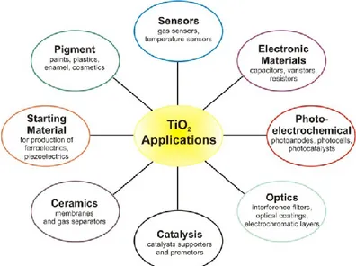
It is utilized in a range of fields such as: solar cells, photoelectrochemistry, photocatalyst for environmental applications, semiconductor (i.e. gas application), self clean-up surfaces (for its hydrophilic and hydrophobic properties in the absence or in the presence of UV-Vis light), with many applications in everyday life: white pigments, cements, papers, beauty creams, food additives, etc, and recently also as killing bacteria agent [9]:
Fig. 3.4 Applications of TiO2
Many good reviews [10-12] and books [13, 14] have been written on this photocatalyst; TiO2, in its anatase form, possesses
48
desirable properties for applications in homogenous and heterogeneous catalysis such as:
high surface area; limited toxicity;
high availability & low cost;
excellent thermal and photochemical stability; water insolubility & photocatalyst recyclability;
no expensive and dangerous oxidizing chemicals such as O3 or H2O2 (dissolved oxygen or air is sufficient) are
used;
free light source (solar light).
In its rutile form, the TiO2 photocatalytic ability is greatly
reduced [15-17].
Photocatalytic reactions on TiO2 surfaces are very important
for environmental removal of both air pollutants and water purification, such as the oxidation of organic and inorganic pollutants (HCHO, NOx, etc) and the reduction of heavy metals;
moreover complete mineralization of a wide variety of organic compounds to CO2 and H2O has been reported [18-21].
Electron – hole pairs are formed when TiO2 is irradiated with
photons of greater energy than its band gap (3.2 eV for pure anatase):
49
Electrons are promoted from the valence band to the conduction band: thus the conduction band acts as a reduction zone and conversely the valence band as an oxidation zone.
Due to its possible applications, many studies have been carried out on the anatase TiO2 nanoparticles (the phase showing the
best photocatalytic performance) to understand better its electronic structure, as well as chemical and physical properties [22].
The properties of nano-sized semiconductor particles have been known to be very sensitively related to the particle size: nano-scaling of materials has opened up a new dimension exhibiting unique physical and chemical properties which correspond neither to those of atoms and molecules nor to the bulk materials, with identical chemical composition [23].
Chemical, electrical and structural properties of nano-crystalline materials are of great interest today, as it is important to obtain materials with high specific area and quantum size effects especially in the field of catalysis. With a decrease in particle size of TiO2 to the nanometer scale, the catalytic activity is enhanced as the
optical band gap is widened resulting from the quantum size effect, combined with the increased surface area [24]. Precise control of the size of semi-conducting oxide materials at the nanometric scale is of absolute importance for fine-tuning their photocatalytic properties. Unfortunately nanoparticles show a tendency to aggregate, due to their high surface area-to-volume ratio, which may impede their application [25].