Journal of Physics: Conference Series
OPEN ACCESS
Towards an Electronic Interferometer based on
Spin-Resolved Quantum Hall Edge States
To cite this article: B Karmakar et al 2013 J. Phys.: Conf. Ser. 456 012019
View the article online for updates and enhancements.
Related content
Coherent control of single electrons: a review of current progress
Christopher Bäuerle, D Christian Glattli, Tristan Meunier et al.
-Effect of an in-plane magnetic field on microwave photoresistance and Shubnikov-de Haas effect in high-mobility GaAs/AlGaAs quantum wells
A Bogan, A T Hatke, S A Studenikin et al.
-Nonequilibrium currents in the quantum Hall effect regime spatially resolved by transport experiment
M V Budantsev, A G Pogosov, D A Pokhabov et al.
-Recent citations
Time-dependent simulation and analytical modelling of electronic Mach–Zehnder interferometry with edge-states wave packets
Andrea Beggi et al
Towards an Electronic Interferometer based on
Spin-Resolved Quantum Hall Edge States
B. Karmakar1,*, D. Venturelli1, L. Chirolli1, F. Taddei1, V. Giovannetti1, R.
Fazio1, S. Roddaro1, G. Biasiol2, L. Sorba1, L. N. Pfeiffer3, K. W. West3, V.
Pellegrini1 and F. Beltram1
1NEST, Scuola Normale Superiore and Instituto Nanoscienrze-CNR, Pisa, Italy 2Istituto Officina dei Materiali CNR, Laboratorio TASC, Basovizza (TS), Italy 3School of Engineering and Applied Science, Princeton University, New Jersey, USA
Abstract. Spin resolved edge states are ideal candidates for the implementation of dual-rail quantum computation architectures by encoding the qubit in the spin degree of freedom of the co-propagating edge states. An important element for the realization of such architectures is a coherent beam splitter that controllably mixes the two co-propagating spin-resolved edge channels. Coupling of the spin resolved edge states is demonstrated recently by spin-flip scattering event that is induced by in-plane spatially-dependent periodic magnetic field of the nano-magnet array placed at the boundary of the mesa. In this paper we discuss the nanofabrication and our preliminary transport analysis of an electronic interferometer device made of two nano-magnetic arrays placed in close proximity. The impact of temperature in the coherent properties of the devices is addressed.
1. Introduction
Observation of quantum interference effect in electronic Mach-Zehnder interferometer (MZI) using counter propagating quantum Hall (QH) edge channels1 proved that coherent QH edge channel circuit
is a promising solid state system for quantum information processing. Very large visibility ~62% of the quantum interference in MZI is the signature of long coherence length1 of the QH edge channels at
low temperature ~10mK. The edge channels are orthogonal Eigen states and they are immune to impurity scattering and geometrical defects2. As a result, the edge channels are topologically protected
that is characterized by a bulk insulating gap3 created under application of a high magnetic field B on a
two dimensional electron gas (2DEG). Based on these promising properties of the QH edge states, various coherent electronic circuits have been investigated4,5,6.
Implementation of dual-rail7 quantum computation architectures8 by encoding the qubit in the two
distinct co-propagating energy-degenerate orthogonal QH edge states is very promising for testing quantum algorithms. A key element for the realization of such architectures8,9,10 is a coherent beam
splitter that makes it possible to prepare any superposition of the two logic states, thus realizing one-qubit gate transformations. Recently we have demonstrated resonant coupling11 of the spin resolved
edge states (SRESs) at filling factor ν = 2 (number of filled Landau level) by spin-flip scattering events that is induced by in-plane spetially-dependent periodic magnetic field of the nano-magnet
HMF-20 IOP Publishing
array placed at the boundary of the mesa. In this paper we introduce an electronic interferometer device based on such resonant nano-magnetic coupling of the SRESs and present initial characterization of the device down to T = 250mK.
2. Dual-rail architecture
The dual-rail architectures8 proposed by Giovannetti et al. are analogues to linear quantum optics
architectures12,13 for quantum information processing. The proposed architectures are based on
coherent electronic transport in the topologically protected QH edge states, where superposition of states are formed by coherent beam mixing of the two orthogonal edge states and flying qubit gate transformation is performed by inducing Aharonov–Bohm flux in the circuit. The main advantage of this architecture8 is the availability of the two beams after qubit transformation for further processing.
On top of that the devices will suffer less flux instability due to small Aharonov–Bohm loop area defined by a small metal gate (see fig.1) in the circuit. In this topologically protected edge channel circuit quantum information is preserved and does not interact with the environment. Moreover, development of single electron source14 for single electron interferometer circuits is easy because of
Fermionic nature of the electrons. Importantly, the proposed architecture entirely relies on the coherent mixing of the two edge channels. Recently, controlled coupling11 of the SRESs was
demonstrated by our group by triggering a resonant charge transfer by spin-flip events with a magnet array placed at the boundary of the mesa. Based on the exploitation of this resonant nano-magnetic coupling, our further aim is to investigate an electronic interferometer following dual-rail architectures8.
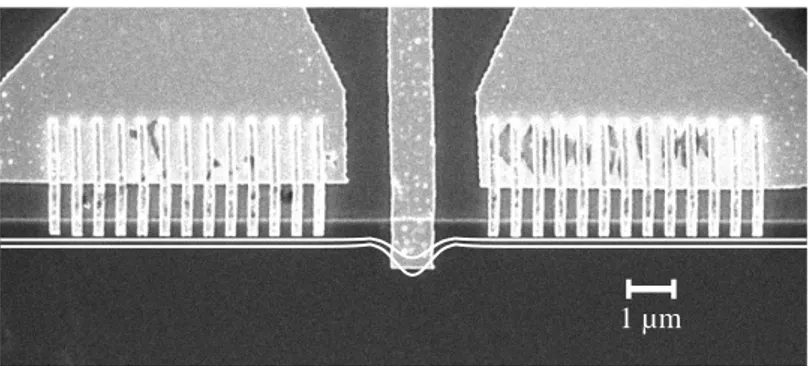
Figure 1: SEM micrograph of the interferometer device with nano-magnet array of periodicity λ =
500nm. Two sets of nano-magnet arrays are used as beam mixer and the metal gate at the middle opens up the loop for inducing Aharonov–Bohm flux under application of a negative voltage bias on it. Two white lines schematically represent SRESs.
3. Device fabrication
The interferometric device is fabricated on a one-sided modulation-doped AlGaAs/GaAs heterostructure grown by molecular beam epitaxy. The 2DEG resides at the AlGaAs/GaAs hetero-interface located 100 nm below the top surface. A spacer layer of 42 nm separates the 2DEG from the Si δ-doping layer above it. The 2DEG has nominal electron density of 1.3 × 10¹¹/cm2 and
low-temperature mobility nearly 4 × 106cm2/V-s. The mesa is defined by e-beam lithography and wet
chemical etching. Ohmic contacts to the mesa are defined by photolithography, thermal evaporation of Ni/Au-Ge/Au and then rapid thermal annealing. The Cobalt nano-magnet arrays of periodicity λ = 500nm are defined at the mesa boundary of the 2DEG using e-beam lithography and thermal evaporation of 10nm Ti followed by 140nm Co and 10nm Au. Evaporation of Ti enhances adhesion of Co and removes remnant O2 from the evaporation chamber and top 10nm Au protects forming of CoO,
which is anti-ferromagnetic in nature. The nano-magnet arrays have overlap on the mesa of about 300nm and are extended over 6.2μm along the mesa boundary. For inducing Aharonov–Bohm flux a metal gate in between the two nano-magnet arrays (fig.1) is defined by e-beam lithography and
1 µm
I
1 µmI
HMF-20 IOP Publishing
Journal of Physics: Conference Series 456 (2013) 012019 doi:10.1088/1742-6596/456/1/012019
thermal evaporation of 10nm Ti and 150nm of Au. The SRESs are separately contacted at the source and drain sides (not shown in fig.1) by suitable metal gating near the Ohmic contacts (see ref.[11]).
Figure 2: (Color online) Plot of the transmitted spin up (↑) and spin down (↓) edge channel current
with the nano-magnet voltage Va for the two left and right arrays. The working magnetic field B =
2.6T is chosen nearly at the center of the ν = 2 plateau. The spin up edge channel is excited with a voltage bias of 25.8μV. Spin-flip process enhances the current in the spin down channel and decreases spin up channel current, while the total current remain constant nearly 1nA.
Figure 3: (Color online) Plot of the transmitted spin up (↑) and spin down (↓) edge channel current
with the nano-magnet voltage Va for the right array at different magnetic field B within the ν = 2
plateau. The multiple resonant peaks move towards higher voltage bias Va with increasing magnetic
field B.
4. Experimental results
At the beginning of the experiments, the working points like magnetic field B, gate voltage for separately contacting the edge channels etc. are needed to set in the device. At first a two-terminal magneto-current (2TMR) measurement (see ref.[11]) is carried out at temperature T = 250mK with a voltage excitation of 25.8µV in one terminal while monitoring the transmitted current in the other terminal. From the 2TMR measurement, the extension of the ν = 2 plateau is found out in the magnetic field range from 2.45T to 2.75T. To separately contacting the SRESs (see ref.[11]), a voltage bias Vg =
0.068V is found out to be suitable on the metal gates near the Ohmic contacts in this device. Then the nano-magnetic coupling is tested in the interferometer device (fig.1) by changing the voltage bias Va
HMF-20 IOP Publishing
on the nano-magnet arrays. The traces of the voltage Va dependence of the transmitted spin up (↑) and
spin down (↓) edge channel currents at a magnetic field of B = 2.6T are plotted in fig.2. At large negative bias Va = -1V on both the arrays, where the nano-magnetic coupling is expected to be
negligible, we see a spin-mixing of nearly 20%. On top of this inherent spin-mixing (as background), an enhancement of spin-mixing of about 10% is observed for both the arrays at resonance with low applied voltage bias Va nearly at -0.22V and -0.27V. The voltage bias Va at the resonant spin-mixing
for the two arrays are found to be little different, probably due to difference in local electrostatic conditions.
In fig.3 the traces of the nano-magnet voltage Va dependence of the transmitted spin up (↑) and spin
down (↓) edge channel current at different magnetic fields B within the ν = 2 plateau are plotted for the right array. The multiple resonance peaks move towards higher voltage Va of the nano-magnet array
with increasing magnetic field B. We note that such a behavior was already seen in our previous work11. It should be also stressed that the inherent background mixing also reduces with increasing
magnetic field, but does not become negligible. This inherent background spin-mixing15 suggests an
incoherent spin-mixing process in the system, which might prevent quantum interference oscillation in the device. Indeed, quantum interference oscillation is not observed in the device at the lowest available temperature 250mK.
Figure 4: (Color online) Temperature dependence of the spin-resolved edge channel current at
magnetic field B = 2.62T with nano-magnet voltage bias Va = -1V. SRESs completely relax over the
copropagating length of 100µm by thermally activated spin-flip process above temperature 0.7K.
Temperature dependence of the spin-resolved edge channel current at magnetic filed B = 2.62T is plotted in fig.4. In this experiment, the nano-magnet voltage bias is kept at Va = -1V, such that the
edge channels are deflected far away from the nano-magnet arrays and the nano-magnetic coupling become negligible. In this condition, thermally activated spin-relaxation processes completely equilibrate the SRESs over the copropagating distance of 100µm above temperature 0.7K. This experiment is carried out at a magnetic field B = 2.62T at filling factor ν = 2, where the Zeeman gap is nearly Ez = 0.064meV (0.8K). We believe that such a low Zeeman gap Ez is responsible for the
significant spin-relaxation observed at the temperature 250mK. The evolution of the experimental curves in fig.4 suggests that the spin-relaxation can be further suppressed by lowering the sample temperature below 250mK.
5. Discussions
In this low-density 2DEG, resonant nano-magnetic coupling is observed on top of the thermally activated spin-relaxation process. The behavior of the resonant coupling by changing the magnetic field B within the ν = 2 plateau is similar to our previous work11. The resonant coupling is not
HMF-20 IOP Publishing
Journal of Physics: Conference Series 456 (2013) 012019 doi:10.1088/1742-6596/456/1/012019
sufficient to observe the quantum interference oscillation in the device at the available temperature of 250mK. At this temperature coexisting thermally-activated spin-relaxation incoherent processes take place over the co-propagating distances. Therefore, suppression of the thermally activated spin-relaxation events is a key requirement and that can be reached by further lowering the sample temperature. After achieving the suppression of such incoherent processes at low temperature, the coherence of the resonant nano-magnetic coupling can be tested. We plan to carry out such experiments in the near future by using a dilution fridge with a base temperature of 10mK.
6. Conclusions
Resonant nano-magnetic coupling is observed in a low-density sample (ns = 1.3×10¹¹/cm2) with a
nano-magnet periodicity of λ = 500nm at a temperature of 250mK on top of a thermally activated spin-relaxation background. The existence of such incoherent spin-spin-relaxation processes is detrimental to the expected coherent behavior of our device. Suppression of the thermally activated spin-relaxation process is an essential step to observe the coherent transport in our interferometric device. This condition can be reached at dilution fridge temperatures.
7. Acknowledgement
This work was supported by MIUR through FIRBIDEAS Project No. RBID08B3FM and by EU through Projects SOLID and NANOCTM.
References
[1] Y. Ji et al., Nature (London) 422, 415 (2003).
[2] B. I. Halperin, Phys. Rev. B 25, 2185 (1982); M. Bu¨ttiker, Phys. Rev. B 46, 12 485 (1992).
[3] C. L. Kane and E. J. Mele, Phys. Rev. Lett. 95, 226801 (2005); B.A. Bernevig, T. L. Hughes, and S. C. Zhang, Science 314, 1757 (2006); D. Hsieh et al., Nature (London) 452, 970 (2008); S. Das Sarma, M. Freedman, and C. Nayak, Phys. Rev. Lett. 94, 166802 (2005).
[4] I. Neder et al., Nature (London) 448, 333 (2007); Phys. Rev. Lett. 96, 016804 (2006); Phys. Rev. Lett. 98, 036803 (2007).
[5] P. Roulleau et al., Phys. Rev. B 76, 161309(R) (2007); Phys. Rev. Lett., 100, 126802 (2008); Phys. Rev. Lett., 102, 236802 (2009). E. Bieri et al., Phys. Rev. B 79, 245324 (2009). S. Roddaro et al., Phys. Rev. Lett. 103, 016802 (2009).
[6] R. L. Willett, L. N. Pfeiffer and K. W. West., PNAS 106, 8853 (2009).
[7] Isaac L. Chuang and Yoshihisa Yamamoto. Phys. Rev. A 52, 3489–3496 (1995). [8] V. Giovannetti, F. Taddei, D. Frustaglia, and R. Fazio, Phys. Rev. B 77, 155320 (2008). [9] T. M. Stace, C. H.W. Barnes, and G. J. Milburn, Phys. Rev. Lett. 93, 126804 (2004). [10] C. Nayak et al., Rev. Mod. Phys. 80, 1083 (2008).
[11] B. Karmakar et al., Phys. Rev. Lett. 107, 236804 (2011).
[12] E. Knill, R. Laflamme and G. J. Milburn. Nature 409, 46 (2001).
[13] Alberto Politi, Martin J. Cryan, John G. Rarity, Siyuan Yu and Jeremy L. O’Brien. Science 320, 646 (2008); Jonathan C. F. Matthews, Alberto Politi, Andre´ Stefanov and Jeremy L. O’Brien. Nature Photonics 3, 346 (2009).
[14] G. Feve, et al., Science 316, 1169-1172 (2007).
[15] G. Muller et al., Phys. Rev. B 45, 3932 (1992); S. Komiyama, H. Hirai, M. Ohsawa, and Y. Matsuda, Phys. Rev. B. 45, 11085 (1992).
HMF-20 IOP Publishing