U
NIVERSITÀ DEGLI
S
TUDI DI
N
APOLI
F
EDERICO
II
P
H
.D.
THESIS
IN
I
NFORMATION
T
ECHNOLOGY AND
E
LECTRICAL
E
NGINEERING
A
R
ECONFIGURABLE AND
E
XTENSIBLE
E
XPLORATION
P
LATFORM FOR
F
UTURE
H
ETEROGENEOUS
S
YSTEMS
M
IRKO
G
AGLIARDI
T
UTOR:
P
ROF.
A
LESSANDROC
ILARDOCOORDINATOR:PROF.DANIELE RICCIO
XXXI
C
ICLOSCUOLA POLITECNICA E DELLE SCIENZE DI BASE
Accelerator-based –or heterogeneous– computing has become increasingly important in a variety of scenarios, ranging from High-Performance Com-puting (HPC) to embedded systems. While most solutions use sometimes custom-made components, most of today’s systems rely on commodity high-end CPUs and/or GPU devices, which deliver adequate performance while ensuring programmability, productivity, and application portability. Unfor-tunately, pure general-purpose hardware is affected by inherently limited power-efficiency, that is, low GFLOPS-per-Watt, now considered as a pri-mary metric. The many-core model and architectural customization can play here a key role, as they enable unprecedented levels of power-efficiency compared to CPUs/GPUs. However, such paradigms are still immature and deeper exploration is indispensable.
This dissertation investigates customizability and proposes novel solutions for heterogeneous architectures, focusing on mechanisms related to coher-ence and network-on-chip (NoC). First, the work presents a non-coherent scratchpad memory with a configurable bank remapping system to reduce bank conflicts. The experimental results show the benefits of both using a customizable hardware bank remapping function and non-coherent memo-ries for some types of algorithms. Next, we demonstrate how a distributed synchronization master better suits many-cores than standard centralized solutions. This solution, inspired by the directory-based coherence mech-anism, supports concurrent synchronizations without relying on memory transactions. The results collected for different NoC sizes provided indica-tions about the area overheads incurred by our solution and demonstrated the benefits of using a dedicated hardware synchronization support. Fi-nally, this dissertation proposes an advanced coherence subsystem, based on the sparse directory approach, with a selective coherence maintenance system which allows coherence to be deactivated for blocks that do not re-quire it. Experimental results show that the use of a hybrid coherent and non-coherent architectural mechanism along with an extended coherence protocol can enhance performance.
The above results were all collected by means of a modular and customiz-able heterogeneous many-core system developed to support the exploration of power-efficient high-performance computing architectures. The system is based on a NoC and a customizable GPU-like accelerator core, as well as a reconfigurable coherence subsystem, ensuring application-specific config-uration capabilities. All the explored solutions were evaluated on this real
heterogeneous system, which comes along with the above methodological results as part of the contribution in this dissertation. In fact, as a key benefit, the experimental platform enables users to integrate novel hard-ware/software solutions on a full-system scale, whereas existing platforms do not always support a comprehensive heterogeneous architecture explo-ration.
The results and research activities presented in this dissertation have been published in scientific conferences or journals during my Ph.D studentship: • Cilardo, A., Flich, J., Gagliardi, M. and Gavila, R.T., 2015, Au-gust. Customizable heterogeneous acceleration for tomorrow’s high-performance computing. In High Performance Computing and Com-munications (HPCC), 2015 IEEE 7th International Symposium on Cyberspace Safety and Security (CSS), 2015 IEEE 12th International Conferen on Embedded Software and Systems (ICESS), 2015 IEEE 17th International Conference.
• Cilardo, A., Gagliardi, M. and Donnarumma, C., 2016, November. A Configurable Shared Scratchpad Memory for GPU-like Processors. In International Conference on P2P, Parallel, Grid, Cloud and Internet Computing.
• Cilardo, A., Gagliardi, M. and Passaretti, D., 2017, November. NoC-Based Thread Synchronization in a Custom Manycore System. In International Conference on P2P, Parallel, Grid, Cloud and Internet Computing.
• Gagliardi, M., Fusella, E. and Cilardo, A., 2018, July. Improving Deep Learning with a customizable GPU-like FPGA-based accelerator. In 2018 14th Conference on Ph. D. Research in Microelectronics and Electronics (PRIME).
• Zoni, D., Cremona, L., Cilardo, A., Gagliardi, M. and Fornaciari, W., 2018. PowerTap: All-digital power meter modeling for run-time power monitoring. Microprocessors and Microsystems.
• Cilardo, A., Gagliardi, M., Scotti, V. Lightweight hardware support for selective coherence in heterogeneous manycore accelerators. In 2019 Conference on Design, Automation ans Test (DATE). Ongoing peer review.
1 Introduction 1
1.1 Methodology . . . 4
1.2 Thesis Structure . . . 4
2 Technical Background 6 2.1 Parallelism in CPU and the ILP Wall . . . 6
2.1.1 Very Long Instruction Word . . . 7
2.1.2 Multiprocessor and Thread-Level Parallelism . . . 8
2.2 Computational Intense Accelerators: GPUs . . . 9
2.2.1 GPU Architecture . . . 11
2.2.2 GPU Programming Model . . . 11
2.2.3 NVIDIA Architecture . . . 12
2.2.4 The Programming Model . . . 13
2.3 Heterogeneous Computing in HPC . . . 15
2.4 Open-source and FPGA-based Accelerators . . . 15
2.5 Network-on-chips . . . 17
2.5.1 Real on-chip Networks . . . 18
2.6 Cache Coherence . . . 19
2.6.1 Incoherence Issues . . . 19
2.6.2 Coherence States . . . 21
2.6.3 Coherence Transactions . . . 23
2.6.4 Snooping . . . 24
3 Baseline Many-Core Exploration Platform 26 3.1 Tile Overview . . . 27
3.2 Design principles . . . 28
3.3 Core microarchitecture . . . 28
3.4 Networking System . . . 36
3.4.2 Network Interface . . . 38
4 Configurable Coherence Subsystem 40 4.1 Cache Hierarchy . . . 40 4.1.1 Architectural Details . . . 41 4.2 Load/Store unit . . . 42 4.3 Cache Controller . . . 45 4.3.1 Stage 1 . . . 46 4.3.2 Stage 2 . . . 47 4.3.3 Stage 3 . . . 48 4.3.4 Stage 4 . . . 48 4.3.5 Protocol ROM . . . 49 4.4 Directory Controller . . . 49 4.4.1 Stage 1 . . . 50 4.4.2 TSHR Signals . . . 51 4.4.3 Stage 2 . . . 51 4.4.4 Stage 3 . . . 51 4.4.5 Protocol ROM . . . 51 5 Exploring Customization 53 5.1 Motivations . . . 53 5.2 Related Works . . . 54 5.3 Convolutional Layer . . . 54 5.4 Evaluation . . . 56 5.5 Conclusions . . . 59
6 Customizable Shared Scratchpad Memory 60 6.1 Motivations . . . 60
6.2 Related Works . . . 61
6.3 Architecture . . . 62
6.3.1 SPM interface and operations . . . 63
6.3.2 Remapping . . . 64
6.3.3 Implementation details . . . 65
6.3.4 Integration consideration in the baseline GPU-like core 66 6.4 Evaluation . . . 67
6.4.1 Methodology . . . 67
6.4.2 Kernels . . . 67
6.4.2.1 Matrix Multiplication . . . 67
6.4.2.2 Image Mean Filter 5 × 5 . . . 68
7 Distributed Thread Synchronization 71
7.1 Motivations . . . 71
7.2 Related Works . . . 73
7.3 Centralized solution vs distributed synchronization master . . 74
7.4 Architecture . . . 76 7.4.1 Barrier Core . . . 77 7.4.2 Synchronization Core . . . 78 7.4.3 An example of synchronization . . . 79 7.5 Implementation . . . 80 7.6 Evaluation . . . 82 7.6.1 Simulation . . . 82 7.7 Conclusions . . . 85
8 Selective coherence in many-core accelerators 86 8.1 Motivations . . . 86
8.2 Related Works . . . 88
8.3 Proposed solution . . . 90
8.3.1 Networking Infrastructure and Synchronization Support 90 8.3.2 Accelerators . . . 91
8.3.3 Coherence sub-system . . . 91
8.3.4 Selective coherence deactivation . . . 93
8.3.5 Extended MSI protocol . . . 94
8.4 Experimental evaluation . . . 96
8.4.1 Implementation Overhead . . . 98
8.5 Conclusions . . . 98
Conclusion 101
2-1 Superscalar, fine MT, coarse MT and SMT (credits [39]) . . . 8
2-2 CPU vs GPU . . . 10
2-3 Architecture of a modern GPU (credits NVIDIA) . . . 11
2-4 Shifting from multi-core to heterogeneous systems. . . 14
3-1 The nu+ many-core overview. . . 27
3-2 Overview of the core microarchitecture . . . 28
3-3 Baseline hardware router. . . 37
3-4 Overview of the Network Interface design. . . 38
4-1 The nu+ coherence sub-system overview. . . 41
4-2 Load/store unit detailed view. . . 42
4-3 Cache Controller overview. . . 45
4-4 MSHR entry overview. . . 47
4-5 Default MSI protocol implemented at the Cache Controller level. . . 49
4-6 Directory Controller overview. . . 50
4-7 TSHR entry. . . 51
4-8 Default MSI protocol on the directory side. . . 52
5-1 Speedup over naive scalar single-thread implementation on 16 × 16, 32 × 32, and 64 × 64 input images with 3 × 3, 5 × 5, and 7 × 7 filter kernels. . . 56
5-2 Speedup over single-thread implementation when varying the number of threads on 16×16, 32×32, and 64×64 input images with 3 × 3, 5 × 5, and 7 × 7 filter kernels. . . 57
5-3 The speedup achieved using scratchpad memory when vary-ing the number of threads on 16 × 16, 32 × 32, and 64 × 64 input images with 3 × 3, 5 × 5, and 7 × 7 filter kernels. . . 58
6-1 High-level generic GPU-like core with scratchpad memory. . . 62
6-2 SPM design overview. . . 63
6-3 This figure shows how addresses are mapped onto the banks. Takes into account that the memory is byte addressable and that each word is four byte. In the case of generalized cyclic mapping the remapping factor is 1. . . 64
6-4 LUTs and FFs occupation of the FPGA-based SPM design for a variable number of banks . . . 65
6-5 LUTs and FFs occupation of the FPGA-based SPM design for a variable number of lanes . . . 66
7-1 Typical many-core mesh-based with 64 tiles . . . 74
7-2 Simplified execution flow and synchronization points. . . 75
7-3 FSM of Barrier Core. . . 78
7-4 Overview of the Synchronization Core. . . 79
7-5 Synchronization messages, 64 bits each. The Account mes-sage is sent to the master, when a thread hits the barrier from the core side. The Release message is sent by the synchro-nization master to all the involved cores when all the Account messages are collected. . . 80
7-6 Example of barrier synchronization . . . 81
8-1 Detail of a processing tile in the proposed solution for hetero-geneous systems. This figure highlights the Cache Controller and the extension for noncoherent region support. The CC mainly relies on the distributed directory, on an extended coherence protocol which resides in its embedded protocol ROM, and on a local bypass which allows the CC to directly access the forward virtual network interface of the network infrastructure. . . 92
8-2 Detail of the Region look-up table. . . 93
8-3 Extended MSI protocol used in the Cache Controller. Only the noncoherent states are reported. . . 95
8-4 a) Total number of FLITs flowing through the network-on-chip. b) Dynamic power consumption of the networking in-frastructure. . . 96
8-5 a) Number of cycles for each kernel in coherent and non-coherent configurations. b) Total number of data misses of the whole system, with 8 accelerators. . . 97
2-1 Coherence stable states. . . 21
2-2 Coherence transactions. . . 23
6-1 Matrix Multiplication results. . . 69
6-2 Image Mean Filter 5x5. . . 70
7-1 Differences in hops count between a centralized master syn-chronization and a distributed counterpart. . . 76
7-2 Comparison of the resource requirements between the dis-tributed and centralized approaches . . . 83
7-3 Time of a single synchronization operation involving all cores 84 7-4 Time of multiple independent synchronization operations tak-ing place concurrently. . . 84
8-1 Resources occupation on a Virtex-7 2000T XC7V2000T FPGA, in term of LUTs, FFs, and BRAMs. . . 98
Introduction
Today many sectors, such as digital signal processing, scientific computing, computer graphics, and other application areas, have evolved to the point where their functionality requires performance levels that are not attainable on traditional CPU-based systems.
Advancements of processors are largely driven by Moore’s Law, which pre-dicts that the number of transistors per silicon area doubles every 18 months
[53]. While Moore’s Law is expected to continue for a few years, computer
architects are moving along a fundamental shift in how the large amounts of available transistors are used to increase performance. Historically, per-formance improvements of microprocessors came from both increasing the frequency at which the processors run, and by increasing the amount of work performed in each cycle.
This increasing need for resource- and power-efficient computing has stim-ulated the emergence of compute platforms with moderate or high levels of parallelism, like GPU, SIMD, and manycore processors in a variety of
appli-cation domains [61]. Furthermore, the ultimate technologies now allow
de-signers to place CPU, GPU and DSP elements onto a single System on Chip (SoC). This allows smaller devices, reduces cost and saves power, moreover on-chip communication uses far less energy than off-chip connections.
These factors have led to the use of heterogeneous computing, with spe-cialized accelerators that complement general purpose CPU, and act as co-processors for parallel workloads, to provide both power and performance benefits. Accelerator-based –or heterogeneous– computing has become
in-creasingly important in a variety of scenarios [64], ranging from
High-Performance Computing (HPC) to embedded systems. In particular, mod-ern many-core systems are based on a considerable number of lightweight
processor cores typically connected through a Network-on-Chip (NoC) [10], providing a scalable approach to the interconnection of parallel on-chip sys-tems. To maximize resource and power efficiency, accelerator architectures tend to rely on parallelism to improve performance, with multi/many-core accelerators being today commonplace.
The main issue of heterogeneous computing model is that a program-mers can only choose proprietary parallel programming languages. Existing programming toolkits have either been limited to a single product fam-ily, limiting the application (and the developers skills) on a specific vendor platform. Running the application on another system means to rewrite it. These limitations make it difficult for a developer to achieve the full com-pute power of heterogeneous computing model and a parallel code developer must well know the accelerator structure on which their application will be running. To gain the full benefits of this integration, separate components need shared access to the data they process. Getting these diverse accel-erators to work as a team is no easy task. We need a unique model that presents these features in a manner comprehensible to mainstream software developers, supported by their already existing development environments and by future and current hardware accelerators.
In most heterogenous computing platforms the memory on the accelerator is completely separate from host memory, hence parallel software developers are forced to manage main memory within their own application programs, and all data movement between host memory and device memory must be managed by the programmer through platform specific function and libraries that explicitly move data between the separate memories. Therefore, in an accelerator-targeted region, the programmers must orchestrate the execu-tion by allocating memory on the accelerator device, initiating data transfer, sending the code to the accelerator, passing arguments to the compute re-gion, queuing the device code, waiting for completion, transferring results back to the host, and deallocating memory. The concept of separate host and accelerator memories is very apparent in low-level accelerator program-ming languages such as CUDA or OpenCL, in which routine calls for data movement between the memories can dominate user code and a programmer cannot be unaware of memory structure. Knowing the specific accelerator structure has become an important requirement for the programmers.
An ideal heterogenous computing model should allow programmers to cre-ate applications capable of using accelerators, with data movement between the host and accelerator implicit and managed by the compiler, without explicit accelerator startup and shutdown. An application designed for this model should be compatible for a wide assortment of data-parallel and task-parallel architectures and not restricted to a specific vendor platform (e.g.
CUDA). At last, a heterogenous computing model should take into account the need to reduce system power consumption, even for devices that get their power from the wall.
Such motivations gave birth to the Horizon 2020 MANGO project, which aims at exploring deeply heterogeneous accelerators for use in high-performance computing systems running multiple applications with different Quality of Service (QoS) levels. The main goal of the project is to exploit customization to adapt computing resources to reach the desired QoS. For this purpose, it explores different but interrelated mechanisms across the architecture and system software. Along its path, the project involves different, and deeply interrelated, mechanisms at various architectural levels, from the heteroge-neous computing cores, up to the memory architecture, the interconnect, the run-time resource management, power monitoring and cooling, also evalu-ating the implications on programming models and compilation techniques. Modern high-performance computing applications present a gap between the applications demand and the underlying architecture. Enabling a deeper customization of architectures to applications will eventually lead to com-putation efficiency, since it allows the computing platform to approximate the ideal system, featuring a fine-grained adaptation, or customization, used to tailor and/or reserve computing resources only driven by the application requirements.
Finally, in such scenarios, coherent shared memory could be an important
facility [51] acting as a key enabler for programmer-friendly models exposed
to the software as well as for the effective adaptation of existing paral-lel applications. However, unlike general-purpose architectures, hardware-managed coherence poses a major challenge for accelerators, due to the cost of the coherence infrastructure as well as the possible limitations in terms of scalability and performance. Full implementation of standard coherence protocols can induce significant overheads even when there is essentially no data sharing, e.g. when handling a nonshared block eviction. In fact, in many workloads a significant fraction of blocks are private to a single
processing unit requiring in principle no coherence maintenance [37,20].
While such problems have been widely investigated in the area of con-ventional homogeneous architectures, existing solutions do not always fit heterogeneity, moreover many-core accelerator-based systems pose special requirements and constraints, requiring further exploration of both hard-ware and softhard-ware techniques.
1.1 Methodology
This dissertation is placed in the framework of the MANGO H2020 project, and shares its main motivations. The main goal is to define and pose a methodology for exploring novel solutions targeting heterogeneous systems. Future many-cores require exploration over new infrastructures typical of this novel paradigm (such as NoCs and sparse directories), which involves both hardware and software mechanisms in order to exploit scalability and higher efficiency, with customization has key-enablers to achieve such desir-able features.
This work leverages on a baseline heterogeneous platform, developed in the framework of the MANGO project, to evaluate novel solutions proposed in this dissertation. This system, called nu+, is an open-source NoC-based platform compliant with modern heterogeneous system trends. The plat-form aims to be highly modular, deeply customizable, meant to be easily extendible on both hardware and software levels, essential features for ar-chitectural exploration. This full-system enables us to better understand application-specific requirements through hardware customization, and also to evaluate the proposed solutions on a real system, running significant kernels extracted from typical workloads.
The dissertation proposes novel solutions suitable for improving perfor-mance in heterogeneous-based accelerators. The mechanisms described in this dissertation come from an exploration phase using significative applica-tion classes, such as deep learning-based algorithms, running on our baseline platform, which helped us to underline application-specific requirements and ideal configurations. In such phase, we identified bottlenecks and possible improvements, focusing on coherence- and NoC-related aspects. Each pro-posed solution has been integrated on both software and hardware levels in our baseline heterogeneous platform for validating and testing them in a real system. Such approach also captures realistic results, implementation issues, and pitfalls not possible with typical simulation-based evaluation methods.
1.2 Thesis Structure
The remainder of this thesis is organized as follows. Chapter 2 presents the background on modern heterogeneous systems, NoC-based interconnection infrastructures, and an overview of cache coherence problem in many-core systems. Chapters 3 and 4 discuss the baseline platforms, methodology, and software tools used for evaluations. Chapter 5 presents a first exploration study exploiting application-based customizations and aiming to underline
promising performance enhancer in the context of heterogeneous accelera-tors. Chapter 6 develops a non-coherent fast scratchpad memory for GPU-like accelerators. Chapter 7 presents a novel synchronization mechanism suitable for many-cores. Chapter 8 discusses the benefits of a coherence subsystem with non-coherent regions support for NoC-based many-cores. Finally the Conclusion chapter recapitulates the contributions and results.
Technical Background
During the last years Field Programmable Gate Arrays and Graphics Pro-cessing Units have become increasingly important for high-performance computing. In particular, a number of industrial solutions and academic projects are proposing design frameworks based on FPGA-implemented GPU-like compute units.
This Chapter presents an overview of parallelism in CPUs, GPUs and GPU-like architectures, network-on-chip, cache coherence issue in distributed architectures, along with related work and existing techniques. The scope and the amount of related work is large, so we focus on the aspects most fundamental and related to the research in this dissertation. Section 2.3 presents background on heterogeneous computing in HPC and develops modern problem. Sections 2.1 and 2.2 present parallel techniques and ar-chitectures, raging from vector processors to GPUs. Section 2.4 considers future trends for many-core and custom accelerators. Section 2.6 develops coherence techniques developed for prior NoCs many-core systems.
2.1 Parallelism in CPU and the ILP Wall
A processor that executes every instruction sequentially, where instruction i + 1 is fetched when instruction i is complete, may use processor resources inefficiently, potentially leading to low performance. The performance can be improved by executing different sub-steps of sequential instructions si-multaneously (technique named pipelining), or even executing multiple in-structions entirely simultaneously as in superscalar architectures (VLIW).
Pipelining is the first and most used solution. All current processors use pipelining to overlap the execution of instructions and improve performance. It is an implementation technique whereby multiple instructions are over-lapped in execution. Such a solution takes advantage of parallelism that exists among the actions needed to execute an instruction. This poten-tial overlap among instructions is called instruction-level parallelism (ILP), since different instructions can be evaluated in parallel. A processor has dif-ferent components, an instruction must pass through all these components to execute. When a stage has done instruction passes to the next and the previous component is unused. In pipelining all processor components are active every clock cycles. Each instruction must pass through all pipeline stages, and in each stage serves a different instruction.
Pipelining can be convenient if its overhead is not very big, which arises from the combination of pipeline register delay and clock skew. The pipeline registers add setup time, which is the time that a register input must be stable before the clock signal that triggers a write occurs, plus propagation delay to the clock cycle. Clock skew, which is maximum delay between when the clock arrives at any two registers, also contributes to the lower limit on the clock cycle. Furthermore stages should have similar speed, otherwise this technique does not benefit.
Historically, pipelining has been the key implementation technique used to
make fast CPUs [39], although structural/data hazards and control
depen-dencies force to stall the pipeline, significantly decreasing the final through-put. Modern architectures rely on more sophisticated hardware solutions to increase performance. Further improvement can be achieved by introducing multiprocessors, thread-level parallelism, and SIMD architectures.
2.1.1 Very Long Instruction Word
Superscalar processors use multiple, independent functional units, each clock cycle just one of them is really busy, the others are idle. To keep the func-tional units busy, there must be enough parallelism in a code sequence to fill the available operation slots. VLIW processors, on the other hand, issue a fixed number of instructions formatted either as one large instruction or as a fixed instruction packet with the parallelism among instructions explic-itly indicated by the instruction. VLIW processors are inherently statically scheduled by the compiler. VLIW instructions are usually at least 64 bits wide, and on some architectures are much wider, in instance if a VLIW pro-cessor supports five parallel operations, the instruction would have a set of fields for each functional unit, e.g. 16–24 bits per unit, yielding an instruc-tion length of between 80 and 120 bits. To combat this code size increase,
Figure 2-1: Superscalar, fine MT, coarse MT and SMT (credits [39])
clever encodings are sometimes used. For example, there may be only one large immediate field for use by any functional unit. Another technique is to compress the instructions in main memory and expand them when they are read into the cache or are decoded.
Superscalar CPUs use hardware to decide which operations can run in parallel at runtime, while in VLIW CPUs the compiler decides which oper-ations can run in parallel in advance. Because the complexity of instruction scheduling is pushed off onto the compiler, complexity of the hardware can be substantially reduced.
This type of processor architecture is intended to allow higher perfor-mance without the inherent complexity of some other approaches.
2.1.2 Multiprocessor and Thread-Level Parallelism
Thread-level parallelism (TLP) is an higher-level parallelism and it is log-ically structured as separate threads of execution. A thread is a separate process with its own instructions and data. A thread may represent a pro-cess that is part of a parallel program consisting of multiple propro-cesses, or it may represent an independent program on its own. It allows multiple threads to share the functional units of a single processor in an overlapping fashion. To permit this sharing, the processor must duplicate the indepen-dent state of each thread.
Thread-level parallelism is an important alternative to instruction-level parallelism primarily because it could be more cost-effective to exploit than instruction-level parallelism. There are many important applications where thread-level parallelism occurs naturally, as matrix multiplication.
There are three main approaches to multithreading, shown in Figure
2-1. The first one is fine-grained multithreading switches between threads on
each instruction, causing the execution of multiple threads to be interleaved. This interleaving is often done in a round-robin fashion, skipping any threads that are stalled at that time. To make fine-grained multithreading practical, the CPU must be able to switch threads on every clock cycle. One key advantage of fine-grained multithreading is that it can hide the throughput losses that arise from both short and long stalls, since instructions from
other threads can be executed when one thread stalls. A disadvantage
of fine-grained multithreading is that it slows down the execution of the individual threads, since a thread that is ready to execute without stalls will be delayed by instructions from other threads.
On the other hand, coarse-grained multithreading was invented as an alternative to fine-grained multithreading. Coarse-grained multithreading switches threads only on costly stalls, such as level 2 cache misses. This change relieves the need to have threadswitching be essentially free and is much less likely to slow the processor down, since instructions from other threads will only be issued when a thread encounters a costly stall.
At last, Simultaneous Multithreading (SMT) is a variation on multi-threading that uses the resources of a multiple-issue, dynamically scheduled processor to exploit TLP at the same time it exploits ILP. The key insight that motivates SMT is that modern multiple-issue processors often have more functional unit parallelism available than a single thread can effec-tively use. Furthermore, with register renaming and dynamic scheduling, multiple instructions from independent threads can be issued without re-gard to the dependences among them; the resolution of the dependences can be handled by the dynamic scheduling capability. In the SMT, TLP and ILP are exploited simultaneously, with multiple threads using the issue slots in a single clock cycle. Ideally, the issue slot usage is limited by imbalances in the resource needs and resource availability over multiple threads.
2.2 Computational Intense Accelerators: GPUs
There is an enormous difference in the design philosophies between CPUs
and GPUs, as shown in Figure 2-2. The design of a CPU is optimized for
sequential code performance, it uses a sophisticated control logic to allow many mechanism that optimize general purpose code execution. Some of these mechanisms are branch prediction that reduce pipe stalls, or large cache memories that reduce the instruction and data access latencies of
Figure 2-2: CPU vs GPU
large complex applications.
Neither control logic nor cache memories contribute to the peak calcula-tion speed. The new general-purpose, multicore microprocessors typically have four large processor cores designed to deliver strong sequential code performance.
In contrast, the many-core paradigm focuses more on the execution through-put of parallel applications, and typically general-purpose processors (espe-cially the GPUs) uses all the logic for calculation elements, in fact the GPU vendors ever looks for ways to maximize the chip area and power budget dedicated to floating-point calculations. Reaching the highest calculation speed peak and optimizing for the execution throughput of massive num-bers of threads are the GPUs main goal. This many-core processors do not have efficient branch or caching mechanism like the CPUs, as a result, much more chip area is dedicated to the floating-point calculations. The hundred core in a GPU allows it to have performance, in term of FLoating point Operations Per Second (GFlops), extremely higher that CPUs.
The many-cores began as a large number of much smaller cores, and the
number of cores doubles with each generation following Moore’s law [71].
It should be clear now that a GPU is oriented as numeric computing accelerators, in fact it will not perform well on some tasks on which a CPU
is designed to perform well [47].
An application should use both CPUs and GPUs to execute to the best, the sequential parts on the CPU and numerically intensive parts on the
GPUs. This is why the CUDA (Compute Unified Device Architecture)
programming model [69] and OpenCL (Open Computing Language) [75]
Figure 2-3: Architecture of a modern GPU (credits NVIDIA)
2.2.1 GPU Architecture
The main modern GPU element is an array of highly threaded computa-tional unit called Streaming Multiprocessors (SMs). Each SM has a number of single computational core called Streaming Processors (SPs) that share control logic and instruction cache. SPs in the same SM can share data with shared memory embed in the SM. SMs communicate among them through
global memory. Figure2-3shows an overview of a modern GPU.
Each GPU currently comes with a large global memory of graphics double data rate (GDDR) DRAM with a size of many gigabytes. These GDDR DRAMs differ from the system DRAMs on the CPU motherboard in that
they are essentially the frame buffer memory that is used for graphics [47].
For graphics applications, they hold video images, and texture information for three-dimensional (3D) rendering, but for computing they function as very-high-bandwidth, off-chip memory, though with somewhat more latency than typical system memory.
2.2.2 GPU Programming Model
Hardware without a programming model that supports developers is useless. Many parallel programming languages and models have been proposed in the past several decades and they can be divided in two categories: message passing and shared memory.
Inter-face (MPI) for scalable cluster computing. MPI is a model where computing
nodes in a cluster do not share memory [66], all data sharing and interaction
must be done through explicit message passing.
For the second category there are many programming model used. The most famous is CUDA, it provides shared memory for parallel execution in the GPU. As for CPU and GPU communication, CUDA currently provides very limited shared memory capability between the CPU and the GPU. Programmers need to manage the data transfer between the CPU and GPU with specific CUDA functions, this is a big problem because programmers need to well know the GPU memory hierarchy that they are using. The most appreciable CUDA feature is to achieve much higher scalability with simple, low-overhead thread management and no cache coherence hardware requirements.
Another shared memory programming model is OpenMP for
shared-memory multiprocessor systems [22]. OpenMP supports shared memory,
so it offers the same advantage as CUDA in programming efforts; however, it main problem is that this model can not scale beyond a couple hundred computing nodes due to thread management overheads and cache coherence hardware requirements.
More recently, several major industry players, including Apple, Intel, AMD/ATI, and NVIDIA, have jointly developed a standardized
program-ming model called OpenCL [76]. Similar to CUDA, the OpenCL
program-ming model defines language extensions and runtime APIs to allow pro-grammers to manage parallelism and data delivery in massively parallel processors. OpenCL is a standardized programming model in that applica-tions developed in OpenCL can run without modification on all processors that support the OpenCL language extensions and API.
2.2.3 NVIDIA Architecture
GPU computing is not meant to replace CPU computing. Each approach has advantages for certain kinds of software. CPUs are optimized for general purpose applications where most of the work is being done by a limited number of threads, especially where the threads exhibit high data locality, a mix of different operations, and a high percentage of conditional branches. CPUs gives great importance to branch prediction and data caching.
GPU design aims at the other type of problems: applications with mul-tiple threads that are dominated by longer sequences of computational in-structions. Hence, the main distinction between GPUs and CPUs is that the first is computationally intensive oriented and the second is control-flow intensive oriented. So, GPUs and CPUs resolve different types of problems,
and one can not be complete without the other.
The state of the art in GPU design is represented by NVIDIA’s next-generation CUDA architecture. The performance and scalability are the main proprieties of all NVIDIA GPUs. Fermi is not the newest NVIDIA architecture, but it is one of the most important, all the next-generation NVIDIA GPUs have a Fermi-like architecture. Fermi’s strength relies in the simple partitioning of a computation into fixed sized blocks of threads in the execution configuration.
The Fermi architecture has 512 CUDA cores are organized in 16 Stream-ing Multiprocessor (SMs) of 32 cores each. The GPU has six 64-bit memory partitions, for a 384-bit memory interface, supporting up to a total of 6 GB of GDDR5 DRAM memory. A host interface connects the GPU to the CPU via PCI-Express. The GigaThread global scheduler distributes thread
blocks to SM thread schedulers [58]. Each SM is independently
responsi-ble for scheduling its internal resources, cores, and other execution units to perform the work of the threads in its assigned thread blocks.
Distributing work to the streaming multiprocessors is the job of the Giga-Thread global scheduler. Based on the number of blocks and number of threads per block defined in the kernel execution configuration, this sched-uler allocates one or more blocks to each SM. How many blocks are assigned to each SM depends on how many resident threads and thread blocks a SM
can support [30].
Each SM contains a scheduler and dispatcher, a set of core units, registers file and L1 cache, 16 load /store units and 4 Special Function Units. Each SM is divided in four columns: the two SP columns on the right handle 32-bit integer and floating point, the third column handles load/store op-erations, and the last column handles “special functions” including square roots and transcendentals.
The SM can mix 16 operations from the first column with 16 from the second column or 16 from the load/store column or with four from the SFU column, or any other combinations the program specifies. 64-bit floating point consumes both SP columns. This means an SM can issue up to 32 single-precision (32-bit) floating point operations or 16 double-precision
(64-bit) floating point operations at a time [58].
2.2.4 The Programming Model
The complexity of the Fermi architecture is managed by a multi-level pro-gramming model that allows software developers to focus on algorithm de-sign rather than the details of how to map the algorithm to the hardware, thus improving productivity.
CPU
CPU
CPU
CPU
CPU
DSP
GPU FPGA
Cache Coherence Shared Virtual Memory
Heterogeneity Customizability Network-on-chips
Figure 2-4: Shifting from multi-core to heterogeneous systems.
In NVIDIA’s CUDA software platform, as well as in the industry-standard OpenCL framework, the computational elements of algorithms are known
as kernels [69]. Once compiled, kernels consist of many threads that
exe-cute the same program in parallel. In an image-processing algorithm, for example, one thread may operate on one pixel, while all the threads on a whole image.
Multiple threads are grouped into thread blocks containing up to 1,536 threads. All of the threads in a thread block will run on a single SM, so within the thread block, threads can cooperate and share memory. Thread blocks can coordinate the use of global shared memory among themselves but may execute in any order, concurrently or sequentially. Thread blocks are divided into warps of 32 threads. Just like a thread block for the Giga-Thread scheduler, a warp is the basic unit for scheduling work inside a SM. Because each warp is by definition a block of SIMD threads, the scheduler
does not need to check for dependencies within the instruction stream [30].
Conditionals statements can greatly decrease performance inside an SM. Fermi architecture GPUs utilizes predication to run short conditional code segments efficiently with no branch instruction overhead. Predication re-moves branches from the code by executing both the if and else parts of a branch in parallel, which avoids the problem of mispredicted branches
and warp divergence. The compiler replaces a branch instruction with
predicated instructions only if the number of instructions controlled by the branch condition is less than or equal to a certain threshold. If the code in the branches is too long, the nvcc compiler inserts code to perform warp voting to see if all the threads in a warp take the same branch.
2.3 Heterogeneous Computing in HPC
Current trends in HPC are increasingly moving towards heterogeneous plat-forms, i.e. systems made of different computational units, with specialized accelerators that complement general purpose CPUs, including DSPs or graphics processing units, co-processors, and custom acceleration logic (as
shown in Figure2-4), enabling significant benefits in terms of both power
and performance. Historically, HPC has never extensively relied on FPGAs, mostly because of the reduced support for floating-point arithmetic, as FP-GAs are tipically fixed-point oriented. Furthermore, designing an FPGA-based hardware accelerator is challenging at the programmability level, as it requires the developer to be a highly-skilled hardware designer knowing low-level hardware description languages such as VHDL or Verilog. Conse-quently, most high-performance architectures only use custom components for very specific purposes, if any, while they mostly rely on general-purpose compute units such as CPUs and/or GPUs, which deliver adequate perfor-mance while ensuring programmability and application portability. How-ever, unfortunately, pure general-purpose hardware is affected by inherently limited power-efficiency, that is, low GFLOPS-per-Watt, now considered as a primary metric. The other historical problem with FPGAs is programma-bility. Designing a complex architecture on FPGA, as mentioned above, requires a highly-skilled hardware designer. To overcome this limitation, Altera and Xilinx are bringing the GPU programming model to the FPGA
domain. The Altera SDK for OpenCL [1] makes FPGAs accessible to
non-expert users. This toolkit allows a user to abstract away the traditional hardware FPGA development flow, effectively creating custom hardware on FPGAs for each instruction being accelerated. Altera claims that this SDK provides much more power-efficient use of the hardware than a traditional CPU or GPU architecture. On other hand, similar to the Altera SDK for
OpenCL, Xilinx SDAccel [84], enables traditional CPU and GPU
develop-ers to easily migrate their applications to FPGAs while maintaining and reusing their OpenCL, C, and C++ code. Driven by these innovations, FPGAs are becoming increasingly attractive for HPC applications, offering a fine grained parallelism and low power consumption compared to other accelerators.
2.4 Open-source and FPGA-based Accelerators
Well-known RISC softcore processors Xilinx’s MicroBlaze [86] and Altera’s
op-timized for the reconfigurable devices of their respective designers. Both softcores come along with a software development toolchain with an exten-sive library base for fast application development, both based on the GNU tools. However, these processors do expose a small degree of customizabil-ity, although the largest part of the design is fixed. Moreover, they are not open source and in many situations require costly licenses to be used.
For these reasons, academic and industrial research is focusing on GPU-like paradigms to introduce some form of programmability in FPGA
de-sign. In the last years, a few GPU-like projects have appeared. Many
of them targets FPGA, since they represent the most suitable evaluation platform, and recently a valid concurrent to ASIC GPUs. Recently Altera and Xilinx, the two prominent FPGA manufacturers, focused on overcom-ing FPGA floatovercom-ing-point limitations. In particular, Altera, now part of Intel Corporation, has developed a new floating-point technology (called Fused Datapath) and toolkit (DSP Builder) intended to achieve maximum
performance in floating-point design implementing on Altera FPGAs [2].
As matter of facts, Altera new Stratix 10 series claims to achieve up to 10 tera floating point operations per second (TFLOPS) of single-precision floating-point performance making these devices the highest performance DSP devices with a fraction of the power of alternative solutions like GPUs [6].
On the other hand, Xilinx is putting the same effort on the 7-Series and Ultrascale FPGAs and All Programmable SoCs are highly power efficient and high-performance oriented. The parallelism and customizable architec-ture inherent in the FPGA architecarchitec-ture is ideal for high-throughput process-ing and software acceleration. With the UltraScale family of FPGAs, Xilinx continues to provide customers the best performance-per-watt solutions in the market, enabling design performance goals to be met within the power
budget of the application [85]. In many real appication, Ultrascale results
in up to 25% lower power consumption than the competing 20nm FPGA. Microsoft researchers are working on advancing cloud technologies, named Catapult, and are using the Arria 10 FPGAs that ideally has 1 TFLOPs, and
up to ideal 40 GFLOPS-per-Watt [60]. Actually Catapult equips a Stratix
V, that consumes no more than 25W of power, meanwhile the GPGPU solutions require up to 235W of power to operate for the same workload.
Kingyens and Steffan [46] propose a softcore architecture inspired by
graphics processing units mostly oriented to FPGAs. The architecture sup-ports multithreading, vector operations, and can handle up to 256 concur-rent thread.
Nyami/Nyuzi [11] is a GPU-like RISC architecture inspired by Intel Larrabee.
framework for exploring architectural tradeoffs. The Nyami project pro-vides a LLVM-based C/C++ compiler and can be synthesized on FPGA.
Guppy [4] (GPU-like cUstomizable Parallel Processor prototYpe) is based
on the parameterizable soft core LEON3. Guppy main feature is to supports CUDA-like threads in a lock-step manner to emulate the CUDA execution model.
FlexGrip [7] is a soft-core directly inspired by the NVIDIA G80
architec-ture. The architecture is described in VHDL and targets a Xilinx Virtex 6. This soft-core completely supports CUDA, it is able to run many application compiled with the nvcc compiler. The main core is strictly coupled with a Xilinx MicroBlaze which handles host communication and the soft-core initialization.
The University of Wisconsin-Madison MIAOW [8] (Many-core Integrated
Accelerator Of Wisconsin) developed an open-source RTL implementation of the AMD Southern Islands GPGPU ISA. MIAOW main goal is to be flex-ible and to support OpenCL-based applications, and how control flow opti-mization can impact GPU-like accelerators performance. The system relies on a host CPU, which configures this GPU-like core and also dynamically manages shared resource, assigning them to different threads workgroup.
The Maven Vector-Thread Architecture [49], developed by Berkeley
Uni-versity, is a vector-SIMD microarchitecture, which posed the basis for their
next architecture called Hwacha [50]. This soft-core is an implementation
of the RISC-V ISA, an open-source instruction set based on the RISC prin-ciples that can be freely used for fast microarchitecure design. The hearth of the project is a single-issue in-order Rocket core, strictly coupled with a SIMD accelerator.
2.5 Network-on-chips
Network-on-chips (NoCs) are an emerging interconnection model in mod-ern architectures, born as a novel solution to the bandwidth and latency bottleneck of tradition shared buses infrastructures.
A network-on-chip is mainly composed of three elements, hereafter sum-marized. The first is the link which physically connects the nodes (or tiles) and actually implements the real communication. A physical link is com-posed of a set of shared wires, that connect two adjacent routers of the network. Links might be equipped with one or more logical or physical channels and each channel is composed of a separate set of wires. At the
link level is defined the concept of flit, short for flow control unit [62], which
stream. In some cases, they are further divided into smaller phyts, that better match the physical link width.
The second block is the router, which implements the communication pro-tocol, and routes packets over the physical links. A router receives packets from a shared links and, according to the header in each packet, it sends the packet to right output link, splitting it into multiple flits. A NoC router is composed of a number of input ports (connected to shared NoC channels), a number of output ports (connected to possibly other shared channels), a switching matrix connecting all input ports to all output ports, and a
local port to access the IP core connected to this router [39]. At the router
level is defined the concept of packet, which consists of a head flit that contains the destination address, body flits and a tail flit that indicates the end of a packet. In addition to this physical connection infrastructure, the router also implements logic blocks dedicated to the flow control policies, that define the overall strategy for flowing data though the NoC.
The flow control policy characterizes the packet movement along the NoC and as such it involves both global (NoC-level) and local (router-level) is-sues. Routers typically use a distributed control, where each router makes decisions locally. Virtual channels (VCs) are an important concept re-lated to the flow control. Those multiplex a single physical channel over several logically separate channels (so called virtuals) with individual and independent buffer FIFOs. The main goal of a VC implementation is to improve performance and to avoid deadlocks, optimizing the physical
chan-nel usage [10]. To reduce the buffering requirements, routers implement
a flit-based flow control mechanisms exist. Widely-adopted is the worm-hole flow control, which allocates buffers on a flit granularity, a flit can be forwarded as soon as it arrives, there is no need to wait the whole packet. Hence, a packet composed of many flits can potentially span several routers, which might result in many idle physical links.
The third and last block is the network interface (NI) or adapter. This element interconnects the NoC IP, such as cores, or coherence actors, to the NoC router. At the NI level is defined the application messages, which is decomposed in multiple packets by the NI and injected to the NoC router.
2.5.1 Real on-chip Networks
In the last years, HPC-oriented projects based on network-on-chip are
in-creasing. The Tilera TILE64 processor [9] is a multicore targeting the
high-performance demands of a wide range of applications. This architecture supports a shared memory space across 64 tiles. It deeply leverages on four mesh networks to track coherence.
The Kalray MPPAR-256 is a many-core processor that integrates 256 user cores and 32 system cores, which targets embedded applications whose, as media processing, traditionally numerical kernels, and time-triggered con-trol systems. The cores are distributed across 16 compute clusters of 16+1
cores [23], organized in a 2D torus network. Each cluster owns its private
address space, while communication and synchronization among different cores is ensured by data and control Networks-on-Chip.
The Intel TeraFLOPS [27] is a research prototype that is targeted at
exploring future processor designs with high core counts, implementing up to 80 tiles in a single network-on-chip. Different tiles communicate using using the Message Passing Interface (MPI).
The IBM Cell [41] architecture is meant to target a power-efficient gaming
systems, but that are general enough for other domains as well. The Cell is a product that is in most game consoles, such as Sony PS3. It consists of one IBM 64-bit Power Architecture core and 8 Synergistic Processing Elements (SPEs), each of them are SIMD-based. These nine nodes are interconnected with an on-chip network, called Element Interconnect Bus (EIB), which overlays bus access semantics on four ring networks.
The STNoC [35] is a prototype architecture and methodology from ST
Mi-croelectronics, which aims to replace the STBus in MPSoCs. It is targeted towards the unique demands of MPSoCs on the on-chip network fabric: automated synthesis of network design, compatibility with heterogeneous, diverse IP blocks from other vendors and prior knowledge of traffic demands. It has been applied to the Morpheus chip targeting 90nm, with eight nodes on the on-chip network connecting an ARM9 core, an array of ALUs, a reconfigurable array, embedded FPGA, and memory controllers.
The Aethereal [34] is a NoC proposed by Philips, implemented in a
syn-chronous indirect topology with wormhole switching, and contention-free source routing algorithm based on time division.
2.6 Cache Coherence
2.6.1 Incoherence Issues
Traditional architectures are based on a baseline system model which in-cludes a single multicore processor chip and off-chip main memory. When shifting toward multi- and many-cores processor-chip consists of multiple cores, often with both multi-threading and SIMD supports, each of which has its own private data cache, while a last-level cache (LLC) is shared by all cores, and it is considered a “memory-side cache”. The LLC, also referred as memory controller, is logically in front of the memory and serves to reduce
the average latency of memory accesses and increase the memory effective bandwidth, without introducing a further level of coherence issues. The cores and the LLC communicate with each other over an interconnection network.
In such scenarios, engineers and hardware designers have to deal with the possibility of incoherence, which arises because in modern architectures there exist multiple active entities, such as processors or DMA engines, with shared resources, that can read and/or write concurrently to caches and memory. This happens even in the simpliest multi-core system, which has only two concurrent cores with private data caches that share the same main memory.
A simple example with two cores (namely c0 and c1) would better explain
the incoherence problem. Let assume that a memory location A stores
the value x, and then both cores load this value from memory into their
respective data caches. First, c0 turns whit some operations the value at
memory location A to y, and stores the result into its cache. The other core
has no idea that the value of A has been modified by c0, thus this makes
the other core copy of A in its cache inconsistent and, thus, incoherent. To prevent incoherence, the system must implement a cache coherence
protocol to regulate the actions of concurrent cores such that c1 cannot
observe the old value of x at the same time that c0 observes the new value
y, furthermore it is completely impractical to provide direct access from one processor to the cache of another core. The practical alternative is to transfer the updated value of A over to the other processor in case it is
needed [26].
Modern coherence protocol are based on the single-writer multiple-reader
(SWMR) invariant [74]. This poses the basis of modern coherence: for any
memory location, at any given moment in time, there is either a single core that may write it (and that may also read it) or some number of cores that may read it (but none of them can write it). Thus, there is never a time when a given memory location may be written by one core and
simultane-ously either read or written by any other cores [74].
Given the coherence basic definition, coherence protocols are highly in-fluenced by the implemented cache features, such as the given write policy. When a cache line is modified, the result for the system after this point ought be the same as if there were no cache at all and the main memory location itself had been modified. This can be implemented in two ways or write policies, namely write-through, or write-back cache implementations.
The write-through cache is the simplest way to implement cache co-herency and ease the protocol itself. Whenever a cache line is written to, the processor immediately also writes the corresponding line into main
mem-ory. This ensures that the main memory and cache are in sync at any time. The cache content could simply be discarded whenever a cache line is replaced, heavily simplifying the coherence protocol during evictions and replacements. However, this write policy is simple but not really fast. A program which, for instance, modifies a local variable over and over again would create a lot of traffic over the bus through the main memory even though the data is likely not used anywhere else.
The write-back policy is more sophisticated. The processor does not immediately write the modified cache line back into main memory. Instead, the cache line is marked as dirty. Whenever a dirty cache line is dropped from the cache, due a replacement or an explicit eviction, the dirty bit states that the processor ought to write the data back at that time instead of just discarding the content. Write-back caches significantly perform better that write-through, resulting in a much less traffic flooding over the bus through the main memory. However, the coherence protocol have to deal with this policy becoming more complicated.
2.6.2 Coherence States
A commonly used approach to cache coherence encodes a permission to each block stored in the cache controller. Before a processor completes a load or a store, it must hit in the cache and the requested block must hold the appropriate permissions. If a processor stores to a block that is cached by other processors, it must acquire store permission by revoking read permission from other caches, in the respect of the SWMR invariant.
State Permissions Meaning
Modified (M) read and write The cache line is dirty. It is the only copy.
Shared (S) read only The cache line is not modified and might be shared. Invalid (I) none The cache line is invalid,
and not cached.
Exclusive (E) read and write The cache line is not dirty and has no other sharers.
Owned (O) read only
The processor is the owner of a block, and it is responsible for responding to coherence requests for that block.
Table 2-1: Coherence stable states.
Permissions in a cache are reflected by a coherence state stored in the cache info for a block. Typical cache coherence states, used in most existing
just three of the listed states, namely MSI, which represents the minimum set that allows multiple processors to simultaneously read a block line, or to denote that a single processor holds write permission. Other protocols, such as MOSI or MOESI, use the O and E states, but they are not as basic. In particular, E and O are used to implement protocol-level optimizations.
Initially all cache lines are empty and marked as Invalid. If data is loaded into the cache for writing the cache changes to Modified, the state for that block shifts from I to M (I→M). If the data is loaded for reading the new state depends on whether another shares or/and the protocol has no E state, the new state is Shared (I→S). Otherwise, if there is no sharers and the protocol supports the E state, the block line turns into the Exclusive state (I→E).
When a processor has a cache line in Modified state and a second actor requests to read from the this cache line, the first processor has to send the content of its cache to the second processor and then it downgrades the line state to Shared (M→S), losing the write permission. The data sent to the second processor is also received and processed by the memory controller which might store the content in memory.
On the other hand, if the second processor wants to write to the cache line the first processor sends the cache line content and marks the cache line locally as Invalid (M→I), forcing the first processor to load back the cache line updated (if still needed) from the new owner. The M→I transition is highly expensive in term of time, and for write-through caches we also have to add the time it takes to write the new cache line content to the LLC or the main memory, further increasing the cost.
If a cache line is in the Shared state and the local processor reads from it no state change is necessary and the read request can be fulfilled from the cache. If the cache line is loaded and in state Shared, and the processor locally writes it, the loaded cache line can be used as well but the state changes to Modified (S→M). It also requires that all other possible copies of the cache line among the sharers are marked as Invalid (S→I) in compliance with the SWMR invariant. Therefore the write operation has to be announced to the other sharers via an coherence message over the bus.
On the other hand, if the cache line is in the Shared state and another core requests it for reading nothing has to happen to the other sharers. The requestor updates its state to Shared and load the data in the cache, while the main memory contains the current data and the local state is already Shared.
The Exclusive state shares the same feature of the Shared state, although it has a substantial difference: a local write operation does not have to be announced on the bus. The local cache is known to be the only one holding this specific cache line. This can be a huge advantage so the processor will
try to keep as many cache lines as possible in the Exclusive state instead of the Shared state. The latter is the fallback in case the information is not available at that moment. The Exclusive state can also be left out completely without causing functional problems. It is only the performance that will suffer since the E→M transition is much faster than the S→M one.
2.6.3 Coherence Transactions
Most protocols have a similar set of transactions, because the basic goals of
the coherence controllers are similar, summarized in the Table2-2hereafter:
Transaction Effects
get Shared (getS) The processor requires the block for reading. get Modified (getM) The processor requires the block for writing. Upgrade (Upg) The processor upgrades the block line state
from a read only state to read and write. put Shared (putS) The processor evicts the block from Shared. put Modified (putM) The processor evicts the block from Modified. put Exclusive (putE) The processor evicts the block from Exclusive.
put Owned (putO) The processor evicts the block from Owned. Table 2-2: Coherence transactions.
Transaction messages flow over the bus after processors requests. E.g., if a processor’s read request misses in its cache, the block is in the Invalid state, the processor issues a getS coherence request over the bus to obtain data for read permission. According to the coherence protocol, the processor must obtain the most up-to-date data to that block and ensures that write permission is revoked from other processors. Consequently, any processor in one of states M, O, or E must supply the data and have to shift into a state with read-only permission (such as O or S). However if no processor has this block in read-write or read only state (namely M, O, S, or E), then the data should be fetched from the main memory.
On the other hand, if a processor misses in its cache for a write, or the block is not in state M or E, the processor issues a getM coherence request. The coherence protocol must obtain the most recently stored data to that block, like in the getS case, but also ensures all sharers drop the read permission for that block. If the requestor already holds the data in read-only permission, a possible optimization implements an Upg message that only invalidates other sharers caches and there is no need to retrieve the data.
2.6.4 Snooping
The snooping protocols is the most traditional and widely-used coher-ence protocol, its simplicity make it perfect for few number of cores. It is based on the idea that all coherence actors observe (or snoop) all flow-ing coherence requests over the shared system bus in the same order and consequently “do the right thing” according to the protocol to maintain co-herence. Fundamental is that all requests to a given block arrive in order, a snooping system enables the distributed coherence controllers to correctly update the finite state machines that collectively represent a cache block state. Often, snooping protocols rely on a shared single bus which eases the request ordering, connecting all components to an electrical, or logical, set of wires. Such buses ought to provide atomicity such that only one message appears on the bus at any time and that all actors observe the same message
[33].
A processor of a snooping protocol broadcasts requests to all coherence controllers, including its own. As stressed before, the ordered broadcast en-sures that every coherence controller observes the same series of coherence requests in the same order, which guarantees that all coherence controllers correctly update the interested cache block state. With all coherence mes-sages broadcast on a bus and with message arrivals ordered the same way for all nodes, coherence controllers at each node implement a state machine to maintain proper coherence permissions and to potentially respond to a request with data. E.g., when a processor requires a block for writing, it sends a getM request on the bus. As soon as the request appears on the bus, all other nodes snoop their caches. If the tag exists in a processor cache in state S, the coherence state is changed to I in order to revoke read permission, forcing the processor to load back the data updated, and the data can be fetched from the LLC. If a processor cache contains a tag in state with exclusive access or/and write permission (such as M, E, or O), it is responsible to provide the most up-to-date date, inhibiting the LLC re-sponse, and then sending data on the bus before invalidating its cache tag and updating the state to I. The LLC response inhibition is an important function in a bus-based protocol, which states when the memory controller should not respond with data that is modified in a processor’s cache, often this functionality is provided by a shared line on the bus.
Replacements in a bus-based snooping protocol are straightforward. Copies in read only states (such as E and S states) can be silently replaced, drop-ping the state and by taking no further actions. To write back dirty data to the LLC, the node must initiate a writeback transaction that contains the data and is accepted by the LLC. The atomic nature of the bus ensures
that racing coherence requests are ordered with respect to the writeback operation.
Baseline Many-Core
Exploration Platform
This Chapter presents the baseline heterogeneous system used in this dis-sertation to evaluate, test and validate our proposed solutions. The nu+ many-core is a modular and deeply customizable system based on a regular mesh network-on-chip of configurable tiles, designed to be an extensible and parametric platform from the ground up suitable for exploring advanced ar-chitectural solutions. Developed in the framework of the MANGO FETHPC project, the main objective of nu+ is to enable resource-efficient HPC based on special-purpose customized hardware. This led to a modular design and an instruction layout that exposes enough freedom to extend both the stan-dard set of instructions and the baseline nu+ hardware design, hereafter discussed. This project aims to pose a fully customizable and easy to ex-tend many-core system, suitable for the exploration of both software and hardware advanced solutions for tomorrow’s systems. The following Chap-ters describe the baseline many-core system in a top-down way, starting with an overview of the nu+ tile. The current Chapter focuses on the baseline multi-threaded core, the hearth of the calculation part, and on the NoC-based networking subsystem, while the next Chapter details the coherence subsystem.
MEMORY CONTROLLER I/O C ONTR OLLER L2 DIRECTORY CONTROLLER CACHE CONTROLLER NU+ CORE NETWORK INTERFACE ROUTER TILE NU+ TILE NU+ TILE NU+ TILE NU+ TILE NU+ TILE NU+ TILE H2C TILE NU+ TILE NU+ SYNCHRONIZATION CORE
Figure 3-1: The nu+ many-core overview.
3.1 Tile Overview
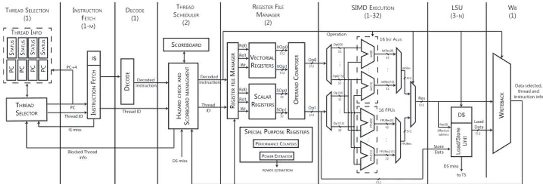
Figure3-1captures a simplified overview of the nu+ many-core. Each nu+
tile has the same basic components, it provides a configurable GPU-like accelerator meant to be used as a configurable FPGA overlay, an extendible coherence subsystem protocol independent, and a mesh-based networking system which routes hardware messages over the communication network.
The accelerator merges the SIMT paradigm with vector processor model. The GPU-like model exposes promising features for improved resource effi-ciency. In fact, it provides hardware threads executing coupled with SIMD execution units, while reducing control overheads and hiding possibly long latencies. This accelerator effectively exploits multi-threading, SIMD op-erations, and low-overhead control flow constructs, in addition to a range of advanced architecture customization capabilities, in order to enable a high-level utilization of the underlying resources. Furthermore, each tile is equipped with both a Cache Controller and a Directory Controller, these handle data coherence among different cores in different tiles, pro-viding a transparent sharing memory programming model to the software developer.