Procedia Engineering 120 ( 2015 ) 1149 – 1152 Available online at www.sciencedirect.com
1877-7058 © 2015 The Authors. Published by Elsevier Ltd. This is an open access article under the CC BY-NC-ND license (http://creativecommons.org/licenses/by-nc-nd/4.0/).
Peer-review under responsibility of the organizing committee of EUROSENSORS 2015
doi: 10.1016/j.proeng.2015.08.742
ScienceDirect
EUROSENSORS 2015
Niobium and tungsten oxide nanowires for chemical sensor
Angela Bertuna
a*, Elisabetta Comini
a, Dario Zappa
a, Giorgio Sberveglieri
aaSENSOR Laboratory, University of Brescia and CNR-INO, Via D. Valotti 9, 25133 brescia, Italy
Abstract
Thin films of tungsten and niobium (WNb) were the starting point for the growth of metal oxide nanowires. RF Magnetron sputtering was used to deposit a layer of 100 nm on 2 Â 2 mm2 alumina substrates. Prepared samples were thermally oxidized to obtain the growth of nanostructures whose morphology was investigated by a scanning electron microscope (SEM). Structural properties of these nanostructures were investigated by RAMAN spectroscopy. Functional characterization was carried out using a homemade test chamber. Interdigitated contacts and heating elements were deposited by DC Magnetron sputtering, and samples were bonded to TO packages thanks to gold wires. The gas sensing properties of samples were analyzed in a wide range of working temperatures for different target gases in order to verify the best working condition. © 2015 The Authors. Published by Elsevier Ltd.
Peer-review under responsibility of the organizing committee of EUROSENSORS 2015.
Keywords: niobium oxide; tungsten oxide; nanowires; thermal oxidation; chemical sensing
1. Introduction
Nowadays the increasing interest in life quality has led to an ever more accurate monitoring of internal and external environments conditions. This motivation, combined with the development of very small sized electronic systems, has brought research to find extremely sensitive and integrated devices. One-dimensional structures are characterized by a great capacity to recognize several target gases due to the high crystallinity and high surface area/volume ratio [1]. Tungsten oxide is widely studied in literature thanks to its functional properties [2]. In this work nanowires of tungsten and niobium oxide were grown directly on the active transducer to solve the problem of reproducibility, contact stability and to allow a direct integration of nanowires into the devices. Nanowires were grown by thermal oxidation in an evaporator furnace provided with a steel chamber.
2. Experimental
At first, a thin film (100 nm) of WNb was deposited on alumina substrates, whose are ultrasonically cleaned in acetone to remove particles that may contaminate the deposition. The starting target was pure tungsten with 12 niobium inserts. Table 1 shows the percentage of niobium and tungsten in the deposited film.
Table 1. Percentage of Nb and W
* Corresponding author. Tel.: +39 0303715873; fax: +39-030-209-1271.
E-mail address: [email protected]
© 2015 The Authors. Published by Elsevier Ltd. This is an open access article under the CC BY-NC-ND license (http://creativecommons.org/licenses/by-nc-nd/4.0/).
1150 Angela Bertuna et al. / Procedia Engineering 120 ( 2015 ) 1149 – 1152
Weight %
Nb 4 W 96
As prepared samples were put inside the evaporator furnace at a working temperature of 550 °C with an oxygen flow of 50 sccm. The thermal oxidation time was set to 1 hour. A rotary pump and a turbo pump have guaranteed low-pressure conditions during the oxidation (10-1 mbar).
A scanning electron microscope (FE-SEM) LEO 1525 was used to investigate nanostructures morphology. The electron beam was set to 7 keV. Samples were fixed to the stub by a carbon-base glue to avoid charge effects.
In order to validate the presence of niobium oxide samples were undergone to Raman spectroscopy. A Peltier-cooled Synapse CCD, a HORIBA monochromator iHR320, a fiber-coupled confocal optical microscope (HORIBA) and a He-Cd laser (442 nm) composed the system for Raman spectroscopy.
Platinum interdigitated contacts and heater were deposited on the transducer by DC magnetron sputtering and gold wires were used to bond the alumina on TO case to realize the sensor. The as obtained devices sensitivity was measured as resistance variation caused by the exposure to different gaseous species. Functional analysis were carried out in a homemade test chamber in which sensors were exposed to several target gases like ethanol, acetone, hydrogen, carbon monoxide, nitrogen dioxide and ammonia
.
Table 2 shows the working conditions of gas sensing.Table 2. Working conditions of gas sensing
Voltage applied
1 V
Chamber temperature
20 °C
Flow 200
sccm
Working temperature
200-550 °C
Stabilization time
10 hours
Time gas in chamber
25 minutes
Time gas out chamber
65 minutes
H
2concentrations
50, 50, 200, 500 ppm
3. Results
SEM is used to investigate the surface of the samples and to check the presence of the nanostructures. Fig.1 shows the density and the nanostructures morphology.
Fig. 1. SEM pictures of prepared nanostructures at 25K (a) and 150K magnification level (b).
1151
Angela Bertuna et al. / Procedia Engineering 120 ( 2015 ) 1149 – 1152
Fig. 2. RAMAN spectrum of WNb oxide (blue) and WO3 (green)
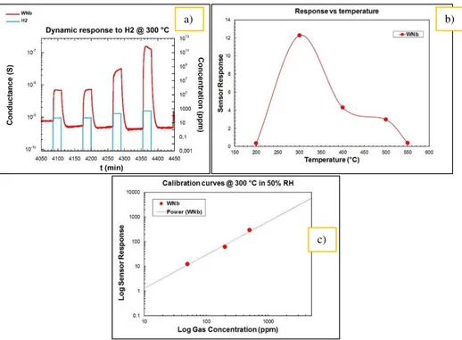
Fig. 2 shows the RAMAN spectrum of as prepared samples in comparison with pure tungsten oxide spectrum. The image underlines a broadening of tungsten oxide peaks in correspondence with the peaks of the oxide of niobium (blue arrows). To verify the ability of the devices to recognize the presence of gaseous species they were exposed to different concentrations of several target gases in a wide range of working temperatures. These sensors give their better responses towards hydrogen in all the range of temperatures and for this reason in this work are shown results towards this gas. Fig. 3 shows, as an example, the dynamic response to hydrogen at 300 °C (a), the sensitivity of the sensor in the range of working temperature (b) and the calibration curve at 300 °C (c).
Fig. 3. Dynamic response of prepared nanostructures to H2 @300 °C RH = 50% (a); response of prepared nanostructures at different temperatures to 50 ppm of H2 (b);
Calibration curve @ 300 °C (c).
a) b)
1152 Angela Bertuna et al. / Procedia Engineering 120 ( 2015 ) 1149 – 1152
The dynamic response underlines the ability of the device to recognize the gas and to recover the baseline in air after the hydrogen exposure. The sensor sensitivity changes in the wide range of working temperatures, as shown in Fig. 3 (b), and it assumes its maximum values at 300 °C showing that the sensor can work better at low temperatures. Calibration curves are in line with the power law.
4. Conclusions
Tungsten and niobium oxide nanostructures on alumina substrates were grown by thermal oxidation technique. As prepared devices were tested as gas sensors to different gaseous species. The dynamic response to hydrogen at 300 °C, which is the optimal working temperature, the sensitivity of the sensor in the range of working temperature to 50 ppm of the same gas and the calibration curve at 300 °C have been shown and discussed.
In conclusion chemical sensors based on tungsten and niobium oxide nanowires have shown good gas sensing performances towards hydrogen at low working temperature. This aspect is important to guarantee safeness in internal and external environmental.
Acknowledgements
The work has been supported by the Italian MIUR through the FIRB Project RBAP115AYN “Oxides at the nanoscale: multifunctionality and applications. This work was partially supported by the European Community’s 7th Framework Programme, under the grant agreement n° 611887 “MSP: Multi Sensor Platform for Smart Building Management”.
References
[1] D. Zappa, E. Comini, G. Sberveglieri, Thermally oxidized zinc oxide nanowires for use as chemical sensors, Nanotechnology 24 (2013) 1-8.