Alberto Fraccarollo, Lorenzo Canti, Leonardo Marchese, and Maurizio Cossi
Citation: The Journal of Chemical Physics 146, 234703 (2017); doi: 10.1063/1.4985054 View online: http://dx.doi.org/10.1063/1.4985054
View Table of Contents: http://aip.scitation.org/toc/jcp/146/23 Published by the American Institute of Physics
THE JOURNAL OF CHEMICAL PHYSICS 146, 234703 (2017)
First principles study of 2D layered organohalide tin perovskites
Alberto Fraccarollo, Lorenzo Canti, Leonardo Marchese, and Maurizio Cossia)Dipartimento di Scienze e Innovazione Tecnologica (DISIT), Universit`a del Piemonte Orientale, Viale T. Michel 11, I-15121 Alessandria, Italy
(Received 6 April 2017; accepted 24 May 2017; published online 16 June 2017)
This article describes the structure and the electronic properties of a series of layered perovskites of a general formula (A+)
2(SnX4) 2where X = I, Br and A+is an organic cation, either formamidinium,
1-methylimidazolium, or phenylethylammonium. For each system, two conformations are consid-ered, with eclipsed or staggered stacking of the adjacent inorganic layers. Geometry optimizations are performed at the density functional theory level with generalized gradient approximation (GGA) functional and semiempirical correction for dispersion energies; band profiles and bandgaps are com-puted including both spin orbit coupling (SOC) and correlation (GW) effects through an additive scheme. The theoretical procedures are validated by reproducing the experimental data of a well known 3D tin iodide perovskite. The results, combined with the calculations previously reported on PbI4analogues, allow us to discuss the effect of cation, metal, and halide substitution in these systems
and in particular to explore the possibility of changing the electronic bandgap as required by different applications. The balance of SOC and GW effects depends on the chemical nature of the studied perovskites and strongly influences the value of the simulated bandgap. Published by AIP Publishing. [http://dx.doi.org/10.1063/1.4985054]
I. INTRODUCTION
Hybrid organic-inorganic perovskites (HOP) formed by various metal halides and organic cations have been the object of intense investigation in the last few years,1–9 prompted by the excellent results reported for photovoltaic devices based on these materials.10–13The largest energy conversion efficiencies have been measured with methylammonium (MA) lead iodide perovskite (MAPbI3), even increased when it is mixed with
other HOP containing formamidinium cations and lead bro-mide14or coupled with IR panchromatic organic absorbers:15 the best result achieved so far exceeds 22% efficiency.16
As a consequence, the search for ever improved materials of this kind is very active: for instance, several studies reported on the effects of metal17–19and halide20–22substitutions in the prototype MAPbI3, involving mostly Sn and Br, respectively.
On the other hand, despite the extremely rich choice of organic cations, almost all the promising perovskites tested for pho-tovoltaics contain methylammonium or formamidinium ions1 (except for a few examples of mixed perovskites including Cs+ or ethylammonium)23–25due to the severe steric limitations of the 3D structure.
Such limitations can be overpassed by resorting to two-dimensional (2D) perovskites, in which metal tetrahalides (MX2−4 ) form layers of corner-sharing octahedra intercalated by mono- or di-valent organic ions:26–31these systems allow a much wider choice of the organic counterpart, their size not being limited by Goldschmidt’s rule. Besides this larger flexi-bility, layered materials can form homogeneous films easily and fill nanoporous matrices, with enhanced mechanical and electronic stability. To design and possibly develop 2D
a)
E-mail: [email protected]
perovskites for photovoltaic applications, as well as for other uses in optoelectronics and microelectronics,1,32–38it is cru-cial to correlate their electronic structure to the structure and the chemical composition.39–42
Since the beginning of this blast of interest in HOP, the-oretical modeling has strongly supported the synthesis and the characterization of 3D perovskites;43–53on the other hand, 2D HOP received less attention, though some recent stud-ies have applied first principles and semiempirical methods to these systems too.41,53–55 Pedesseau et al. have recently reviewed the theoretical methods suitable for the description of 2D organohalide perovskites,9pointing out the importance of including spin-orbit coupling (SOC) for a realistic evaluation of the electronic properties.
In a recent paper,56we have described with ab initio calcu-lations a number of 2D HOP formed by PbI4layers intercalated
by different cations: for all the systems, two geometrical struc-tures were optimized (corresponding to eclipsed and staggered arrangements of the inorganic layers), and the band profiles and gaps were predicted. Furthermore, the relationship between the geometrical parameters (e.g., the interlayer distance and the octahedra distortion) and the electronic properties was discussed.
In the present work, the analysis is extended to investigate the effects of metal and halide substitution on the structures and properties of this class of HOP. Then we modeled differ-ent 2D perovskites formed by SnI4and SnBr4inorganic layers
and three monovalent organic cations, namely, formamidinium (FA), 1-methylimidazolium (MI), and phenylethylammonium (PEA), chosen to have a different chain length, charge den-sity, and ability to form H-bonds. Substituting lead with tin in electronic devices would be beneficial from environmen-tal and health viewpoints; moreover, as discussed below, the
possible applications of lead-based 2D perovskites in pho-tovoltaics are hampered by the high bandgaps, which are expected to decrease after substitution with tin.9,48,57,58
II. METHODS
The geometry optimizations were performed by CRYSTAL0959,60code at the density functional theory (DFT) level, using the PBESOL-D261 functional and including the dispersion energy contributions through the semiempirical procedure proposed by Grimme with the so-called D2 set of parameters.62Both atomic positions and cell parameters were optimized, in the symmetry groups specified below for the var-ious systems. Dunning’s correlation consistent cc-pVDZ basis set63was used, along with small core Stuttgart-K¨oln effective core potentials for Sn, Br, and I.64,65
Electronic band structures and bandgaps were computed with QUANTUM ESPRESSO code, based on the plane wave expansion of the electronic density, with the Perdew-Burke-Ernzerhof (PBE) functional; electronic bands were computed on a 32 k-point path defined in the primitive Brillouin zone (as shown in thesupplementary material). Several studies have pointed out the importance to include both SOC9,43,55,66 and post-DFT correlation energy in the calculation of perovskite bandgaps.9,48Then our calculations were repeated with scalar relativistic (SR) and full relativistic (FR) potentials (in the following, FR-DFT indicates a calculation including SOC): the energy cutoffs were 70 Ry with SR and 45 Ry with FR potentials, respectively; a cutoff of 280 Ry was also used for charge density expansions in FR-DFT. After computing the band structures either at the SR- or at FR-DFT level, the pro-jected density of states (PDOS) was obtained using the atomic wavefunctions provided by QUANTUM ESPRESSO, to eval-uate the contribution of the various elements in the organic and inorganic layers.
The correlation energy was included at the GW level with the same functional: following the same approach previ-ously adopted for the PbI4perovskites,56the polarizability was
expanded on a basis set with 3 Ry cutoff and 2000 basis vectors. The stability of the computed bandgap with respect to these parameters was checked in a test case, as described below.
Since the available version of QUANTUM ESPRESSO allows for GW calculations on the Γ point and with SR poten-tials only, we propose an additive scheme to include both the SOC and correlation in the computed bandgap (Eg),56
Eg = EgSR−DFT+ f EgFR−DFT−ESR−DFTg g +fEgSR−GW(Γ) − EgSR−DFT(Γ) g , (1) where ESR−DFT
g and EgFR−DFT are the bandgaps obtained with
scalar and full relativistic potentials, respectively, on the com-plete 32 k-point path, while ESR−GWg (Γ) and EgSR−DFT(Γ) are computed with and without GW correlation, respectively, on the Γ point.
A number of methodological issues, including the effect of the density functional and the k-point path, have been already discussed for analogous systems based on lead iodide in Ref.56. In that work, the geometry optimization method and the use of Eq.(1)for the bandgap calculation were validated
by reproducing some experimental and theoretical results on the well known (CH3NH3) PbI3 3D perovskite: here we use
the same approach, checking our method on the 3D tin ana-logue, (CH3NH3) SnI3, for which reliable literature data are
available as well.17,48,67
III. RESULTS AND DISCUSSION A. Structure optimizations
In this paper, a total of six 2D perovskites of a general formula (A+)2SnX−24 were considered (A = FA, MI, PEA; X
= Br, I): each system was optimized in two different arrange-ments, corresponding to either eclipsed or staggered stacking of the metal centers on two successive layers.39
Few 2D HOP based on tin halide have been charac-terized by single crystal X-ray diffraction so far: Knutson et al.68reviewed some SnI
4structures intercalated by PEA34,69
or related cations (with various substitutions on the phenyl ring),70,71 which crystallized in the monoclinic system, with C2/m, C2/c, P21/c space groups; the same inorganic
layers with the bulkier trimethylammonio-ethylammonium (TMAEA) cation yielded orthorhombic crystals in the Cmca group,72 while the long chain n-butylammonium and n-dodecylammonium provided orthorhombic (Pbca)73 and triclinic (P ¯1)74 structures, respectively. Mao et al. recently reported58 two structures of SnI4 intercalated by the
mono-valent benzylammonium and dimono-valent histammonium cations, which crystallize in the orthorhombic system (Pbca group) and in the monoclinic system (P21/n), respectively. In
gen-eral, tin-based HOP are found to be isostructural to their Pb counterparts.
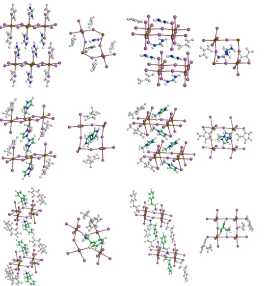
On this basis, as already done for Pb-based HOP,56 eclipsed structures were optimized as monoclinic lattices with the P21/a space group, while for staggered systems, a
tri-clinic lattice was selected, lowering the space symmetry to P1. The latter choice leaves the largest conformational free-dom, allowing us to include all the organic atoms without artificial symmetry constraints. All the optimizations were performed with CRYSTAL09 at the DFT level as described above: the perovskites based on SnI4 are depicted in Fig.1,
while the SnBr4counterparts are illustrated in the
supplemen-tary material, along with the coordinates of all the optimized structures.
The electronic properties of 3D and 2D HOP are strongly related to the geometrical distortions of the inorganic layers, induced by the intercalated cations:9,53this is particularly true for layered systems, as the organic component can vary widely in size, charge density, and ability to form H-bonds, causing correspondingly large deformations of the inorganic layers. While in 3D HOP, it has been observed that the bandgap vari-ations are related mainly to octahedra tilting, the role of this and similar parameters is less understood for 2D systems, where one has to consider the effect of the interlayer distance also on the electronic properties.
The various effects can be quantified by introducing some structural parameters, to describe the inorganic deformation with respect to a “perfect cell,” along with the interlayer distances. Unlike in 3D HOP, in which a really undistorted reference cell can be defined,75choosing a reference structure
234703-3 Fraccarollo et al. J. Chem. Phys. 146, 234703 (2017)
FIG. 1. Optimized structures of A2SnI4perovskites, with A = FA, MI,
PEA, in the eclipsed and staggered arrangement.
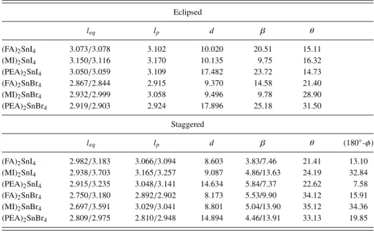
for layered perovskites is less immediate: here we resort to the three angles illustrated in Fig.2to describe the distortion of the inorganic layers.
Angle θ indicates the octahedra tilting, φ indicates the octahedra distortion, and β indicates the displacement of metal
FIG. 2. Structural parameters for HOP: (a) interlayer distance, d; (b) octa-hedron tilting angle, θ; (c) octaocta-hedron deformation angle, φ; (d) metal atom displacement angle, β.
atoms inside the layer (their reference values being 0◦, 180◦, and 0◦, respectively). In addition, equatorial (l
eq) and polar (lp)
metal-halide distances will be tabulated, along with the inter-layer distance d, which corresponds to the distance between the metal planes in two successive layers. These structural param-eters are listed for all the optimized perovskites in TableI: note that the eclipsed structures are subjected to higher symmetry constraints, so that they can exhibit only two values for leqand
one for lp, and φ is fixed to 180◦, while in staggered systems,
these limitations are relaxed.
In both iodide and bromide systems, the interlayer dis-tance d is much smaller with FA and MI cations than with the bulkier PEA; as expected, in the staggered arrangement, d decreases for the greater interpenetration of organic and inorganic layers: this effect is more pronounced with PEA, where π stacking pulls the phenyl rings closer in the stag-gered structures. As noted above, in stagstag-gered structures, all the metal-halide distances can vary independently: in TableI, the two extreme values of leqare reported for staggered HOP.
The longest metal-halide bond distances are induced by the MI cation, with both halides and in both arrangements; the range of variation of leq and (in staggered structures) lp can
be used to estimate the deformation of metal halide octahe-dra: this parameter indicates that staggered systems are more distorted than eclipsed ones, with both halides.
TABLE I. Main structural parameters (Å and degrees) optimized for HOP inorganic layers: equatorial (leq) and
polar (lp) Sn–X bond lenghts, interlayer distance (d), intra-layer metal displacement (β), octahedra tilting (θ), and
deformation (φ) (see also Fig.2). Note that the octahedra deformation is reported as 180◦-φ so that all the angles become 0◦in undistorted structures.
Eclipsed leq lp d β θ (FA)2SnI4 3.073/3.078 3.102 10.020 20.51 15.11 (MI)2SnI4 3.150/3.116 3.170 10.135 9.75 16.32 (PEA)2SnI4 3.050/3.059 3.109 17.482 23.72 14.73 (FA)2SnBr4 2.867/2.844 2.915 9.370 14.58 21.40 (MI)2SnBr4 2.932/2.999 3.058 9.496 9.78 28.90 (PEA)2SnBr4 2.919/2.903 2.924 17.896 25.18 31.50 Staggered leq lp d β θ (180◦-φ) (FA)2SnI4 2.982/3.183 3.066/3.094 8.603 3.83/7.46 21.41 13.10 (MI)2SnI4 2.938/3.703 3.165/3.257 9.087 4.86/13.63 24.19 32.84 (PEA)2SnI4 2.915/3.235 3.048/3.141 14.634 5.84/7.37 22.62 7.58 (FA)2SnBr4 2.750/3.180 2.892/2.902 8.173 5.53/9.90 34.12 15.91 (MI)2SnBr4 2.697/3.591 3.029/3.041 8.801 5.04/13.90 35.12 34.36 (PEA)2SnBr4 2.809/2.975 2.810/2.948 14.894 4.46/13.91 33.13 19.85
On the other hand, the in-plane deformation of the tin atom lattice, measured by angle β, is much more pronounced in the eclipsed arrangement, while the opposite is true for the octahedra tilting, as shown by the larger value of angle θ in staggered structures [here the distortion is also measured by φ, which is especially large for (MI)2SnX4]. It is worth noting
that the MI cation caused the largest distortion also in a series of 2D PbI4HOP with different organic layers,56probably due
to its quite large lateral steric hindrance and incapacity to form H-bonds to the halide atoms.
Among the systems studied here, (PEA)2SnI4, as well
as some derivatives with various phenyl ring substitutions, has been best characterized experimentally:68 Papavassiliou et al.69 proposed a (monoclinic) staggered structure with d = 16.3 Å, and Xu et al.71found increasing values for the interlayer distance of a series of eclipsed meta-substituted (X PEA)2SnI4 (d = 16.7, 16.9, 18.5 Å for X = F, Cl,
Br, respectively). In all these structures the organic layer was found disordered and in the staggered structure described in Ref. 69. The interpenetration of PEA cations is much less pronounced than in our optimized geometry, hence the larger interlayer distances. Apparently the optimized structures (at least for the staggered arrangement) describe minimum energy situations which can be perturbed by thermal motions in the actual samples: the effect of the interlayer distance on
the computed electronic properties will be analyzed in the following.
B. Electronic properties and bandgaps
As anticipated above, the procedure described in Sec.II was validated optimizing the structure and computing the bandgap of 3D (CH3NH3)SnI3. The geometry was optimized
in the tetragonal system, in agreement with the experimen-tal determination,17lowering the space group symmetry from I4/mcm to P ¯4 to allow the unique definition of all the hydro-gen atoms. One can see that the structure is reproduced fairly well, as already found for the lead-based analogue. Then the bandgap was computed at SR-DFT and FR-DFT, and with GW correction, and the best estimate was obtained through Eq.(1): the results are compared to the experimental and to the best available theoretical bandgaps in TableII.
Note that in Ref.48, GW calculations were not limited to the Γ point nor to SR potentials, so that it was possible to compute directly the bandgap including both SOC and corre-lation effects; nonetheless, our additive approach resulted in very good agreement with both this theoretical and the exper-imental results, thus confirming the reliability of Eq.(1)used in the present work.
The band structures of all the 2D perovskites optimized above were computed at SR-DFT and FR-DFT levels, as
TABLE II. Experimental and computed bandgap (eV) for (CH3NH3)SnI3.
This work Reference48
Expt. SR-DFT FR-DFT SR-GW(Γ) Equation(1) SR-DFT FR-DFT SR-GW FR-GW
1.20a 0.64 0.33 1.63 (0.80)b 1.13 0.61 0.31 1.55 1.10
aReference17.
234703-5 Fraccarollo et al. J. Chem. Phys. 146, 234703 (2017)
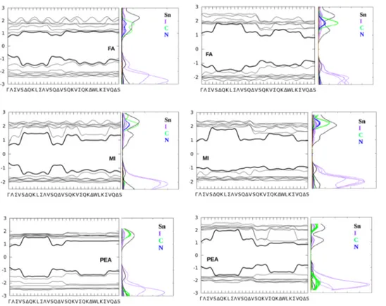
FIG. 3. Electronic energy band profiles and PDOS computed at the SR-DFT level for A2SnI4HOP.
described in Sec.II. The SR-DFT results for SnI4 and SnBr4
HOP are shown in Figs. 3 and 4, respectively, along with the corresponding PDOS to estimate the contribution of the various elements.
All the eclipsed HOP present direct gaps in the Γ point, while indirect gaps are found for staggered systems: an oppo-site behavior was described for the PbI4 analogues with the
same intercalates discussed in Ref.56.
FIG. 4. Electronic energy band profiles and PDOS computed at the SR-DFT level for A2SnBr4HOP.
Some useful insights can be obtained by the analysis of PDOS (another pictorial comparison of all the PDOS is pro-vided in thesupplementary material, Fig. S3, along with some magnified pictures of the region around the gap, Fig. S4 of the supplementary material). For all the systems, the valence band maximum is dominated by the Sn orbital contribution, with the partial exception of eclipsed FA2SnI4where organic (carbon)
atoms contribute as well; the conduction band minimum is always due to a mix of Sn and halide orbitals, in agreement with the findings on other layered58 or 3D76HOP. In these, as in other analogous hybrid perovskites, the contribution of the organic cation to the bandgap seems essentially indirect, related to the geometrical deformations induced in the inor-ganic layer and possibly to H-bonds to halide atoms, rather than to a direct contribution from the molecular orbitals.
SOC effects are expected to reduce substantially the bandgap, as already found for 3D and 2D lead and tin based perovskites: for instance, the importance of SOC for HOP property calculation is pointed out with a variety of exam-ples in Refs. 43 and 53. On the other hand, it is widely assumed that correlation corrections are necessary, in addition to SOC, to obtain reliable bandgap values (the well known case of MAPbI3, for which the SR-DFT bandgap is in
excel-lent agreement with the experiment, due to a fortuitous can-cellation of errors): as explained above, here correlation is included through the GW procedure, as an additive correction to FR-DFT gaps [Eq.(1)].
All the computed bandgaps are listed in TableIII, with the explicit indication of the various contributions: to highlight the effects of metal and halide substitution, the values for A2PbI4
systems computed in Ref. 56with the same approach were also reported.
First, we analyze our best bandgap estimates, including SOC and GW effects (Eg in the last column of TableIII): to
facilitate the comparison, they are also represented in Fig.5. In eclipsed HOP, the substitution of Pb with Sn leads to a systematic reduction of the bandgap, as already observed in the case of 3D perovskites with methylammonium and for-mamidinium: in the present case, this reduction amounts to 13%–15%. On the other hand, substituting tin iodide with tin bromide markedly increases Egfor MI and PEA (around 35%
increase) and to a lesser extent (15%) for FA. The situation is quite different for staggered systems: here, only (PEA)2SnI4
has a lower Eg than its Pb-based counterpart, while with FA
the gap is almost unchanged and with MI it is even increased with respect to the PbI4analogue; also in this case, Eg
broad-ens with bromide, providing the largest bandgaps among all the computed systems (Fig.5).
It was already noted that 2D HOP based on PbI4inorganic
layers are not likely to be useful in photovoltaic applications due to their large bandgaps, which are only loosely depen-dent on the interlayer distance and cannot be reduced below 2 eV even by varying the chemical nature of the intercalated cation. [In Ref. 56, the computed Eg for PbI4 HOP with a
TABLE III. Electronic bandgaps (eV) computed for eclipsed and staggered perovskites with scalar (SR) and full relativistic (FR) pseudopotentials, at the DFT and GW levels.
Eclipsed
ESR
g EgFR SOC correct.a EGWg (Γ) EgSR(Γ) GW correct.b Egc
(FA)2SnI4 1.36 1.20 0.16 2.38 1.36 1.02 2.23 (MI)2SnI4 1.27 1.03 0.24 2.31 1.27 1.04 2.07 (PEA)2SnI4 1.60 1.43 0.17 2.83 1.60 1.23 2.66 (FA)2SnBr4 1.31 1.21 0.10 2.71 1.31 1.39 2.61 (MI)2SnBr4 1.68 1.49 0.19 3.01 1.68 1.33 2.82 (PEA)2SnBr4 2.15 2.05 0.10 3.69 2.15 1.54 3.60 (FA)2PbI4d 2.21 1.48 0.73 3.33 2.21 1.12 2.60 (MI)2PbI4d 2.02 1.26 0.76 3.14 2.01 1.13 2.39 (PEA)2PbI4d 2.37 1.76 0.61 3.86 2.49 1.37 3.13 Staggered
EgSR EgFR SOC correct.a EgGW(Γ) EgSR(Γ) GW correct.b Egc
(FA)2SnI4 1.62 1.35 0.27 3.36 2.23 1.13 2.48 (MI)2SnI4 1.78 1.57 0.21 3.00 1.87 1.13 2.70 (PEA)2SnI4 1.55 1.32 0.23 3.28 1.94 1.34 2.66 (FA)2SnBr4 2.12 1.87 0.25 4.47 2.95 1.52 3.39 (MI)2SnBr4 2.37 2.29 0.08 4.04 2.53 1.51 3.80 (PEA)2SnBr4 2.14 1.94 0.20 4.37 2.91 1.45 3.39 (FA)2PbI4d 2.19 1.36 0.83 3.87 2.74 1.13 2.49 (MI)2PbI4d 2.13 1.39 0.74 3.41 2.19 1.22 2.61 (PEA)2PbI4d 2.30 1.45 0.85 4.57 3.15 1.42 2.87 aDifference between columns 3 and 2: EFR
g −ESRg . bDifference between columns 5 and 6: EGW
g (Γ) − EgSR(Γ). cBest estimate of the bandgap from Eq.(1)or equivalently EFR
g + GW correction. (column 3 + 7). dReference56.
234703-7 Fraccarollo et al. J. Chem. Phys. 146, 234703 (2017)
FIG. 5. Computed bandgaps (eV, last column of TableIII) for eclipsed and staggered A2SnX4, A = FA, MI, PEA, and X = I, Br. The bandgaps for the
same cations in PbI4HOP56are also shown for comparison.
variety of monovalent cations ranges from 2.39 to 3.13 eV for eclipsed and from 2.49 to 2.87 eV for staggered perovskites, with the exception of staggered (EMI)2PbI4, where
ethyl-methylimidazolium induces an unusually large gap of 3.20 eV.] Indeed, one of the reasons to extend the investigation to tin halide 2D perovskites was the hope to obtain substantially lower bandgaps: as shown above, the computed gaps for SnI4
HOP are actually lower than those for PbI4, but the difference
is in general quite small. For comparison, in the already men-tioned 3D MA perovskites, passing from MAPbI3to MASnI3
lowers the bandgap from 1.60 to 1.20 eV (25% reduction). It is interesting to consider the various contributions to Eg
separately: we see that SR-DFT bandgaps are actually much smaller for SnI4 than for PbI4systems, while the presence of
bromide increases them, though the values remain in general below the corresponding PbI4gaps. SOC reduces the value of
bandgaps for all the systems, as expected, but the reduction is markedly smaller in Sn-based than in Pb-based HOP: this is not surprising either due to the smaller atomic number of tin. For the same reason, SOC correction is even smaller in bro-mide than in iodide HOP. On the other hand, GW corrections are similar for all the studied systems, with values approxi-mately in the order SnI4≤PbI4 < SnBr4. As a consequence,
GW positive corrections are less balanced by SOC negative changes in SnI4 than in PbI4, and the differences in final Eg
are smaller than in the initial SR-DFT values, while SnBr4
systems end up with the largest gaps.
A few optical absorption measures performed on SnX4, as
well as PbX4, HOP have shown intense excitonic peaks. This
is related to the unusually strong exciton binding energy due to quantum confinement effects which are much larger in 2D systems than in tridimensional analogues: various authors have estimated such binding energy around 0.2–0.3 eV.72,77–79The exciton energy of (PEA)2SnI4was measured at 2.04 eV;1,68a
number of related compounds where PEA was substituted by halogen atoms in 2- and 4-ring positions showed similar exci-ton energies between 2.02 and 2.23 eV. Absorption energies in the same range were measured for other (RNH3)2SnI4
sys-tems with aliphatic ammonium cations (exciton peaks at 2.04 and 2.14 eV with R = n-butyl73and n-dodecyl,74respectively). Mao et al. reported an optical bandgap of 1.89 eV for SnI4HOP
intercalated by benzylammonium cations (differing from PEA only for a –CH2– group), pointing out the presence of
exci-ton peaks near the absorption edge. Interestingly, these authors also found an even lower absorption edge (1.67 eV) for the sys-tem intercalated by the divalent histammonium cation, as well as for a series of multilayer compounds mixing the character-istics of 3D and 2D HOP (the so-called Ruddlesden-Popper structures).58
The absorption experiments, combined with the estimated exciton binding energy mentioned above, suggest that the elec-tronic bandgap for SnI4HOP is expected around 2.25–2.35 eV
for (PEA)2SnI4, increased up to 2.45–2.55 eV for substituted
PEA, and as low as 2.1–2.2 eV for benzylammonium. Hence the bandgaps reported in Table IIIseem somehow overesti-mated for (PEA)2SnI4, either eclipsed or staggered, while with
the shorter intercalates, Egfalls in the observed range, though
the experiments are not referred to these cations.
These results signal that SOC and GW effects in Eq.(1) could be less effectively balanced for tin-based HOP, leading to slightly overestimated gaps. Pedesseau et al. computed the spin-orbit coupling for a number of 2D HOP based on lead and tin iodide,9 finding that SOC effects reduce the bandgap by 0.70-0.81 eV with Pb and 0.15-0.25 eV with Sn: these variations are in good agreement with our results listed in TableIII.
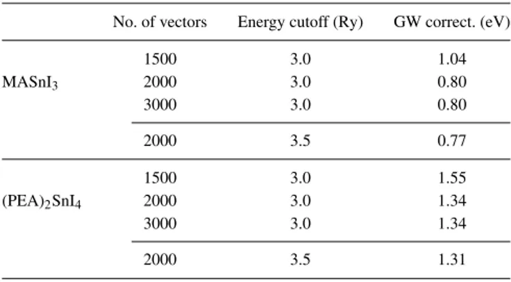
As for GW effects, there are less theoretical estimates to compare with the present calculations: then we decided to test the stability of our results with respect to the parameters used in the polarizability expansion. The bandgaps of 3D MASnI3
and staggered 2D (PEA)2SnI4 were recomputed varying the
number of basis vectors and the energy cutoff, with the results reported in Table IV. In both systems, the GW correction reduces markedly passing from 1500 to 2000 basis vectors, but it is unchanged when the number is further increased to 3000; with 2000 vectors, increasing the cutoff from 3 to 3.5 Ry causes a very small reduction of the GW contribution. Then we conclude that the calculation is stable and reliable with the adopted parameters, i.e., 2000 vectors and 3.0 Ry cutoff.
C. Effect of geometry changes
To compare the computed properties with a few available experimental data, one has to consider also the possible mis-match of the geometrical structures. Even if the crystal system and symmetry group correspond, the position of light atoms
TABLE IV. GW correction (difference between GW and DFT bandgaps at Γ) with a different number of basis vectors and different energy cutoffs.
No. of vectors Energy cutoff (Ry) GW correct. (eV)
MASnI3 1500 3.0 1.04 2000 3.0 0.80 3000 3.0 0.80 2000 3.5 0.77 (PEA)2SnI4 1500 3.0 1.55 2000 3.0 1.34 3000 3.0 1.34 2000 3.5 1.31
is always difficult to specify experimentally: moreover, ther-mal effects are expected to disorder and distort the minimum energy structures.
We tried to evaluate the effect of some distortions with respect to the optimized geometries as follows. First, the inter-layer distance of (PEA)2SnI4, the most studied member of this
family, was modified: in one of the above cited experimental studies,69(PEA)
2SnI4was found in the staggered arrangement
with d = 16.3 Å, while the optimized value reported in TableIis 14.6 Å. Then we increased the interlayer distance to 16.3 Å and reoptimized the position of the organic cations, keeping all the parameters of the inorganic layer frozen as in the minimized structure.
Then the bandgap was recomputed: with the SR potential, the bandgap is 1.65 eV (compared to 1.55 eV for the optimized structure), the SOC correction is 0.22 eV ( 0.23), and the GW correction is 1.79 eV (1.34). Applying Eq.(1),we obtain the best estimate of Eg, 3.22 eV (compared to 2.66 eV with d
= 14.6 Å): the difference is partly due to the SR gap but mostly due to the markedly higher GW correction. For comparison, a similar increment of the interlayer distance of (PEA)2PbI4
(in that case d was increased from 15.2 to 16.7 Å) caused a much smaller growth of the computed bandgap, from 3.13 to 3.22 eV.56
The same test was performed on staggered (FA)2SnI4,
increasing the interlayer distance to 9.6 Å, around 11% larger than the previously optimized value, and reoptimizing the other parameters. The SR bandgap is 1.65 eV (1.62 in the fully opti-mized structure), the SOC correction is 0.27 eV ( 0.27), and the GW correction is 1.20 eV (1.13): as a result, the best esti-mate of Egis 2.58 eV, compared to 2.48 eV in the optimized
structure. In Ref.56, the bandgap of eclipsed (FA)2PbI4was
found to increase from 2.60 to 3.21 eV after a similar interlayer distance increase.
Apparently, then, (PEA)2SnI4 is more sensitive to the
interlayer distance than its lead-base counterparts, while the opposite is true for the systems with the FA cation.
The effect of H-bonds between the organic cation and the halogen atoms in the inorganic layer was also evaluated for PEA cations: this interaction is considered important to deter-mine the value of HOP electronic properties,1 and it is also
FIG. 6. Computed bandgaps [eV, from Eq.(1)] for staggered (PEA)2SnI4as
a function of –NH3rotating angle: 0 corresponds to the optimized structure,
with the strongest H-bond.
likely perturbed by thermal effects. Starting from the opti-mized structure of staggered (PEA)2SnI4, we recomputed the
bandgap after rotating the –NH3group, with the results shown
in Fig.6: this geometrical parameter appears much less impor-tant for the bandgap value, which varies only by 0.045 eV during the rotation.
In general, thermal disorder and distortions are expected to increase the computed bandgap, with an effect much more pronounced for the interlayer distance.
IV. CONCLUSIONS
The structure and the electronic properties of a series of layered perovskites based on tin halide sheets intercalated by organic cations were modeled with state-of-the-art quantum mechanical methods.
The optimized structures, both in eclipsed and in stag-gered conformations, show different degrees of distortion of the inorganic layers: some features are similar to those pre-viously found for the lead iodide analogues, but a clear trend relating the nature of the intercalate with the layer deforma-tion does not emerge easily. Moreover, a few experimental data available indicate that thermal disorder is likely to move the systems away from the equilibrium structures, especially in the organic interlayer.
The band profiles (both at the SR- and FR-DFT level) show that the bandgaps are direct for eclipsed and indirect for staggered arrangements, with both halides. From the PDOS analysis, we conclude that in the systems studied here, the role of the cations on the bandgap is essentially indirect, due to the geometric distortions induced on the inorganic sheets, and not involving the organic orbitals directly.
Bandgap values, as well as their dependence on chem-ical and structural variations, are of paramount importance in photovoltaic and optoelectronic applications. The proce-dure adopted here, validated by reproducing the bandgap of well known 3D HOP based on lead and tin iodide, provides reliable electronic properties, including both SOC and GW correlation effects through an additive scheme. Combining the present results with the calculations previously reported on various PbI4layered HOP, we have discussed the effect of
cation, metal, and halide substitutions. For instance, varying the cations in MX4homologue series can modify the bandgap
30%-40% in eclipsed and 10%-20% in staggered conforma-tions, and substituting tin for lead reduces the gap about 15% in eclipsed systems, while leaving it unchanged or even increased in staggered structures. The discrepancy of this behavior with that observed in 3D HOP has been discussed in terms of the balance of SOC and GW corrections.
Such knowledge can be of help in designing new HOP tai-lored for specific applications, even if the rich choice of organic cations suitable for intercalation in these layered systems calls for further work to extend the present analysis.
SUPPLEMENTARY MATERIAL
See supplementary material for an illustration of the 32 k-point path along which the electronic bands are com-puted, some pictures of the optimized SnBr4 systems, and a
234703-9 Fraccarollo et al. J. Chem. Phys. 146, 234703 (2017)
comparison of PDOS. The coordinates of all the optimized perovskites are provided as well.
ACKNOWLEDGMENTS
This work was funded by EU in the framework of the HORIZON2020 program, through the project MULTI2HYCAT (NMBP-01-2016-720783), and by the Ital-ian Ministry of Education, University and Research (PRIN-2010A2FSS9).
1B. Saparov and D. B. Mitzi, “Organic-inorganic perovskites: Structural
ver-satility for functional materials design,”Chem. Rev.116(7), 4558–4596 (2016).
2L. Etgar, P. Gao, Z. Xue, Q. Peng, A. K. Chandiran, B. Liu, Md. K.
Nazeerud-din, and M. Gr¨atzel, “Mesoscopic CH3NH3PbI3/TiO2heterojunction solar
cells,”J. Am. Chem. Soc.134, 17396–17399 (2012).
3J. H. Heo, S. H. Im, J. H. Noh, T. N. Mandal, C.-S. Lim, J. A. Chang, Y.
H. Lee, H.-J. Kim, A. Sarkar, M. K. Nazeeruddin, M. Gr¨atzel, and S. I. Seok, “Efficient inorganic-organic hybrid heterojunction solar cells containing perovskite compound and polymeric hole conductors,”Nat. Photonics7(6), 486–491 (2013).
4N.-G. Park, “Organometal perovskite light absorbers toward a 20%
effi-ciency low-cost solid-state mesoscopic solar cell,”J. Phys. Chem. Lett.4, 2423–2429 (2013).
5H. J. Snaith, “Perovskites: The emergence of a new era for low-cost,
high-efficiency solar cells,”J. Phys. Chem. Lett.4, 3623–3630 (2013).
6M. A. Green, A. Ho-Baillie, and H. J. Snaith, “The emergence of perovskite
solar cells,”Nat. Photonics8(7), 506–514 (2014).
7S. Luo and W. A. Daoud, “Recent progress in organic-inorganic halide
perovskite solar cells: Mechanisms and material design,”J. Mater. Chem. A3(17), 8992–9010 (2015).
8S. Collavini, S. F. V¨olker, and J. L. Delgado, “Understanding the
outstand-ing power conversion efficiency of perovskite-based solar cells,”Angew. Chem., Int. Ed.54(34), 9757–9759 (2015).
9L. Pedesseau, D. Sapori, B. Traore, R. Robles, H.-H. Fang, M. A. Loi,
H. Tsai, W. Nie, J.-C. Blancon, A. Neukirch, S. Tretiak, A. D. Mohite, C. Katan, J. Even, and M. Kepenekian, “Advances and promises of layered halide hybrid perovskite semiconductors,”ACS Nano10(11), 9776–9786 (2016).
10H. Zhou, Q. Chen, G. Li, S. Luo, T.-B. Song, H.-S. Duan, Z. Hong, J. You,
Y. Liu, and Y. Yang, “Interface engineering of highly efficient perovskite solar cells,”Science345(6196), 542–546 (2014).
11H.-S. Kim, C.-R. Lee, J.-H. Im, K.-B. Lee, T. Moehl, A. Marchioro,
S.-J. Moon, R. Humphry-Baker, J.-H. Yum, J. E. Moser, M. Gr¨atzel, and N.-G. Park, “Lead iodide perovskite sensitized all-solid-state submicron thin film mesoscopic solar cell with efficiency exceeding 9%,”Sci. Rep.2, 591 (2012).
12D. Bi, W. Tress, M. I. Dar, P. Gao, J. Luo, C. Renevier, K. Schenk, A. Abate,
F. Giordano, J.-P. Correa Baena, J.-D. Decoppet, S. M. Zakeeruddin, M. K. Nazeeruddin, M. Gr¨atzel, and A. Hagfeldt, “Efficient luminescent solar cells based on tailored mixed-cation perovskites,”Sci. Adv.2(1), e1501170 (2016).
13M. Saliba, T. Matsui, J.-Y. Seo, K. Domanski, J.-P. Correa-Baena, M.
K. Nazeeruddin, S. M. Zakeeruddin, W. Tress, A. Abate, A. Hagfeldt, and M. Gr¨atzel, “Cesium-containing triple cation perovskite solar cells: Improved stability, reproducibility and high efficiency,”Energy Environ. Sci.9(6), 1989–1997 (2016).
14J. Seo, J. H. Noh, and S. I. Seok, “Rational strategies for efficient perovskite
solar cells,”Acc. Chem. Res.49(3), 562–572 (2016).
15T. Kinoshita, K. Nonomura, N. J. Jeon, F. Giordano, A. Abate, S. Uchida,
T. Kubo, S. I. Seok, M. K. Nazeeruddin, A. Hagfeldt, M. Gr¨atzel, and H. Segawa, “Spectral splitting photovoltaics using perovskite and wideband dye-sensitized solar cells,”Nat. Commun.6, 8834 (2015).
16 Seehttp://www.nrel.gov/pv/assets/images/efficiency-chart.pngfor
infor-mation about the record efficiencies of photovoltaic systems (January 2017).
17C. C. Stoumpos, C. D. Malliakas, and M. G. Kanatzidis, “Semiconducting
tin and lead iodide perovskites with organic cations: Phase transitions, high mobilities, and near-infrared photoluminescent properties,”Inorg. Chem.
52, 9019–9038 (2013).
18N. K. Noel, S. D. Stranks, A. Abate, C. Wehrenfennig, S. Guarnera, A.-A.
Haghighirad, A. Sadhanala, G. E. Eperon, S. K. Pathak, M. B. Johnston,
A. Petrozza, L. M. Herz, and H. J. Snaith, “Lead-free organic-inorganic tin halide perovskites for photovoltaic applications,”Energy Environ. Sci.
7(9), 3061–3068 (2014).
19F. Hao, C. C. Stoumpos, D. H. Cao, R. P. H. Chang, and M. G. Kanatzidis,
“Lead-free solid-state organic-inorganic halide perovskite solar cells,”Nat. Photonics8(6), 489–494 (2014).
20M. M. Lee, J. Teuscher, T. Miyasaka, T. N. Murakami, and H. J. Snaith,
“Efficient hybrid solar cells based on meso-superstructured organometal halide perovskites,”Science338(6107), 643–647 (2012).
21M. Liu, M. B. Johnston, and H. J. Snaith, “Efficient planar heterojunction
perovskite solar cells by vapour deposition,”Nature501(7467), 395–398 (2013).
22J. H. Noh, S. H. Im, J. H. Heo, T. N. Mandal, and S. I. Seok, “Chemical
management for colorful, efficient, and stable inorganic-organic hybrid nanostructured solar cells,”Nano Lett.13(4), 1764–1769 (2013).
23C. Yi, J. Luo, S. Meloni, A. Boziki, N. Ashari-Astani, C. Gr¨atzel, S.
M. Zakeeruddin, U. R¨othlisberger, and M. Gr¨atzel, “Entropic stabilization of mixed a-cation ABX3 metal halide perovskites for high performance
perovskite solar cells,”Energy Environ. Sci.9(2), 656–662 (2016).
24J.-H. Im, J. Chung, S.-J. Kim, and N.-G. Park, “Synthesis, structure, and
pho-tovoltaic property of a nanocrystalline 2H perovskite-type novel sensitizer (CH3CH2NH3)PbI3,”Nanoscale Res. Lett.7, 353 (2012).
25W. Peng, X. Miao, V. Adinolfi, E. Alarousu, O. El Tall, A.-H. Emwas,
C. Zhao, G. Walters, J. Liu, O. Ouellette, J. Pan, B. Murali, E. H. Sargent, O. F. Mohammed, and O. M. Bakr, “Engineering of CH3NH3PbI3perovskite
crystals by alloying large organic cations for enhanced thermal stability and transport properties,”Angew. Chem., Int. Ed.55(36), 10686–10690 (2016).
26D. B. Mitzi, “Synthesis, structure, and properties of organic-inorganic
per-ovskites and related materials,” in Progress in Inorganic Chemistry, edited by K. D. Karlin (John Wiley & Sons, Inc., 2007), pp. 1–121.
27D. G. Billing and A. Lemmerer, “Synthesis, characterization and phase
transitions in the inorganic-organic layered perovskite-type hybrids [(CnH2n+1NH3)2PbI4], n= 4, 5 and 6,”Acta Crystallogr., Sect. B: Struct.
Sci.63(5), 735–747 (2007).
28D. G. Billing and A. Lemmerer, “Inorganic-organic hybrid materials
incorporating primary cyclic ammonium cations: The lead iodide series,”
CrystEngComm9(3), 236–244 (2007).
29K. Pradeesh, J. J. Baumberg, and G. V. Prakash, “In situ intercalation
strate-gies for device-quality hybrid inorganic-organic self-assembled quantum wells,”Appl. Phys. Lett.95(3), 033309 (2009).
30A. Lemmerer and D. G. Billing, “Effect of heteroatoms in the
inorganic-organic layered perovskite-type hybrids [(ZCnH2nNH3)2PbI4], n = 2, 3, 4, 5,
6; Z = OH, Br and I; and [(H3NC2H4S2C2H4NH3)PbI4],”CrystEngComm
12(4), 1290–1301 (2010).
31A. Lemmerer and D. G. Billing, “Synthesis, characterization and phase
transitions of the inorganic-organic layered perovskite-type hybrids [(CnH2n+1NH3)2PbI4], n = 7, 8, 9 and 10,”Dalton Trans.41(4), 1146–1157
(2012).
32T. Ishihara, J. Takahashi, and T. Goto, “Optical properties due to electronic
transitions in two-dimensional semiconductors (CnH2n+1NH3)2PbI4,”
Phys. Rev. B42(17), 11099–11107 (1990).
33Q. Chen, N. De Marco, Y. Yang, T.-B. Song, C.-C. Chen, H. Zhao, Z. Hong,
H. Zhou, and Y. Yang, “Under the spotlight: The organic-inorganic hybrid halide perovskite for optoelectronic applications,”Nano Today10(3), 355– 396 (2015).
34C. R. Kagan, D. B. Mitzi, and C. D. Dimitrakopoulos, “Organic-inorganic
hybrid materials as semiconducting channels in thin-film field-effect transistors,”Science286(5441), 945–947 (1999).
35Z.-K. Tan, R. S. Moghaddam, M. L. Lai, P. Docampo, R. Higler, F. Deschler,
M. Price, A. Sadhanala, L. M. Pazos, D. Credgington, F. Hanusch, T. Bein, H. J. Snaith, and R. H. Friend, “Bright light-emitting diodes based on organometal halide perovskite,”Nat. Nanotechnol.9(9), 687–692 (2014).
36X. Wu, M. T. Trinh, D. Niesner, H. Zhu, Z. Norman, J. S. Owen, O. Yaffe,
B. J. Kudisch, and X.-Y. Zhu, “Trap states in lead iodide perovskites,”J. Am. Chem. Soc.137(5), 2089–2096 (2015).
37L. Dou, A. B. Wong, Y. Yu, M. Lai, N. Kornienko, S. W. Eaton, A. Fu, C.
G. Bischak, J. Ma, T. Ding, N. S. Ginsberg, L.-W. Wang, A. P. Alivisatos, and P. Yang, “Atomically thin two-dimensional organic-inorganic hybrid perovskites,”Science349(6255), 1518–1521 (2015).
38F. Deschler, M. Price, S. Pathak, L. E. Klintberg, D.-D. Jarausch, R. Higler,
S. Httner, T. Leijtens, S. D. Stranks, H. J. Snaith, M. Atatre, R. T. Phillips, and R. H. Friend, “High photoluminescence efficiency and optically pumped lasing in solution-processed mixed halide perovskite semiconductors,”J. Phys. Chem. Lett.5(8), 1421–1426 (2014).
39D. B. Mitzi, “A layered solution crystal growth technique and the crystal
structure of (C6H5C2H4NH3)2PbCl4,”J. Solid State Chem.145(2), 694–
704 (1999).
40K. Gauthron, J.-S. Lauret, L. Doyennette, G. Lanty, A. Al Choueiry, S.
J. Zhang, A. Brehier, L. Largeau, O. Mauguin, J. Bloch, and E. Deleporte, “Optical spectroscopy of two-dimensional layered (C6H5C2H4NH3)2PbI4
perovskite,”Opt. Express18(6), 5912–5919 (2010).
41S. Sourisseau, N. Louvain, W. Bi, N. Mercier, D. Rondeau, F. Boucher,
J.-Y. Buzar´e, and C. Legein, “Reduced band gap hybrid perovskites resulting from combined hydrogen and halogen bonding at the organic-inorganic interface,”Chem. Mater.19(3), 600–607 (2007).
42D. H. Cao, C. C. Stoumpos, O. K. Farha, J. T. Hupp, and M. G. Kanatzidis,
“2D homologous perovskites as light-absorbing materials for solar cell applications,”J. Am. Chem. Soc.137(24), 7843–7850 (2015).
43J. Even, L. Pedesseau, J.-M. Jancu, and C. Katan, “Importance of spin–
orbit coupling in hybrid organic/inorganic perovskites for photovoltaic applications,”J. Phys. Chem. Lett.4, 2999–3005 (2013).
44E. Mosconi, A. Amat, Md. K. Nazeeruddin, M. Gr¨atzel, and F. De Angelis,
“First-principles modeling of mixed halide organometal perovskites for photovoltaic applications,”J. Phys. Chem. C117, 13902–13913 (2013).
45F. Brivio, A. B. Walker, and A. Walsh, “Structural and electronic properties
of hybrid perovskites for high-efficiency thin-film photovoltaics from first-principles,”APL Mater.1(4), 042111 (2013).
46W.-J. Yin, T. Shi, and Y. Yan, “Unique properties of halide perovskites as
possible origins of the superior solar cell performance,”Adv. Mater.26(27), 4653–4658 (2014).
47J. Kim, S.-H. Lee, J. H. Lee, and K.-H. Hong, “The role of intrinsic defects
in methylammonium lead iodide perovskite,”J. Phys. Chem. Lett.5(8), 1312–1317 (2014).
48P. Umari, E. Mosconi, and F. De Angelis, “Relativistic GW calculations on
CH3NH3PbI3and CH3NH3SnI3Perovskites for solar cell applications,”
Sci. Rep.4, 4467 (2014).
49E. Mosconi, E. Ronca, and F. De Angelis, “First-principles
investiga-tion of the TiO2/organohalide perovskites interface: The role of interfacial
chlorine,”J. Phys. Chem. Lett.5(15), 2619–2625 (2014).
50A. Torres and L. G. C. Rego, “Surface effects and adsorption of methoxy
anchors on hybrid lead iodide perovskites: Insights for spiro-MeOTAD attachment,”J. Phys. Chem. C118(46), 26947–26954 (2014).
51E. Mosconi, P. Umari, and F. De Angelis, “Electronic and optical properties
of mixed Sn–Pb organohalide perovskites: A first principles investigation,”
J. Mater. Chem. A3(17), 9208–9215 (2015).
52L. Zhang and P. H.-L. Sit, “Ab initio study of interaction of water, hydroxyl
radicals, and hydroxide ions with CH3NH3PbI3and CH3NH3PbBr3
sur-faces,”J. Phys. Chem. C119(39), 22370–22378 (2015).
53J. Even, L. Pedesseau, C. Katan, M. Kepenekian, J.-S. Lauret, D. Sapori,
and E. Deleporte, “Solid-state physics perspective on hybrid perovskite semiconductors,”J. Phys. Chem. C119(19), 10161–10177 (2015).
54T. Umebayashi, K. Asai, T. Kondo, and A. Nakao, “Electronic structures
of lead iodide based low-dimensional crystals,” Phys. Rev. B 67(15), 155405-1–155405-6 (2003).
55J. Even, L. Pedesseau, M.-A. Dupertuis, J.-M. Jancu, and C. Katan,
“Elec-tronic model for self-assembled hybrid organic/perovskite Semiconductors: Reverse band edge electronic states ordering and spin-orbit coupling,”Phys. Rev. B86(20), 205301 (2012).
56A. Fraccarollo, V. Cantatore, G. Boschetto, L. Marchese, and M. Cossi,
“Ab initio modeling of 2D layered organohalide lead perovskites,”J. Chem. Phys.144(16), 164701 (2016).
57T. D. Huan, V. N. Tuoc, and N. V. Minh, “Layered structures of
organic/inorganic hybrid halide perovskites,”Phys. Rev. B93(9), 094105 (2016).
58L. Mao, H. Tsai, W. Nie, L. Ma, J. Im, C. C. Stoumpos, C. D. Malliakas,
F. Hao, M. R. Wasielewski, A. D. Mohite, and M. G. Kanatzidis, “Role of organic counterion in lead- and tin-based two-dimensional semiconduct-ing iodide perovskites and application in planar solar cells,”Chem. Mater.
28(21), 7781–7792 (2016).
59R. Dovesi, R. Orlando, B. Civalleri, C. Roetti, V. R. Saunders, and C.
M. Zicovich-Wilson, “CRYSTAL: A computational tool for the ab initio study of the electronic properties of crystals,” Z. Kristallogr.220(5-6), 571–573 (2005).
60R. Dovesi, V. R. Saunders, C. Roetti, R. Orlando, C. M. Zicovich-Wilson,
F. Pascale, K. Doll, N. M. Harrison, B. Civalleri, I. J. Bush, Ph. D’Arco, and M. Llunell, CRYSTAL09 User’s Manual (Universit`a di Torino, Torino, 2010).
61J. P. Perdew, A. Ruzsinszky, G. I. Csonka, O. A. Vydrov, G. E. Scuseria,
L. A. Constantin, X. Zhou, and K. Burke, “Restoring the density-gradient expansion for exchange in solids and surfaces,”Phys. Rev. Lett.100, 136406 (2008).
62S. Grimme, “Semiempirical GGA-type density functional constructed with
a long-range dispersion correction,”J. Comput. Chem.27(15), 1787–1799 (2006).
63T. H. Dunning, “Gaussian basis sets for use in correlated molecular
calcula-tions. I. The atoms boron through neon and hydrogen,”J. Chem. Phys.90, 1007–1023 (1989).
64K. A. Peterson, B. C. Shepler, D. Figgen, and H. Stoll, “On the spectroscopic
and thermochemical properties of ClO, BrO, IO, and their anions,”J. Phys. Chem. A110(51), 13877–13883 (2006).
65B. Metz, H. Stoll, and M. Dolg, “Small-core
multiconfiguration-Dirac-Hartree-Fock-adjusted pseudopotentials for post-d main group elements: Application to PbH and PbO,”J. Chem. Phys.113(7), 2563–2569 (2000).
66L. Pedesseau, J.-M. Jancu, A. Rolland, E. Deleporte, C. Katan, and J. Even,
“Electronic properties of 2D and 3D hybrid organic/inorganic perovskites for optoelectronic and photovoltaic applications,”Opt. Quantum. Electron.
46(10), 1225–1232 (2014).
67F. Chiarella, A. Zappettini, F. Licci, I. Borriello, G. Cantele, D. Ninno,
A. Cassinese, and R. Vaglio, “Combined experimental and theoretical inves-tigation of optical, structural, and electronic properties of CH3NH3SnX3
thin films (X = Cl, Br),”Phys. Rev. B77(4), 045129 (2008).
68J. L. Knutson, J. D. Martin, and D. B. Mitzi, “Tuning the band gap in hybrid
tin iodide perovskite semiconductors using structural templating,”Inorg. Chem.44(13), 4699–4705 (2005).
69G. C. Papavassiliou, I. B. Koutselas, A. Terzis, and M.-H. Whangbo,
“Structural and electronic properties of the natural quantum-well system (C6H5CH2CH2NH3)2SnI4,”Solid State Commun.91(9), 695–698 (1994). 70D. B. Mitzi, C. D. Dimitrakopoulos, and L. L. Kosbar, “Structurally tailored
organic-inorganic perovskites: Optical properties and solution-processed channel materials for thin-film transistors,”Chem. Mater.13(10), 3728– 3740 (2001).
71Z. Xu, D. B. Mitzi, C. D. Dimitrakopoulos, and K. R. Maxcy,
“Semiconduct-ing perovskites (2-XC6H4C2H4NH3)2Snl4(X = F, Cl, Br): Steric interaction
between the organic and inorganic layers,”Inorg. Chem.42(6), 2031–2039 (2003).
72Z. Xu, D. B. Mitzi, and D. R. Medeiros, “[(CH
3)3NCH2CH2NH3]SnI4:
A layered perovskite with quaternary/primary ammonium dications and short interlayer iodine-iodine contacts,”Inorg. Chem.42(5), 1400–1402 (2003).
73D. B. Mitzi, “Synthesis, crystal structure, and optical and thermal properties
of (C4H9NH3)2MI4(M = Ge, Sn, Pb),”Chem. Mater.8(3), 791–800 (1996). 74Z. Xu and D. B. Mitzi, “[CH
3(CH2)11NH3]SnI3: A hybrid semiconductor
with MoO3-type tin(II) iodide layers,”Inorg. Chem.42(21), 6589–6591
(2003).
75M. R. Filip, G. E. Eperon, H. J. Snaith, and F. Giustino, “Steric engineering
of metal-halide perovskites with tunable optical band gaps,”Nat. Commun.
5, 5757 (2014).
76S. Andalibi, A. Rostami, G. Darvish, and M. K. Moravvej-Farshi, “Band gap
engineering of organo metal lead halide perovskite photovoltaic absorber,”
Opt. Quantum Electron.48(4), 258 (2016).
77S. Ahmad, P. K. Kanaujia, H. J. Beeson, A. Abate, F. Deschler, D.
Credg-ington, U. Steiner, G. V. Prakash, and J. J. Baumberg, “Strong photocurrent from two-dimensional excitons in solution-processed stacked perovskite semiconductor sheets,”ACS Appl. Mater. Interfaces7(45), 25227–25236 (2015).
78V. D’Innocenzo, G. Grancini, M. J. P. Alcocer, A. R. S. Kandada, S.
D. Stranks, M. M. Lee, G. Lanzani, H. J. Snaith, and A. Petrozza, “Excitons versus free charges in organo-lead tri-halide perovskites,”Nat. Commun.
5, 3586 (2014).
79Y. Takahashi, R. Obara, K. Nakagawa, M. Nakano, J.-Y. Tokita, and
T. Inabe, “Tunable charge transport in soluble organic-inorganic hybrid semiconductors,”Chem. Mater.19(25), 6312–6316 (2007).
![FIG. 6. Computed bandgaps [eV, from Eq. (1) ] for staggered (PEA) 2 SnI 4 as](https://thumb-eu.123doks.com/thumbv2/123dokorg/4923615.51410/9.891.85.411.829.1073/fig-computed-bandgaps-ev-eq-staggered-pea-sni.webp)
