1 DOI: 10.1002/adma.((please add manuscript number)) Article type: Communication
A Highly Selective and Self-Powered Gas Sensor via Organic Surface Functionalization of p-Si/n-ZnO Diodes
Martin W. G. Hoffmann, Leonhard Mayrhofer, Olga Casals, Lorenzo Caccamo, Francisco Hernandez-Ramirez, Gerhard Lilienkamp, Winfried Daum, Michael Moseler, Andreas Waag, Hao Shen* and J. Daniel Prades*
M. W. G. Hoffmann, L. Caccamo, Prof. A. Waag, Dr. H. Shen Institute of Semiconductor Technology
Technische Universität Braunschweig, 38106 Braunschweig (Germany) E-mail: [email protected]
M. W. G. Hoffmann, Dr. O. Casals, Dr. F. Hernandez-Ramirez, Dr. J. D. Prades Department of Electronics
University of Barcelona, 08028 Barcelona (Spain) E-mail: [email protected]
Dr. G. Lilienkamp, Prof. W. Daum
Institute of Energy Research and Physical Technologies Technical University Clausthal, 38678 Clausthal (Germany) Dr. L. Mayrhofer, Prof. M. Moseler
Fraunhofer Institute for Mechanics of Materials (IWM) 79108 Freiburg (Germany)
Dr. F. Hernandez-Ramirez
Department of Advanced Materials for Energy Applications Catalonia Institute for Energy Research (IREC)
08930 Barcelona (Spain)
M. W. G. Hoffmann, L. Caccamo, Prof. A. Waag, Dr. H. Shen Laboratory for Emerging Nanometrology
Technische Universität Braunschweig, 38106 Braunschweig (Germany)
Keywords: selective sensing, self-powered, DFT, self assembled monolayers, hybrid materials
Low power consumption and reliable selectivity are the two main requirements for gas sensors to be applicable in mobile devices.[1] These technological platforms, e.g. smart phones or wireless sensor
platforms will facilitate personalized detection of environmental and health conditions, and hence becoming the basis of the future core technology of ubiquitous sensing. Even today, health control as well as environmental monitoring is relying on immobile and complex detection systems with very limited availability in space and time. Recent works have shown promising concepts to realize self-powered gas sensors that are capable of detecting gases without the need of external power sources to
2
activate the sensor-gas interaction or to actively generate a read out signal.[2,3] These sensors
drastically reduce power consumption compared to conventional semiconductor gas sensors and additionally reduce the required space for integration. All these attempts so far were based on purely nano structured inorganic metal oxide sensor materials that provide a good sensitivity towards different gases due to their high surface-to-volume ratio. However, due to their non-selective sensing mechanism based on oxygen vacancy-gas interactions, these purely inorganic sensors cannot
accomplish a meaningful gas selectivity.[4,5]High selectivities towards single gas species have been
recently reported via modifying the inorganic surface of nanostructured semiconductors with a defined organic functionality.[6–9] Theoretical simulations based on ab-initio density functional theory (DFT)
for a system composed of SnO2 NWs modified with a defined self assembled monolayer (SAM)
elucidated the reason for the high selectivity of such gas sensor: the energetic position of the SAM-gas frontier orbitals with respect to the NW Fermi level have been identified to be the crucial factor to ensure an efficient charge transfer upon gas-SAM binding interactions and thus to sense or
discriminate a certain gas species.[7] The high flexibility of organic surface modifications in terms of
functional groups as well as their sterical and electronic structure possibly might enable the targeted design of various specific gas sensors. However, all organic surface modified sensor systems so far are based on compact conductometric or field effect transistor (FET) sensor concepts that still require a remarkable amount of energy to generate a sensor signal (e.g. by applying a source-drain current). Up to date, none of the semiconductor based gas sensor systems could accomplish both, the
self-powered/low powered sensor operation and highly selective gas detection within a single and compact device.
In this work, we present a semiconductor based gas sensor concept that combines the two substantial requirements of mobile gas sensing in a singular sensor device: self-powered operation combined with high gas selectivity. Beyond the combination of self-powered sensing and high selectivity, also a very high sensitivity could also been demonstrated for the exemplified target gas nitrogen dioxide (NO2).
The sensor reported here was capable of detecting NO2 concentrations in the sub ppm level with a very
high selectivity which is a crucial detection region since NO2 is considered to be one of the major
threads for human health and already toxic at very low concentrations (ppb level).[10] NO
3
in urban and industrial environments by various combustion processes and can produce ozone,
respiratory ailments[11] and is suspected to cause cancer.[12] For all these, the here presented technology
could depict an approach for the much sought-after wide spread sensor networks to monitor densely populated areas to improve the ambient air quality.
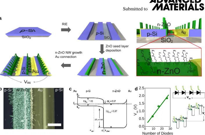
Figure 1a schematically shows the production process of our self-powered and selective sensor device
based on nanostructured p-Si/n-ZnO diodes. After patterning of a p-Si layer on SiO2 via reactive ion
etching (RIE), photolithographic methods were used to deposit layers of 20 nm ZnO selectively on the p-Si sidewalls that served as a seed layer for site selective growth of n-ZnO nanowires to form p-Si/n-ZnO heterojunctions (Figure 1b and c ). X-ray diffraction spectra revealed a good crystallinity and a disproportionate peak attributed to the ZnO (002) facet indicated an oriented growth direction along the c-axis (Figure S1). Under illumination with solar light (AM1.5), an open circuit voltage (Voc) is
induced by the build-in potential at the p-n heterojunction[2,13,14] that is used as a self-generated signal
for the sensor. To ensure a strong and measurable Voc signal even under low illumination conditions,
every device contained several diodes connected in series by evaporated gold contacts (9, 16 or 26 diodes; see Figure 1c). This configuration resulted in a linear increase of the measured Voc signal
proportional with the number of diodes in series under light, with an average contribution of Voc,exp =
72 ± 6 mV/diode (typical value for p-Si/n-ZnO diodes)[2] and leads to measured values of 0.65 V (9
diodes), 1.35 V (16 diodes) and 1.84 V (26 diodes) respectively (see Figure 1c andFigureS2 in supporting information).
Figure 1d shows the band diagram of the Au/p-Si/n-ZnO/Au system in equilibrium (see supporting information for further details). While the band gap of ZnO (Eg,ZnO = 3.37eV) makes it unsuitable for
photovoltaic conversion in the visible range, only the Si serves as a photon absorber. By design, the depleted region of the heterojunction (depletion width X = 0.646 µm) mainly extends within the p-Si (XSi = 0.637 µm), according to the impurity concentrations of the here used materials (Na =
1.355·1015 cm-3 for p-Si)and assuming a typical value of N
d = 11017 cm-3 for n-ZnO produced by this
method.[15,16] Under these conditions, the theoretical V
oc in an ideal heterojunction has been estimated
to be Voc,theor,ideal = 479 mV/diode, which relates to the built-in potential formed between the ZnO
4
The discrepancy to our experimentally observed values (Voc,exp = 72±6 mV/diode) can be explained by
a significant current leakage due to defect induced carrier recombination at the p-n interface. This effect is typically found in Si-ZnO junctions owing to the large lattice mismatch[17,18] and sputter
effects during the dry etching process of silicon. In fact, simulations (see Figure S4.a) predict Voc,theor,leakage = 68 mV/diode considering a shunt resistances of around 30 cm2 to account for these
effects (to be compared with values around 1 kcm2 for a commercial solar cell ).[19] Furthermore, the
band diagram shows that the back contact is not ohmic, as the ZnO bands bend 0.59 eV at the
ZnO/Au interface. This limits the forward current of the p-Si/n-ZnO structure but will not substantially affect the Voc, as no current is flowing under open circuit conditions.
For the organic modification of the n-ZnO NWs, two different methoxysilanes were used to form SAMs on the surface of the n-ZnO NWs, owning amine
([3-(2-aminoethylamino)propyl]-trimethoxylsilane 1) and thiole ((3-mercapto-propyl)trimethoxysilane 2) functionalities respectively. The successful immobilization of the amine 1 and thiole 2 terminated SAMs on ZnO NWs was
investigated via high resolution Auger spectroscopy (spatial resolution < 20 nm). Characteristic carbon and oxygen signals were detected for both devices. Nitrogen and sulfur signals for the amine and thiole functionalized devices respectively documented the as expected organic surface character of the sensor devices (see Figure S5).
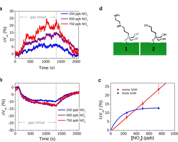
To measure the sensing characteristics of the devices functionalized with amine and thiole SAMs, the respective substrate was placed in a sensing chamber and illuminated through a quartz window to generate the monitored Voc signal. All measurements were performed with samples composed of 16
diodes in series, as they offered the best compromise in terms of signal value and noise level. The test gases were diluted in dry synthetic air (blend of 21% O2 and 79% N2) and applied via a mass flow
controller system into the sensing chamber. Figure 2a shows the response of an amine functionalized sensor towards different concentrations of NO2 (250, 500, 750 ppb). Although the Voc signal showed a
relatively high noise level, a linear increase of the response (ΔVoc) with increasing NO2 concentration
could be observed. Even the lowest value of 250 ppb could be detected with a signal response of ΔVoc = 7.5% and the Voc increased by 23.5% with the introduction of 750 ppb NO2 (see Figures 2 and
5
(typical recovery times were about 5 minutes). The results proof that the device is capable of detecting NO2 in self-powered operation at low ppb values, which is the above mentioned critical range for
environmental monitoring.[10] In sharp contrast to the amine modified device, the response of the thiole
modified device was observed to be negative. An even higher absolute response of ΔVoc = -9.8%
towards 250 ppb of NO2 was achieved for this device. In any case, the increase of sensor response for
the thiole modified samples did not proceed linear with the NO2 concentrations and reached a
saturation value of ΔVoc = -12.8% for 500 and 750 ppb. This characteristic is suitable for highly
sensitive NO2 detection, while a quantitative sensing could not be realized at concentrations >250 ppb
by using the thiole SAM. Remarkably, the inverted sensor signals for the two different organic functionalities prove that the critical gas-surface interactions of the sensor device and consequent electrical modulations are guided by the nature of the SAM molecules. The fact that no response towards NO2 was observed for devices without SAM modification further indicates that the gas-sensor
interaction is solely subsiding by gas-SAM interactions in case of modified samples (see Figure S6), as the incident light (out of the UV range) is not activating direct interaction between ZnO and the surrounding gas atmosphere.[2] Since the illumination with light in the visible range (e.g. natural
sunlight) is sufficient to facilitate gas desorption processes for fast response and recovery processes of SAM modified gas sensors,[7] the organic groups furthermore ensure a sensing operation without the
need of external thermal or UV light energy that is usually required for the activation of the inorganic surface of traditional gas sensor systems and consume a major fraction of the total required energy in conventional sensor systems.
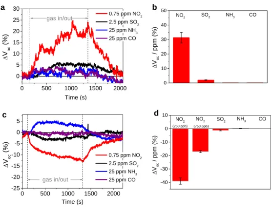
In order to assess the selective sensing capabilities of our devices, we compared the response towards NO2 to common interfering and combustion gases (SO2, NH3 and CO) of significantly higher
concentrations (2.5 – 25 ppm). Figures 3a and b display that the response of the amine functionalized sensor towards all referenced gases is significantly lower than in case of presence of low NO2
concentrations. For 2.5 ppm of SO2, a measurable response of ΔVoc = 5.0% was observed. The
response per ppm of 2.0 %/ppm was remarkably lower than it was observed for NO2 (31.3 %/ppm).
The response of the amine terminated sensor towards 25 ppm of NH3 and CO were just above the
6
revealed a relatively low negative response of ΔVoc = -3.4% towards 2.5 ppm of SO2 (-1.35 %/ppm)
and an increase of the measured Voc by 4.5%, when 25 ppm of NH3 were introduced (0.18 %/ppm)
(see Figures 4b, c, and Figure S7). No signal change was observed after the introduction of 25 ppm CO. The high response towards low concentrations of NO2 (-39 %/ppm for 250 ppb; -17.1 %/ppm for
750 ppb) and a lower signal noise qualifies the thiole modified sensor to be suitable for the selective detection of tiny NO2 concentrations. Nevertheless, the quantitative sensing ability and a higher
response at concentrations above 500 ppb, combined with a very high discrimination of other interfering gas species qualifies the amine functionalized sensor to be more adaptive in real
applications. Besides these promising findings, the stability of the SAM functionalized sensors is still challenging. After exposing the sensors to sequential pulses of NO2 for about 8 hours under constant
illumination, the sensing response was found to be lowered to about 80% of the initial values. Therefore, our ongoing investigations are focusing on the understanding of such degradation processes.
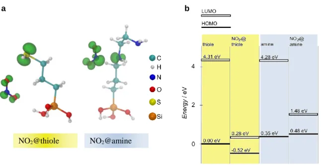
In order to better understand the SAM-gas binding interactions and to evaluate variations of the sensing characteristics between amine and thiole terminated species, theoretical DFT calculations were performed. In order to determine the most stable binding geometries of NO2 for both the amine and
thiole groups 115 different SAM-NO2 configurations with random initial positions and orientations of
the NO2 molecule were relaxed (Figure S8). The thus obtained most stable binding geometries of NO2
with the amine and thiole SAMs respectively are illustrated in Figure 4a. For the amine SAM, NO2
preferably adsorbs near the secondary amine group, where the highest occupied molecular orbital (HOMO) of the SAM is located. For the most stable amine-NO2 geometry the binding energy EB
amounts to -0.44 eV and a considerably high covalent character of the NO2-SAM binding was
observed. Here, more negative values of EB mean stronger binding.
In case of the thiole SAMs the thiole-NO2 binding energy is found to be considerably weaker (EB =
-0.22 eV). For the most stable geometry NO2 adsorbs near the sulfur atom, where the HOMO of the
thiole SAM is located, and additionally forms a weak hydrogen bond with one of the OH groups (Figure 4a). For the thiole-NO2 system some degree of hybridization of the SAM and gas frontier
7
However, here dispersion forces play a more dominant role as compared to the amine case, hence the portion of covalent binding interaction is lower compared to the amine-NO2 system (see supporting
information for further explanation).
Based on these SAM-NO2 binding geometries, we investigated the positions of the energy levels of the
SAM and the most stable SAM-NO2 systems to get an idea about the change of the electronic structure
of the functional groups due to gas adsorption and the differences between the thiole and amine system with respect to the affinity to transfer charges between the SAM-gas system and the ZnO NW. Since the bonding of the amine and the thiole SAM to the ZnO NW in each case occurs most likely via the silicon atom which in both cases has the same chemical environment locally, we chose the average electrostatic potential in the core region of the Si atom of each SAM as common energy reference. Interestingly, we found that NO2 adsorption leads to a downward shift of the HOMO by 0.52 eV in the
thiole case and, in sharp contrast, an upward shift of 0.13 eV in the amine case (Figure 4b). For both systems the LUMO level of the SAM-gas system is much lower than in the NO2 free case. This low
LUMO level is mainly derived from the NO2 LUMO. The DFT calculations thus show that the
electronic structure of the SAM-NO2 system indeed depends on the specific choice of the SAM and is
strongly altered by the NO2 adsorption (shift of the HOMO and LUMO energies). Moreover, the
relatively low position of the thiole-NO2 LUMO (high electron affinity (EA) of the system) and the
relatively high position of the amine-NO2 HOMO (low ionization potential (IP) of the system) indicate a rather electron acceptor character for the thiole-NO2 system and a rather electron donor
character for the amine-NO2 system[19,20]. This is consistent with the experimentally observed reversed
signals of Voc of the thiole and amine functionalized NWs. This relative change of the electron donor
and acceptor character of the organic functionalities upon NO2 binding (change of HOMO and LUMO
energies) could directly influence the electronic structure of the SAM/n-ZnO system and thus,
macroscopically result in a change of the sensor signal (Voc). However, further studies are needed to
better understand the mechanism of the consequent interactions at the SAM-NW interface and the consequent change within the electronic n-ZnO structure.
8
In conclusion, we demonstrated a selective and self-powered gas sensor, capable of detecting low NO2
concentrations in the ppb range without the need of an external power source. The sensor signal (Voc)
was generated by micro-fabricated p-Si/n-ZnO diodes upon visible light illumination. The selective sensing qualities were introduced by functionalization of the n-ZnO surface with amine as well as thiole terminated organic SAMs. Furthermore, the use of an organic SAM facilitated the gas-surface interaction without the need of heat or UV activation, as it is required for bare inorganic gas sensors. Detailed DFT simulations of the SAM-NO2 binding interactions and subsequent changes of the
organic surface group frontier molecular orbitals indicated that the nature of the chemical SAM structure directly determines the gas response of the hybrid material. The contrary relative changes of the ionization potential (IP) and electron affinity (EA) upon NO2 binding for amine and thiole
terminated SAMs correlate well with the experimentally observed sensing results. Therefore, this work gives an insight into the complex sensing mechanism of inorganic-organic hybrid gas sensors and shows the feasibility of transferring chemical signals from specific organic-gas interaction into active electronic signals solely driven by visible light.
Experimental Section
Preparation of serial p-Si/n-ZnO diodes: The p-Si stripes on SiO2 where prepared by
photolithographic patterning of a SOI wafer (Boron doped, R = 1-20 Ωcm) and subsequential reactive etching (RIE) using a mixture of SF6/O2 (129/9 sccm) as process gas (T = -95°C, p = 1.5Pa). For the
site selective growth of ZnO NWs, the etched substrate was again photo lithographically patterned and a 20 nm Zn film was deposited via DC sputtering (99.9999% Zn target, Ar), followed by a resign lift-off an annealing at 300°C in air to form a ZnO seed layer. ZnO NWs were grown by immersing the seeded substrate into a 1:1 solution of zinc nitrate (Zn(NO3)26H2O; c = 0.025mol/L) and
hexamethylenetetramine (c = 0.025mol/L) and stir the solution for 3h at 90°C. After refreshing the solution, the substrate was stirred for another 3h at 90°C. Subsequently, the substrate was removed from the solution, sonicated for 5 s and rinsed for 30 s in deionized water. The Gold contacts were evaporated using photolithographic methods to connect the fabricated single diodes in series.
Preparation of SAM functionalized p-Si/n-ZnO sensors: The as-prepared p-Si/n-ZnO substrates were cleaned in oxygen plasma for 1 min to remove surface contaminations and provide oxygen groups on the surface for the condensation reaction. Subsequently, the sample was immersed in a 1% ethanol
9
solution of [3-(2-Aminoethylamino)propyl]trimethoxylsilane 1(ABCR GmbH) or
(3-Mercaptopropyl)trimethoxysilane 2 (Sigma Aldrich), and was stirred for 3 h. After removal, the sample was subsequently rinsed with ethanol and dried in a vacuum oven for 1 h at 60°C.
Gas sensing experiments: The SAM functionalized p-Si/n-ZnO sensors were electrically contacted via wire bonding and placed in a gas chamber with gas in-, outlet and a quartz window for external illumination. The gas flow was controlled by a flow control system (Gometrics MGP-2) and the Voc
sensor signal was monitored by a SMU (Keithley 2400) that was controlled by self-programmed LabVIEW software (National Instruments Inc.). The sensor was illuminated with a 150 W halogen lamp through a quartz window. All gas sensing experiments were performed at room temperature.
DFT simulations: All calculations were performed within the PBE framework with the Vienna ab-initio Simulation Package (VASP).[22] Here, we used the PAW method and pseudopotentials [23,24] an
energy cutoff of 400 eV and Gaussian smearing with a width of 0.1 eV. For relaxations a force cutoff of 0.01 eV/Å was used. Dispersion forces were taken into account by using the semi-empirical DFT-D2 method of Grimme[25] as implemented in VASP. The geometries of the amine and thiole
functionalities have been relaxed in simulation boxes of the size 13x13x20 Å3. For the evaluation of
the electronic structure properties such as the energy level positions static calculations in simulation boxes with the dimensions 30x30x30 Å3 were used in order to suppress spurious interactions between
neighbouring images. The projection of the HOMO of the SAM-NO2 system onto the molecular
subsystems was performed by a preceding projection onto spherical harmonics centered around the corresponding atoms of the subsystems and the subsequent summation of all contributions.
Supporting Information
Supporting Information is available online from the Wiley Online Library or from the author. Acknowledgements
The authors wish to express their sincere gratitude to J. Arens and A. Schmidt for technical support. The research leading to these results has received funding from the European Research Council under the European Union's Seventh Framework Programme (FP/2007-2013) / ERC Grant Agreement n. 336917.
Received: ((will be filled in by the editorial staff)) Revised: ((will be filled in by the editorial staff)) Published online: ((will be filled in by the editorial staff))
10 [1] Z. L. Wang, Adv. Mater. 2012, 24, 280–285.
[2] M. W. G. Hoffmann, A. E. Gad, J. D. Prades, F. Hernandez-Ramirez, R. Fiz, H. Shen, S. Mathur, Nano Energy 2013, 2, 514–522.
[3] X. Xue, Y. Nie, B. He, L. Xing, Y. Zhang, Z. L. Wang, Nanotechnology 2013, 24, 225501. [4] F. Hernandez-Ramirez, J. D. Prades, A. Tarancon, S. Barth, O. Casals, R. Jimenez-Diaz, E.
Pellicer, J. Rodriguez, J. R. Morante, M. A. Juli, S. Mathur, Alberto Romano-Rodriguez, Adv. Funct. Mater. 2008, 18, 2990–2994.
[5] R. M. Penner, Annu. Rev. Anal. Chem. 2012, 5, 461–85.
[6] B. Esser, J. M. Schnorr, T. M. Swager, Angew. Chem. Int. Ed. 2012, 51, 5752–5756. [7] M. W. G. Hoffmann, J. D. Prades, L. Mayrhofer, F. Hernandez-Ramirez, T. T. Järvi, M.
Moseler, A. Waag, H. Shen, Adv. Funct. Mater. 2014, 24, 595–602.
[8] M. C. McAlpine, H. D. Agnew, R. D. Rohde, M. Blanco, H. Ahmad, A. D. Stuparu, W. A. Goddard, J. R. Heath, J. Am. Chem. Soc. 2008, 130, 9583–9.
[9] W. Yuan, A. Liu, L. Huang, C. Li, G. Shi, Adv. Mater. 2013, 25, 766–771. [10] Directive of the European Parliament and of the Council, 2008/50/EG, EU, 2008.
[11] D. Zhang, Z. Liu, C. Li, T. Tang, X. Liu, S. Han, B. Lei, C. Zhou, Nano Lett. 2004, 4, 1919– 1924.
[12] R. V. Cooney, P. D. Ross, G. L. Bartolini, J. Ramseyer, Environ. Sci. Technol. 1987, 21, 77– 83.
[13] A. E. Gad, M. W. G. Hoffmann, F. Hernandez-Ramirez, J. D. Prades, H. Shen, S. Mathur, Mater. Chem. Phys. 2012, 135, 618–622.
[14] A. Kargar, K. Sun, Y. Jing, C. Choi, H. Jeong, Y. Zhou, K. Madsen, P. Naughton, S. Jin, G. Y. Jung, D. Wang, Nano Lett. 2013, 13, 3017–22.
[15] L. E. Halliburton, N. C. Giles, N. Y. Garces, M. Luo, C. Xu, L. Bai, L. A. Boatner, Appl. Phys. Lett. 2005, 87, 172108.
[16] D. Look, G. Farlow, P. Reunchan, S. Limpijumnong, S. Zhang, K. Nordlund, Phys. Rev. Lett. 2005, 95, 225502.
[17] F. Xiu, Z. Yang, D. Zhao, J. Liu, K. a. Alim, A. a. Balandin, M. E. Itkis, R. C. Haddon, J. Cryst. Growth 2006, 286, 61–65.
[18] A. Janotti, C. G. Van de Walle, Rep. Prog. Phys. 2009, 72, 126501.
[19] A. Ebong, V. Upadhyaya, B. Rounsaville, D. S. Kim, V. Meemongkolkiat, A. Rohatgi, M. M. Al-Jassim, K. M. Jones, B. To, IEEE 4th World Conf. Photovolt. Energy Conf. 2006, 1376– 1379.
11 [20] T. Koopmans, Physica 1934, 1, 104–113.
[21] C.-G. Zhan, J. A. Nichols, D. A. Dixon, J. Phys. Chem. A 2003, 107, 4184–4195. [22] G. Kresse, J. Furthmüller, Phys. Rev. B 1996, 54, 11169–11186.
[23] G. Kresse, Phys.Rev. B 1999, 59, 1758–1775. [24] P. Blöchl, Phys. Rev. B 1994, 50, 17953–17979. [25] S. Grimme, J. Comp. Chem. 2006, 17, 1787–1799.
12 0 10 20 30 0.0 0.5 1.0 1.5 2.0 2.5 Voc (V) Number of Diodes
Figure 1. (a) Schematic description of the device fabrication. Higher magnification of a singular p-n unit composed of p-Si µ-trenches. In a subsequent step the n-ZnO nanowires surface was modified by adding a SAM of functional groups. (b) Scanning electron microscope (SEM) image of a singular p-Si/n-ZnO diode. (c) Equilibrium band diagram of a single p-p-Si/n-ZnO diode including the Au contacts on both terminals (see Figure S3 for more details). d) Linear behaviour of the measured Voc with
increasing number of diodes under illuminated conditions (simulated sunlight; AM1.5). This is due to the series association of the photodiodes. Upon absorption of light in the depleted region of each one of them, electrons (solid green circles) drift to the n-ZnO part while holes are extracted though the p-Si (open green circles).
a
13 0 200 400 600 800 1000 0 5 10 15 20 25 amine SAM thiole SAM I V oc I (%) [NO2] (ppb) 0 500 1000 1500 2000 -30 -25 -20 -15 -10 -5 0 gas in/out V oc (%) Time (s) 250 ppb NO2 500 ppb NO2 750 ppb NO2 0 500 1000 1500 2000 0 5 10 15 20 25 30 V oc (%) Time (s) 250 ppb NO2 500 ppb NO2 750 ppb NO2 gas in/out
Figure 2. Response of the sensors in a self powered operation towards different concentrations of NO2
with a) amine and b) thiole terminated SAM functionalizations. c) Diagram of the ΔVoc response
versus different NO2 concentrations for amine and thiole functionalized devices. d) Molecular
structure of the amine ([3-(2-aminoethylamino)- propyl]trimethoxylsilane 1) and thiole ((3-mercapto-propyl)trimethoxysilane 2) terminated SAMs.
b c
1 2
14 0 500 1000 1500 2000 -25 -20 -15 -10 -5 0 5 V oc (%) Time (s) 0.75 ppm NO2 2.5 ppm SO2 25 ppm NH3 25 ppm CO gas in/out 0 500 1000 1500 2000 0 5 10 15 20 25 30 Voc (%) Time (s) 0.75 ppm NO 2 2.5 ppm SO 2 25 ppm NH 3 25 ppm CO gas in/out
Figure 3. a) Responses of the amine functionalized sensor towards NO2 in comparison tointerfering
species (SO2, NH3, CO) and b) summary of the sensitivity values. c) Comparative responses of the
thiole functionalized sensor and d) summary of the sensitivity values. b d 0 10 20 30 40 50 CO NH3 SO2 Voc / ppm (%) NO2 -40 -30 -20 -10 0 10 (750 ppb) NO2 Voc / p pm (%) CO NH3 SO2 NO2 (250 ppb) a c
15
Figure 4. a) Most stable geometries of a NO2 molecule adsorbed at the thiole and amine functionality
respectively. The charge densities of the HOMO wave functions are shown as green isosurfaces. The isosurfaces are drawn at a value of 0.075 e/Å3. In both cases the HOMOs are hybrids of the HOMO of
the organic functionality and the NO2 LUMO. In the amine case strong mixing between the amine
HOMO and the NO2 LUMO occurs whereas in the thiole case the HOMO of the combined system is
dominated by the thiole HOMO. b) Energy levels of the HOMO and LUMO of the functionalities without adsorbed NO2 and with adsorbed NO2. The averaged electrostatic potential from the core
region of the Si atom of each functionality was used as reference potential. The HOMO level of the isolated thiole functionality was set to 0 for convenience.
a b
NO2@amine
16
Selectivity and low power consumption are major challenges in the development of sophisticated gas sensor devices. In this work we present a sensor system that unifies selective gas-sensor interactions and energy harvesting properties, using defined organic-inorganic hybrid materials. Simulations of chemical binding interactions and the consequent electronic surface modulation give more insight into the complex sensing mechanism of selective gas detection.
Sensors/Biosensors
M. W. G. Hoffmann, L. Mayrhofer, L. Caccamo, O. Casals, F. Hernandez-Ramirez, G. Lilienkamp, W. Daum, M. Moseler, A. Waag, H. Shen and J. D. Prades
Highly Selective and Self Powered Gas Sensor Enabled via Organic Surface Functionalization of p-Si/n-ZnO Diodes
17
Copyright WILEY-VCH Verlag GmbH & Co. KGaA, 69469 Weinheim, Germany, 2013. Supporting Information
for Adv. Mater., DOI: 10.1002/adma.((please add manuscript number))
Highly Selective and Self Powered Gas Sensor Enabled via Organic Surface Functionalization of p-Si/n-ZnO Nanowire Diodes
Martin W. G. Hoffmann, Leonhard Mayrhofer, Lorenzo Caccamo, Olga Casals, Francisco
Hernandez-Ramirez, Gerhard Lilienkamp, Winfried Daum, Michael Moseler, Andreas Waag, Hao Shen and J. Daniel Prades
A. Crystallographic analysis of n-ZnO NWs grown on p-Si substrate
30 40 50 60 10 100 1000 10000 100000 Si (0 0 2 ) Z n O ( 0 1 3 ) Z n O ( 1 1 0 ) Z n O ( 0 1 2 ) Z n O ( 0 1 1 ) Z n O ( 0 0 2 ) In t [ coun ts] 2Theta [°] Z n O ( 0 1 0 )
Figure S1. a) Logarithmic and b) linear plot of the XRD spectrum from ZnO NWs, showing the characteristic reflections of hexagonal ZnO, and of the prominent ZnO (002) reflectance that is indicating an aligned growth along the c-axis, respectively
30 40 50 60 0 2000 4000 6000 8000 10000 12000 Zn O ( 01 2) Zn O ( 01 0) Zn O ( 01 1) Zn O ( 01 3) Si (00 2) Zn O ( 00 2) Int [counts] 2Theta [°]
18
B. Electrical characterization of sensor devices
Figure S2. I-V diagrams of p-Si/n-ZnO devices with a) 9, b) 16 and c) 26 diodes in dark conditions (blue) and under solar illumination (AM1.5). The dotted line depicts the Voc values at I = 0 A. d)
SEM image of a sensor chip with devices of 9, 16 and 26 diodes.
-1 0 1 2 3 -0.05 0.00 0.05 0.10 16 diodes dark 16 diodes solar Current ( µA/c m 2 ) Voltage (V) -1 0 1 2 3 -0.2 -0.1 0.0 0.1 0.2 0.3 0.4 9 diodes dark 9 diodes solar Current ( µA/c m 2 ) Voltage (V) -1 0 1 2 3 -0.02 -0.01 0.00 0.01 Current ( µA/c m 2 ) Voltage (V) 26 diodes dark 26 diodes solar a b c d
19
C. Equilibrium band diagram of the heterojunction structure
Figure S3. Detailed band diagram of one single p-Si/n-ZnO heterojunction including the two Au metal contacts.
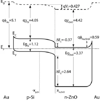
The discontinuity of the conduction (ΔEc) and valence (ΔEv) equation (1) and (2)-, the build in potential (Vbi) -equation (2)-, the depletion width in the p- (XSi) and n-region (XZnO) -equations (4) and (5)-, and the bending of the energy bands (ΔSi and Δ,ZnO) -equations (6) and (7)- [1], where
calculated using the values shown in Table S1 for the impurity concentrations of the p- (Na) and n-type (Nd) materials, the intrinsic carrier concentration (ni), the work function (ϕ), the electron affinity (χ), the band gap (Eg), the equivalent density of states of the conduction band minimum (Nc) and valence band maximum (Nv), and the dielectric constant () of each material.
eV q Ec ( Si ZnO)0.37
(1) eV q E E Ev( g,ZnO g,Si) ( Si ZnO)2.64 (2) eV E E q E E q q qVbi (SiSi)( Si ( f v))( ZnO ( c f)0.427 (3) m N N N N q V X a d a Si ZnO d bi ZnO Si Si 637 . 0 ) ( 2 (4) m N N N N q V X d a a Si ZnO d bi ZnO Si ZnO 009 . 0 ) ( 2 (5)20
qN X eV q q Si Si a x Si Si 0.419 2 2 0
(6)
qN X eV q q ZnO ZnO d x ZnO ZnO 0.008 2 2 0 (7)Table S1. Electron structure properties of p-Si and n-ZnO.
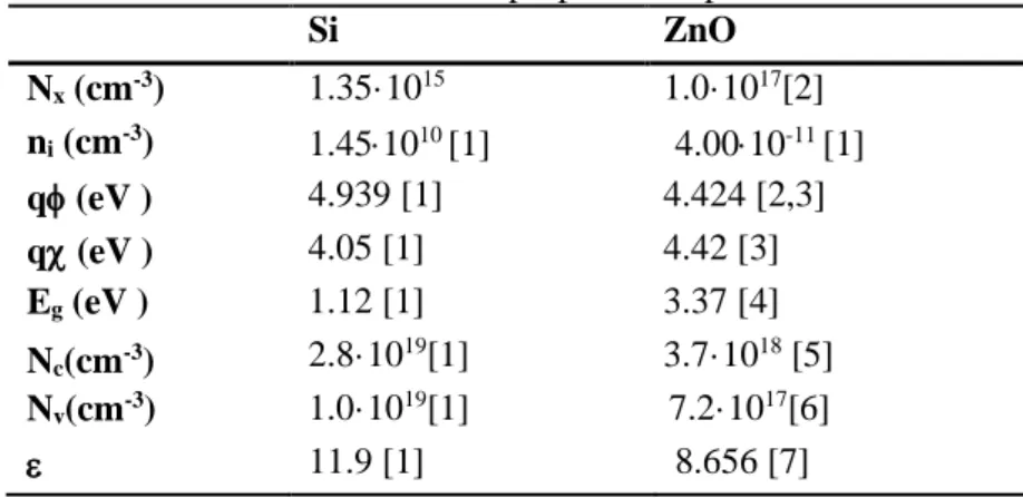
Si ZnO Nx (cm-3) 1.35·1015 1.0·1017[2] ni (cm-3) 1.451010 [1] 4.0010-11 [1] q (eV ) 4.939 [1] 4.424 [2,3] q (eV ) 4.05 [1] 4.42 [3] Eg (eV ) 1.12 [1] 3.37 [4] Nc(cm-3) 2.8·10 19[1] 3.7·1018 [5] Nv(cm-3) 1.0·1019[1] 7.2·1017[6] 11.9 [1] 8.656 [7]
The band bending of ZnO at the ZnO/Au interface was calculated using equation (8), where qAu = 5.1 eV [8] and qZnO = 4.424 eV (see Table S1) are the work function of gold and ZnO,
respectively:
eVq
21
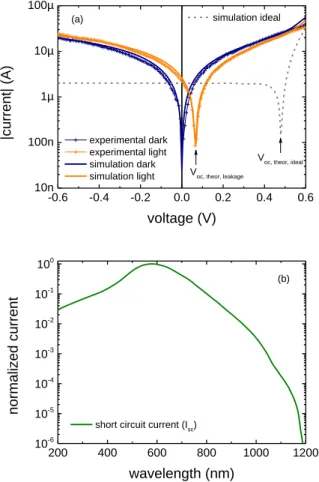
D. Simulation of the optoelectronic device response
-0.6 -0.4 -0.2 0.0 0.2 0.4 0.6 10n 100n 1µ 10µ 100µ experimental dark experimental light simulation dark simulation light simulation ideal
Voc, theor, ideal
|curre
nt| (A)
voltage (V) Voc, theor, leakage (a) 200 400 600 800 1000 1200 10-6 10-5 10-4 10-3 10-2 10-1 100 norm alized curr ent wavelength (nm) short circuit current (Isc)
(b)
Figure S4. (a) Simulated and experimental I/V diagrams of a p-Si/n-ZnO heterojunction with and without illumination considering interface leakage. For reference, the predicted I/V curve for an ideal p-Si/n-ZnO heterojunction is also given. (b) Simulated spectral response of the p-Si/n-ZnO
heterojunctions represented as the normalized short circuit current as a function of the incident photon wavelength.
The electrical behavior of one single p-Si/n-ZnO hereojunction was simulated with PC1D (v5.9), one of the most widely used semiconductor simulators for modeling crystalline solar cells [9].
Our devices were modelled as 1D structures of 10 m and 2.2 m in length for the Si and ZnO parts and a cross section of 7000 m2, in accordance with the real geometry. Each semiconductor was
described by the values given in Table S1. As for the illumination, an AM1.5g source with 0.5 W/m2
of intensity was selected.
The simulations of the band structure in equilibrium lead to results fully consistent with the band diagram shown in Figure S3.
22
First, the I-V characteristic of an ideal heterojunction was calculated, showing remarkable differences with the experimental data. Specifically, a theoretical open circuit voltage in ideal conditions of Voc,theor,ideal = 479 mV/diode was obtained, in big contrast with the experiments
(Voc,exp = 72±6 mV/diode) (see Figure S4.a).
Then, non-ideal effects were included to obtain a more realistic picture of the device performance. In order to account for the leakage current at the p-n interface, attributed to a significant amount of defect induced carrier recombination [10,11], a shunt resistor in parallel with the structure was
considered [12]. Such model successfully predicts the experimental data, with and without
illumination, for shunt resistance values of 30 /cm2. In these conditions, the shape of the I-V curve at
low voltages is more linear and the open circuit voltage is reduced down to Voc,theor,leakage = 68 mV/diode, in accordance with the experimental estimations.
Finally, the spectral response of the device was also modelled, taking into account the light absorption properties of both materials [4]. Figure S4.b shows the spectral response of the device as the
normalized short circuit current at wavelengths ranging from 200 to 1200 nm. This result proves that the structure is suitable for operating in the visible range. In fact, additional calculations of the photogeneration rates along the 1D device axis show that visible photons are collected to generate electron-hole pairs only in the Si region, as expected from its bandgap (Eg,Si = 1.12 eV [1]).
23
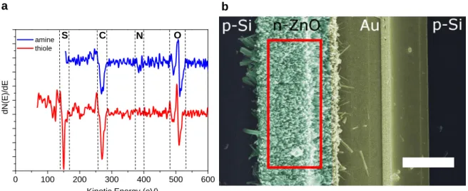
E. Analysis of the organic surface functionalities
Figure S5. a) Auger spectra for amine and thiole modified ZnO NWs showing nitrogen and sulphur signals respectively as well as carbon and oxygen signals for both samples. b) SEM image of a p-Si/n-ZnO device with depicted measurement area on p-Si/n-ZnO NWs. (scale bar: 5 µm)
a b 0 100 200 300 400 500 600 S C N O amine thiole dN(E)/ dE
24 0 5 10 15 20 25 30 CO 25 ppm NH 3 25 ppm SO 2 2.5 ppm V oc (%) NO 2 0.75 ppm -20 -15 -10 -5 0 5 10 CO 25 ppm NH 3 25 ppm SO 2 2.5 ppm V oc (%) NO 2 0.75 ppm
F. Sensing tests for unmodified sensor devices
0
500
1000
1500
2000
-10
-5
0
5
10
15
20
25
30
V
oc(%)
Time (s)
bare ZnO, 500ppb NO2 gas in/outFigure S6. Monitored Voc signal of an unmodified sensor device during a pulse of 500 ppb NO2
Figure S8. Absolute response values of a) amine and b) thiole functionalized sensors towards NO2,
SO2, NH3 and CO.
25
G. Simulation of SAM-gas binding energies and respective HOMO projections
Figure S8. Projection of the HOMO of the SAM-NO2 system onto the NO2 molecule and the SAM
molecules versus the binding energy for all 115 relaxed investigated SAM-NO2 systems. a) The
hybridization of the HOMO of the amine-NO2 system strongly correlates with the binding energy.
This means that for geometries with strong amine-NO2 binding the HOMO extents over both
subsystems. With decreasing binding strength the HOMO more and more completely localizes on the amine. b) Also for the thiole-NO2 system we find that hybridization can occur, as the HOMO extents
over the NO2 and the thiole molecule for the strongest binding energies. However, also relatively
stable configurations do not necessarily show strong hybridization and a localization of the HOMO is found to be majorly on the thiole (dispersive forces are predominant). The covalent character of the thiole-NO2 binding interaction, thus, is less dominant than in the amine-NO2 system.
For the most stable of the considered geometries of the NO2-amine system the site projected HOMO
indicates a considerable hybridization of the amine HOMO and the lowest occupied molecular orbital (LUMO) of the NO2 when forming the HOMO and LUMO of the combined SAM-NO2 system (Figure
S8a). Figure 4a shows the charge density associated with the HOMO of the most stable amine-NO2
system that extends over the LUMO of the NO2 molecule and the HOMO of the amine functionality.
From the strong correlation between this hybridization of amine and NO2 frontier orbitals and the
binding energy of the different relaxed amine-NO2 geometries we conclude that the amine-NO2
binding has a considerable covalent character. Yet, if dispersive interaction forces are neglected, |EB| is
only reduced from 0.44 eV to 0.29 eV for the most stable configuration.
In case of the thiole SAMs the thiole-NO2 binding energy is found to be considerably weaker (EB =
-0.22 eV). For the most stable geometry NO2 adsorbs near the sulfur atom, where the HOMO of the
thiole SAM is located, and additionally forms a weak hydrogen bond with one of the OH groups, Figure 4a. In the thiole case also some degree of hybridization of the SAM and gas frontier orbitals is observed (Figure S8b). However, here the correlation between binding energy and hybridization is less strict than in the amine case. Dispersion forces play a more dominant role here compared to the amine case. Disregarding dispersion forces |EB| is reduced from 0.22 eV to 0.12 eV for the most stable
thiole-a b
NO2 amine
NO2 thiole
26
NO2 geometry, thus, the portion of covalent binding interaction is lower compared to the amine-NO2
system.
In the thiole case also some degree of hybridization of the SAM and gas frontier orbitals is observed (Figure S8b). However, here the correlation between binding energy and hybridization is less strict than in the amine case. Dispersion forces play a more dominant role here compared to the amine case. Disregarding dispersion forces |EB| is reduced from 0.22 eV to 0.12 eV for the most stable thiole-NO2
geometry, thus, the portion of covalent binding interaction is lower compared to the amine-NO2
27
H. References
[1] S. M. Sze, K. K. Ng, Physics of Semiconductor Devices, John Wiley & Sons, New Jersey, 2007. [2] a) L. E. Halliburton, N. C. Giles, N. Y. Garces, M. Luo, C. Xu, L. Bai, L. A. Boatner, “Appl. Phys.
Lett. 2005, 87, 172108.; b) D. Look, G. Farlow, P. Reunchan, S. Limpijumnong, S. Zhang, K. Nordlund, Phys. Rev. Lett. 2005, 22, 225502.
[3] Chiang, T. C., Himpsel, F. J.: 2.1.21 ZnO. Goldmann, A., Koch, E.-E. (ed.). SpringerMaterials - The Landolt-Börnstein Database (http://www.springermaterials.com). DOI: 10.1007/10377019_25 [4] S. Adachi, Properties of Group-IV, III-V and II-VI Semiconductors, John Wiley & Sons, New
Jersey, 2005.
[5] K. Ellmer, A. Klein, B. Rech, Transparent Conductive Zinc Oxide: Basics and Applications in Thin Film Solar Cells, Springer, Berlin, 2007.
[6] Calculated from mh=0.59m0. Ref[3]
[7] S. J. Pearton, D. P. Norton, K. Ip, Y. W. Heo, T. Steiner, Superlattices Microstruct. 2003, 1–2, 3– 32.
[8] D. E. Eastman, Phys. Rev. B 1970, 1, 1–2.
[9] D. A. Clugston, P. A. Basore, Conference Record of the 26th IEEE Photovoltaic Specialists
Conference 1997, 207-210.
[10] F. Xiu, Z. Yang, D. Zhao, J. Liu, K. a. Alim, A. a. Balandin, M. E. Itkis, R. C. Haddon, J. Cryst. Growth 2006, 286, 61–65.
[11] A. Janotti, C. G. Van de Walle, Rep. Prog. Phys. 2009, 72, 126501.
[12] A. Luque, S. Hegedus, Handbook of photovoltaic science and engineering, John Wiley & Sons, New Jersey, 2011.