Abstract—We present the design and simulations of a single-photon sensitive imager based on Single Photon Avalanche Diodes (SPADs) with an innovative pixel architecture that includes 4 separate SPADs with independent active time-gating and quenching circuit, a shared Time-to-Digital Converter (TDC) with 50 ps resolution, 4 independent photon counters, and multiple operation modes. The TDC is driven by smart arbitration logic, which preserves spatial information among the 4 detectors; furthermore, an alternative operation mode exploits photon-coincidence on multiple detectors to reduce the effect of high background levels, e.g. in LIDAR applications with strong ambient light.
Key features are the ability to operate in simultaneous photon counting and timing modes for capturing 2D and 3D images of the scene in a single shot (frame), the option of a counting-only mode, reducing power consumption and increasing achievable frame-rate when timing information is not needed, and the ability to individually shut down noisy detectors or to enable just some regions of interests.
Index Terms—LIDAR; Time-gating; Time-of-Flight; Single Photon Imaging; Smart pixel; SPAD; TCSPC; photon counting.
I. INTRODUCTION
IME-RESOLVED detection of faint light signals in the visible and near infrared region of the spectrum is required by many industrial and scientific applications, ranging from LIDAR (Light Detection and Ranging), surveillance, object tracking, and Time Correlated Single Photon Counting (TCSPC). Silicon Single-Photon Avalanche Diodes (SPADs) are solid-state detectors capable of single-photon sensitivity in the visible and near-infrared spectrum that can be manufactured in a CMOS process, together with on-chip analog or digital circuitry to devise rugged, low-cost monolithic imagers.
Various examples of CMOS SPAD imagers have been presented in literature, with spatial resolution ranging from few tens of pixels up to QVGA, and capable of photon-timing or counting [1]-[5]. None of these imagers can provide simultaneous photon-counting and photon-timing information, which instead can enable smarter time-resolved microscopy and 3D imaging applications. For example, having concurrent 2D and 3D images of the scene eases the task of object recognition and enhances LIDAR capabilities also for moving objects.
The authors are with the Dipartimento di Elettronica, Informazione e Bioingegneria, Politecnico di Milano, Piazza Leonardo da Vinci 32, I-20133, Milano, Italy (e-mail: [email protected]; [email protected]; [email protected]).
II. IMAGER ARCHITECTURE
We present an imager developed in a 0.18 µm high-voltage CMOS technology, which integrates square SPAD detectors with rounded corners (32 µm x 32 µm) in a 32 x 32 array, with 100 µm pitch. The chip layout, shown in Fig. 1, has dimensions of 4.2 x 4.6 mm2 and provides about 1 mm2 of SPAD active area, with a fill factor of 9.6 %. This array is meant to be a test chip for proving its scalability towards the seamless tiling of larger imagers, e.g. 64 x 64 pixels and up to 128 x 128, with minor modifications.
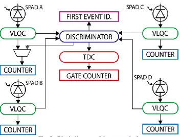
The imager is organized in multi-pixel structures that we devised and called macropixels, each of them with 4 SPADs with independent quenching circuits and photon counters, but sharing one single Time to Digital Converter (TDC) in order to trade-off fill-factor with photon timing performance. Each SPAD is associated with a 23 bit memory cell that stores both the photon timing and photon counting acquisitions. A discriminator circuit preserves spatial information (i.e. the total effective number of laid out pixels, 32 x 32 in this prototype chip) by storing the TDC conversion in the memory cell associated with the triggering SPAD(s). Multiple events can be converted and stored during each frame of acquisition.
III. PIXEL ARCHITECTURE
Fig. 2 shows the macropixel architecture, consisting of 4 SPAD detectors with a gated quenching circuit (VLQC) and a 5-bit event counter each, a shared flash TDC, mode selection
32×32 CMOS SPAD imager for gated-imaging,
photon-timing, and photon-coincidence
Davide Portaluppi, Enrico Conca, Student Member, IEEE, Federica Villa, Member, IEEE
T
Fig. 1. Layout of the designed chip. Dimensions are 4.2 x 4.6 mm2
logic, memory banks and readout logic. This macropixel can operate with multiple gate windows per frame and double buffering to minimize acquisition dead time and maximize duty-cycle. The overall imager operates in global shutter mode.
A. Gated Variable Load Quenching Circuit
SPAD detectors are effectively able to detect photons only when reverse biased above the breakdown voltage of the junction; the difference between the applied bias and the breakdown voltage is called excess voltage VEX. It is thus possible to disable (or “gate-off”) a SPAD by lowering the applied bias voltage below breakdown.
We redesigned our Variable Load Quenching Circuit topology presented in [6], which offers prompt avalanche quenching (thus reducing the circulating charge and the afterpulsing probability) and fast detector reset (250 ps anode fall-time, 20%-80% transition), with the estimated 120 fF capacitance of the SPAD including post-layout parasitics. In fact, in order to perform detector gating, as shown in Fig. 3, we added a PMOS transistor (M4), which disables the detector by pulling the anode voltage up to an intermediate supply voltage (5 V), which must be equal to or higher than the excess bias of the SPAD. In order to re-arm the SPAD, the reset transistor (M1) is activated for about one nanosecond to quickly bring the SPAD above breakdown. M2 is a minimum size transistor, which is kept on while the SPAD is armed. It acts as a dynamic resistor, providing initial passive quenching of the avalanche and making sure that the anode voltage does not drift during the active period. Gated operation is shown in Fig. 4, both in case
of photon detection (blue line) and in case of no detection (red line).
The circuit makes use of thick oxide transistors for sensing, activating and quenching, allowing up to 5V excess bias, in combination with low voltage (1.8V) transistors to reduce area occupation.
A digital counter, clocked by the gate signal, is used to enforce the hold-off time, which is selectable between 0 and 3 gate windows. This ensures that the SPADs exit hold-off condition and are re-armed synchronously to the gate signal. This is highly desirable, because avalanches triggered during the reset transition of the detector are detected with a longer delay than avalanches occurring during the active period, due to the low impedance to ground shown by the reset transistor. This results in distortion of the timing measurement, as any event occurring while the detector is being reset will appear as if it happened at the end of the reset phase, leading to a “pile-up” of detected events at the end of the reset phase. This distortion can be taken into account and possibly corrected only if it is limited to the beginning of the gate window, and it is therefore necessary to avoid its random occurrence across the gate-on period.
If detector gating is not needed, the VLQC can be switched to free-running mode, where the circuit always keeps the SPAD above breakdown unless the detector is in hold-off condition. This greatly reduces dynamic power consumption associated to gating operations. The gate signal is then only used to clock the hold-off counter.
Lastly, a control signal can be used to force the SPAD in its off state, providing a simple way to selectively disable too noisy detectors or to enable only some regions of interest across the array. A distributed shift register addresses each SPAD and shuts unused pixels off.
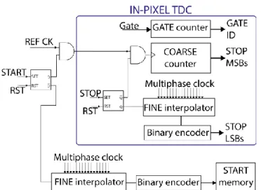
B. Time to Digital Converter
The photon time-tagging scheme, shown in Fig. 5, is based on the Time-to-Digital Converter (TDC) architecture used in [2], which employs both in-pixel and global, out-of-pixel electronics. Both START (synchronous with the laser excitation) and STOP (generated by the macropixel and synchronous with the photon detection in one of the 4 SPADs) Fig. 2. Block diagram of the macropixel.
Fig. 3. Simplified schematics of the gated VLQC. Thick oxide transistors are drawn with a thicker gate.
Fig. 4. Simulated waveforms of the anode voltage during a 10 ns gate-on period without detection of a photon (red line) and with detection of a photon (blue line). Quoted rise and fall times are referred to 20 % - 80 % transitions.
signals are asynchronous with respect to the TDC reference clock, thus implementing the Sliding-Scale technique to improve conversion linearity at the expense of a slightly lower single-shot precision [2] [7]. Furthermore, allowing a START (and STOP) signal asynchronous with respect to the TDC reference clock simplifies the experimental setup, since the LASER can fire at a repetition rate independent from the system master clock.
The timing information is obtained by means of a coarse counter and two fine interpolators, namely the global START interpolator and the in-pixel STOP one. This allows 12-bit photon timing resolution with a nominal LSB (Least Significant Bit) of 50 ps and a 204.8 ns FSR (Full Scale Range). Such FSR is achieved by using an in-pixel coarse counter to extend the limited interpolator range.
Interpolators are made of fast latches, which sample the status of multiphase-clocks generated by a global DLL (Delay Locked Loop) at the rising edge of the input event; then, a thermometric-to-binary decoder generates a 5-bit interpolation result. Simultaneously the 7-bit coarse counter is also stopped.
In an effort to reduce area occupation, routing complexity and overall power consumption, we modified the interpolators to employ both rising and falling edges of the clock phases.
Fig. 6 shows (in a simplified case with just 8 intervals and 4 clock phases) how the reference clock period is subdivided by exploiting both rising and falling edges. For a given LSB and clock frequency, this implementation allows to halve the number of lines to be routed across the chip, strongly reducing power consumption, but introduces a strict requirement on the duty-cycle of the clock phases, which is not a concern in a typical implementation of a multiphase clock interpolator.
To ensure the correct functionality of the TDC, it is mandatory to maintain a 50% duty-cycle of the clock signals, or a large error would appear in the central and last intervals (see Fig. 6), in which the reference edge switches from the rising edge to the falling edge and vice versa, thus causing a large degradation in Differential Non Linearity (DNL) performance. Therefore, we designed the global clock generator circuit to provide clock phases having a nominal 50% duty-cycle.
The clock generator circuit makes use of a 16-tap Delay Locked Loop to obtain 16 equally spaced phases starting from the master clock. These phases are then further interpolated to obtain 32 phases – this is needed to obtain a phase-to-phase time difference lower than the minimum delay that can be achieved by the DLL. The rising edges of phases 0-15 are used to generate the rising edges of the interpolator clock phases, and the rising edges of phases 16-31 generate the falling edges. By doing so, the 16 multiphase clocks (having the same frequency of the master clock) have exactly 50% duty-cycle and a phase shift of 1/32 of the period, subdividing the master clock period in 32 equal intervals. The first 16 intervals are formed by two successive rising edges of the multiphase clocks, whereas the other 16 intervals are given by two successive falling edges.
To ensure that the clocks reaching the pixels have an exact 50% duty-cycle we introduced adjustable-threshold drivers in the clock distribution network, to compensate for voltage drops and mismatches through a slight shifting of rising and falling edges of each clock. A calibration procedure measures the duration of each TDC bin by means of a Code Density test, and then adjusts the buffer thresholds accordingly. In order to speed up the calibration it is possible to combine together the results of all the TDCs connected to the same clock buffers, since an error in the phase offset will affect equally all of them.
Finally, we found that, due to the bus-like structure of the clock routing, crosstalk between adjacent lines is very strong. Due to the capacitive nature of the crosstalk and the deterministic pattern of bus transitions, this effect actually helps in achieving faster rising and falling edges even at the far end of the bus. However, the two outer lines of the clock bus would normally not benefit of this effect, showing significantly softer transitions. It was thus decided to add two guard lines (one at either side of the bus) driven by dummy clock phases. This adds the same amount of crosstalk to the external lines of the bus, obtaining uniform clock transitions for all clock lines.
We designed the TDC to execute at most one conversion in each gate window, and it is possible to have up to 64 gate windows per frame. The conversion time is at most few nanoseconds, thanks to the “flash” architecture, and is essentially given by the propagation delay of the decoding logic and the time needed to store data in the memory bank.
In the proposed architecture, a START pulse is provided at the beginning of each gate window, and its arrival-time (with Fig. 5. Block diagram of the photon timing electronics.
Fig. 6. Simplified representation of the multiphase clock intervals. Underlined in color the two transitions involving different kind of edges, that
are most likely to introduce large errors.
Fig. 6. Simplified representation of the multiphase clock intervals. Underlined in color the two transitions involving different kind of edges, that
respect to the master clock) is stored in a global memory. Each pixel, in addition to the interpolator and coarse counter, features a separate 6-bit gate counter, which identifies (within each frame) the gate number in which the STOP signal triggers the TDC: each in-pixel STOP conversion can therefore be associated to the corresponding global START conversion. This allows to adopt the Sliding Scale technique even in multi-gate operation, simply by designing the global START memory bank as a set of 64 registers where to store 64 START conversions per each frame. Furthermore, it is possible to acquire more TDC conversions per frame, with a duty cycle up to:
𝐷 =64∙𝑇𝐺𝐴𝑇𝐸
𝑇𝐹𝑅𝐴𝑀𝐸 (1)
which can be significantly higher than what could be possible in case of single-conversion if the gate window duration is matched to the TDC FSR. Instead, most photon timing SPAD imagers so far reported are able to perform one conversion per pixel per frame of acquisition, thus limiting the duty cycle of the array to:
𝐷 =𝐹𝑆𝑅𝑇𝐷𝐶
𝑇𝐹𝑅𝐴𝑀𝐸 (2)
Other imagers presented in literature [2] employ out-of-pixel memories, leading to a routing-limited structure which cannot be scaled in dimensions. Conversely, the in-pixel integration of the entire multi-gate logic makes the proposed architecture much more versatile.
In order to allow the 4 SPADs to detect photons in different gate windows, the gate counter is never stopped: instead, its content is latched in the SPAD conversion register when a TDC conversion is triggered.
It is also possible to operate in single gate per frame mode; in this case, conversion rate will be limited to one per frame, but the frame rate can be increased up to 4-fold by changing readout mode, as will be described in Section III-D.
C. Discriminator and mode selection logic
The discrimination logic, shown schematically in Fig. 7, receives the output from each VLQC and controls the TDC triggering and conversion result storage. We conceived multiple operation modes, yielding a versatile structure.
The in-pixel memory is organized in 4 slots of 23 bits each, divided in 18 bits of photon timing information and 5 bits of
photon counting data. Each slot is double-buffered, so that a global FRAME signal latches the working registers’ contents in their output registers, and resets the former for a new acquisition.
In normal operation, a rising edge from one VLQC output triggers the TDC conversion; when this happens, the other SPADs are inhibited from triggering further conversions in the same gate window. The in-pixel memory is organized so that each SPAD has its own memory cell where one timing conversion result is stored. If, by chance, two (or more) events are detected within a fixed coincidence time of about 100 ps, then the result of the conversion is stored in all the corresponding SPADs’ registers. After a SPAD has triggered a conversion, it is inhibited from starting further conversions within the frame, in order to prevent the TDC from converting events which can no longer be stored. In the following gate windows, the other detectors are still able to trigger a conversion, until all memory cells are filled – then, no further conversion can take place until a new frame is started.
A second operation mode is the “first event” mode, where the first TDC conversion of each frame is saved in the register normally belonging to SPAD A. The status of the SPAD outputs that triggered such a conversion (“WHO” in Fig. 7) is saved in a dedicated 4-bit register to avoid losing spatial information. This mode of operation is useful when the conversion rate is expected to be low enough that the probability of a second event per frame is negligible, and reduces the amount of data generated by the array during each frame by a factor of 4, thus yielding a much faster readout and frame rate (see also Section III-D).
The third operation mode is the “two-photons” mode, intended for rejection of background illumination, which trades off spatial resolution for uncorrelated events suppression. In this mode, the TDC conversion is triggered only when at least two photons are detected within a predefined coincidence time window (about 1 ns). This is similar to the method proposed in [8]; unlike their implementation, we fix the coincidence threshold to 2 SPADs, which is the most favorable tradeoff with 4 detectors in each micropixel. Compared to a different approach where the conversion is always triggered by a first photon and saved only if a second photon validates it, our solution avoids wasting TDC conversions for single-photon events, at the expense of saving the timing information of the second photon instead of the first one.
The coincidence logic is made with a set of AND gates fed by every permutation of the 4 signals: we made this choice because of the small number of detectors in the macropixel, though it should be revised if the macropixel structure needed to be expanded to a larger number of SPADs. We implemented a symmetric design and layout in order to reduce the timing skew due to the different relative arrival times of either input of the AND gates. Care has been taken to guarantee that the routing of the outputs of the 4 VLQCs have the same propagation delay, and a Set-Reset latch ensures that partially overlapping events are either converted correctly or discarded. In this operation mode, the memory is remapped in such a way that the first conversion is stored in the register belonging to Fig. 7. Block diagram of the discrimination logic
SPAD A, while the second one is stored in SPAD B’s register, and so on until the 4 slots are filled.
In all these three operation modes, the four in-pixel counters for photon counting measurements are directly connected to the VLQC outputs, with the exception of SPAD A’s counter, whose count input is either the SPAD A signal or the detection of a multi-photon event, depending on whether the discriminator is set in the two-photon mode. The counters are saturating counters, thus avoiding counter folding if illumination gets too intense.
The macropixel can also operate in count only mode. In this case the TDC clocks are shut down, greatly reducing the overall power consumption, and only the registers for counting information are readout, reducing the amount of data and the readout time (see Section III-D).
If low-power consumption is a must, the array can be operated in “software gated mode”, in which the detectors operate in free-running mode, and the gate signal is used in an AND mask with the event inputs, allowing only the events falling within the gate window to trigger a conversion. This allows a selection of the incoming photons, but does not prevent the detectors from being blinded in case of strong incoming light just before the gate-on window. Thus, the choice between hardware and software gate must be carefully selected depending on the specific application.
D. Readout logic
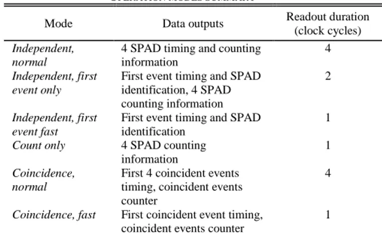
The readout logic (see Fig. 8) allows different readout modes which can be combined with the discriminator modalities to fit the needs of different applications. Complete readout of the pixel requires 4 clock cycles, since each of the 4 memory registers requires a clock cycle to be read, but faster readout modes requiring 2 or 1 clock cycle(s) are provided: readout configuration is performed through three static control signals. An overview of all combinations of operation and readout mode is reported in Table I, with the number of clock cycles required for readout.
Assuming a 100 MHz reference clock and remembering that the readout includes not only the pixels but also the 64 slots of the TDC START memory, a frame-rate higher than 90,000 fps can be achieved in full readout mode, and up to 4 times higher (360 kfps) in fast readout.
All in-pixel memory registers are double-buffered so that it’s possible to perform readout while running a new acquisition. Data in the output registers are latched through a global signal, which also resets the counters and the readout logic at the same time.
Pixels along the same row share a common 23-bit wide output bus by means of tristate buffers, which are enabled only for the pixel whose data is being readout.
In an effort to maximize the scalability of the array to larger sizes we developed a readout scheme that minimizes the routing of time-sensitive signals, by removing the column select signal typically used by similar arrays, and at the same time by increasing the bus pre-charge time for using small buffers.
Each pixel includes a small state machine, clocked by the readout clock, dedicated to handling the shared output bus.
Each pixel acts as a buffer for the readout clock (which is being propagated along the same direction of the output bus) but only after its readout is over. While the pixel is waiting for its own readout, the clock propagation is inhibited.
When the clock reaches an unread pixel, its readout state machine handles the various signals that control internal muxes and switches to output the desired set of data. Simultaneously, the output buffers are enabled and the pixel takes ownership of the bus. Once the readout is finished, the pixel disables its output buffers and allows the clock to propagate to the next pixel, which then begins its readout operations; reset of the state machine is initiated by the same FRAME signal which latches the acquisition data in the output registers.
The row selection is made with a similar arrangement, where 16 tri-state row buffers share an output bus. Each buffer is enabled by a circulating one-hot shift-register that advances at each readout clock cycle, thus enabling one row at a time. The readout clock of each row of pixels, whose frequency in this chip is 1/16th of the master readout clock, is generated by the row’s output buffer itself, which sends a clock pulse to the pixels as soon as the readout of that given row is completed (i.e. the enable signal reaches the output buffer of the following row). By doing so, each pixel has 15 master clock periods available to precharge the row bus before the data is actually read, greatly relaxing readout timing constraints.
This readout scheme is extremely flexible and will allow to design arrays partitioned in many sectors with independent readout without altering the layout of the core, allowing the same macropixel to be used in arrays with different sizes with no need of redesign.
TABLEI OPERATION MODES SUMMARY
Mode Data outputs Readout duration (clock cycles)
Independent, normal
4 SPAD timing and counting information
4
Independent, first event only
First event timing and SPAD identification, 4 SPAD counting information
2
Independent, first event fast
First event timing and SPAD identification
1
Count only 4 SPAD counting
information
1
Coincidence, normal
First 4 coincident events timing, coincident events counter
4
Coincidence, fast First coincident event timing,
coincident events counter
1 Summary of available operation modes with available outputs and readout durations.
IV. CONCLUSION
We presented the complete architecture of a CMOS SPAD imager based on 16 x 16 macropixels, providing 32 x 32 SPADs with both photon timing (photon arrival time) and photon counting (intensity) information. The fill-factor is 9.6 % and the overall active area is 1 mm2; the isotropic pitch allows for future fill-factor improvement by means of microlenses.
The array is being manufactured in a 0.18 µm high voltage CMOS technology that allows to integrate 50-ps resolution TDCs based on multi-phase clock interpolators, obtaining high measurement linearity and frame-rates as high as 360,000 fps.
REFERENCES
[1] M. Gersbach, Y. Maruyama, R. Trimananda, M.W. Fishburn, et al. “A Time-Resolved, Low-Noise Single-Photon Image Sensor Fabricated in Deep-Submicron CMOS Technology”, IEEE J. Solid-State Circuits, Vol. 47 no. 6, pp. 1394-1407, June 2012.
[2] F. Villa, R. Lussana, D. Bronzi, S. Tisa, A. Tosi, F. Zappa, et al., “CMOS imager with 1024 SPADs and TDCs for single-photon timing and 3D time-of-flight”, IEEE J. Sel.
Topics Quantum Electron., Vol. 20, no. 6, pp. 364-373,
Nov-Dec. 2014.
[3] S. Burri, Y. Maruyama, X. Michalet, F. Regazzoni, C. Bruschini, and E. Charbon, “Architecture and applications of a high resolution gated SPAD image sensor”, Opt.
Express, vol. 22, no. 14, pp. 17573-17589, Jul. 2014.
[4] D. Bronzi, F. Villa, S. Tisa, A. Tosi, F. Zappa, D. Durini, et al., “100 000 Frames/s 64 × 32 Single-Photon Detector Array for 2-D Imaging and 3-D Ranging”, IEEE J. Sel.
Topics Quantum Electron., vol. 20, no. 6, pp. 354-363,
Nov-Dec. 2014.
[5] I. Vornicu, R. Carmona-Galán e A. Rodríguez-Vázquez, “A CMOS 0.18μm 64×64 single photon image sensor with in-pixel 11b time-to-digital converter”, International
Semiconductor Conference (CAS), 2014.
[6] D. Bronzi, S. Tisa, F. Villa, S. Bellisai, A. Tosi, and F. Zappa, “Fast Sensing and Quenching of CMOS SPADs for Minimal Afterpulsing Effects”, IEEE Photon. Technol.
Lett., vol. 25, n. 8, pp. 776-779, April 2013.
[7] B. Markovic, S. Tisa, F. Villa, A. Tosi, and F. Zappa, “A high-linearity, 17 ps precision time-to-digital converter based on a single-stage delay Vernier loop fine interpolation”, IEEE Trans. Circuits Syst. I, Reg. Papers, vol. 60, n. 3, pp. 557-569, March 2013.
[8] M. Perenzoni, D. Perenzoni and D. Stoppa, “A 64×64-Pixels Digital Silicon Photomultiplier Direct TOF Sensor With 100-MPhotons/s/pixel Background Rejection and Imaging/Altimeter Mode With 0.14% Precision Up To 6 km for Spacecraft Navigation and Landing”, IEEE J.
Solid-State Circuits, vol. 52, no. 1, pp. 151-160, Jan. 2017.
Davide Portaluppi was born in Magenta, Italy, in 1989. He received the M.Sc. degree (cum laude) in Electronics
Engineering from Politecnico di Milano, Italy, in April 2014. Until October 2015 he has worked on nuclear instrumentation and radiation detectors. He is currently working towards the Ph.D. in Information Technology with Dipartimento di Elettronica, Informazione e Bioingegneria, Politecnico di Milano. His research activity focuses on the design and development of time-gated single photon CMOS imaging arrays.
Enrico Conca was born in Cremona, Italy, in 1992. He received the M.Sc. degree (cum laude) in Electronics Engineering from Politecnico di Milano, Milan, Italy, in September 2016. He is currently working toward the Ph.D. degree in Information Technology with Dipartimento di Elettronica, Informazione e Bioingegneria, Politecnico di Milano. His research activity focuses on the design and development of time-gated single photon counting CMOS circuits.
Federica Villa (M’15) was born in Milano, Italy, in 1986. She received the B.Sc. in Biomedical Engineering in 2008, the M.Sc. summa cum laude in Electronic Engineering in 2010 and the Ph.D. in Information and Communication Technology in 2014, at Politecnico di Milano. Her present research activities include the design and development of CMOS SPAD imagers for 2D imaging via single-photon counting and 3D ranging through direct time-of-flight photon-timing. Since 2015, she is Member of the IEEE. She is co-author of 72 papers.