DOCTORAL SCHOOL
MEDITERRANEA UNIVERSITY OF REGGIO CALABRIA
DEPARTMENT OF INFORMATION ENGINEERING, INFRASTRUCTURES AND SUSTAINABLE ENERGY (DIIES)
PHD IN INFORMATION ENGINEERING
S.S.D. ING-INF/01 XXVII CYCLE
AUTONOMOUS AND ENERGY EFFICIENT WIRELESS
SENSOR PLATFORMS
CANDIDATE
Corrado
F
ELINIADVISOR
P
rof. Francesco G.D
ELLAC
ORTECOORDINATOR
P
rof. ClaudioD
EC
APUAFinito di stampare nel mese di Febbraio 2015
Edizione
Collana Quaderni del Dottorato di Ricerca in Ingegneria dell’Informazione
Curatore Prof. Claudio De Capua
Università degli Studi Mediterranea di Reggio Calabria Salita Melissari, Feo di Vito, Reggio Calabria
C
ORRADOF
ELINIAUTONOMOUS AND ENERGY EFFICIENT WIRELESS
Raffaele ALBANESE Francesco BUCCAFURRI Salvatore COCO Francesco DELLA CORTE Domenico GATTUSO Giovanna IDONE Antonio IERA Tommaso ISERNIA Andrea MORABITO Lorenzo CROCCO Giovanni LEONE Massimiliano MATTEI Roberta NIPOTI Carlo MORABITO Francesco RUSSO Riccardo CAROTENUTO Antonella MOLINARO Maria Nadia POSTORINO Francesco RICCIARDELLI Domenico URSINO Mario VERSACI Giovanni ANGIULLI Giuseppe ARANITI Giacomo CAPIZZI Rosario CARBONE Mariantonia COTRONEI Sofia GIUFFRÈ Fabio LA FORESTA Valerio SCORDAMAGLIA Gianluca LAX Fortunato PEZZIMENTI Giuseppe MUSOLINO Domenico ROSACI Giuseppe RUGGERI Giuseppe SARNÈ Ivo RENDINA Lubomir DOBOS
This work was supported by GELMINCAL project PON 2007/2013: PONa3_00308
I
Contents
Contents ... I List of Figure ... IV List of Table ... VIII
Introduction ... 1
1 Radio Frequency technologies for wireless sensor applications ... 5
1.1 Introduction ... 5
1.2 Radio Frequency Characteristics ... 6
1.3 Wireless Sensors ... 8
1.3.1 Applications ... 10
1.3.2 System evaluation metrics ... 13
1.4 Energy Harvesting ... 16
1.4.1 RF Energy Harvesting ... 18
1.5 Proposed Solution ... 21
2 UHF-RFID Sensor Platform ... 23
2.1 Introduction ... 23
2.2 UHF-RFID Sensor Platform Architecture ... 24
2.3 Rectenna ... 29
2.3.1 Antenna ... 29
2.3.2 Rectifier ... 32
2.4 Impedance Matching in RF Platform ... 34
2.4.1 Modified Friis’s Equation ... 35
2.4.2 Impedance Matching Network ... 36
2.5 Energy Harvesting Performance ... 38
2.5.1 Antenna evaluation ... 38
II
2.5.3 Two stage Dickson Rectifier ... 42
2.5.4 Five stage Dickson Rectifier ... 44
2.6 Dynamic Impedance Matching ... 46
2.6.1 Conceptual approch ... 47
2.6.2 Algorithm ... 47
2.6.3 Measurements ... 49
2.7 Power Management and Digital Section ... 50
2.7.1 Voltage Regulator ... 50
2.7.2 Microcontroller ... 51
2.7.3 RFID Front End ... 52
2.8 Platform Performance Evaluation... 52
2.8.1 Dynamic Impedance Matching Evaluation ... 53
2.8.2 Power Budget ... 54
2.9 Applications ... 55
2.9.1 Wireless temperature sensor ... 55
2.9.2 Performance for Long-run Sensing Applications and Wireless Sensors Networks ... 56
2.9.3 13.56MHz Platform ... 61
2.10 Remarks ... 66
3 CMOS Wireless Sensors ICs ... 67
3.1 Introduction ... 67
3.2 HCPV Monitoring ... 68
3.2.1 System architecture ... 69
3.3 Integrated sensors ... 70
3.3.1 Integrated Temperature Sensor ... 72
3.3.2 Integrated light sensor ... 75
3.3.3 Analog Front End ... 79
3.4 AMS CMOS 0.35μm Analog Sensors ... 82
3.4.1 AMS CMOS 0.35μm Temperature Sensor ... 83
3.4.2 AMS CMOS 0.35μm Light Sensor ... 87
3.5 Digital Section ... 89
3.5.1 Analog-to-digital conversion ... 89
Introduction
III
3.5.3 Load generation ... 90
3.6 RF Section ... 91
3.6.1 LC Cross‐Coupled Oscillator design ... 91
3.6.2 Power Amplifier ... 95
3.6.3 Power On ... 95
3.6.4 On Chip Dipole Antenna ... 96
3.7 Experimental results ... 100
3.7.1 Temperature Sensor ... 100
3.7.2 Light sensor... 103
3.7.3 RF Transmitter performance ... 106
3.7.4 Code Transmission Measurements... 108
3.7.5 Analysis of whole system ... 109
3.8 Remarks ... 110 Conclusions ... 112 Conclusions ... 112 Future works... 114 Acknowledgements ... 115 References ... 116
IV
List of Figure
Fig. 1.1 Block Diagram for wireless sensor node………...………….. 8
Fig. 1.2 Example of a Body Area Network………...……….. 11
Fig. 1.3 Typical application in industrial scenario………... 12
Fig. 1.4 Block diagram of a CMOS RFID tag for environmental monitoring 13 Fig. 1.5 Wearable Thermoelectric Energy Harvesting used for measurements of thermal properties of humans and power generation on people at different ambient conditions……….……. 17
Fig. 1.6 RF to DC converter………... 19
Fig. 1.7 Printed monopole solar antenna………... 19
Fig. 2.1 General block diagram of an energy-harvesting-enabled wireless sensor platform system………... 25
Fig. 2.2 Schematic diagram of α-Wisp battery-free one bit accelerometer (left); photograph of α-Wisp (right)………... 25
Fig. 2.3 Wisp Platform………... 26
Fig. 2.4 Simplified scheme of the designed RFID S-tag ……… 26
Fig. 2.5 RAMSES Platform………... 28
Fig. 2.6 Block diagram of the proposed RFID sensors platform…………... 28
Fig. 2.7 Generic block diagram of a rectenna……… 29
Fig. 2.8 Antenna Field Regions………... 30
Fig. 2.9 Formation and detachment of electric field lines for a dipole……... 31
Fig. 2.10 Schematic of a conventional Dickson multi-stage rectifier………... 32
Fig. 2.11 Voltage Doubler……….. 33
Fig. 2.12 Clamper Effect………... 34
Fig. 2.13 Impedance Matching Network……… 36
Fig. 2.14 Configurations of dual lumped elements matching network……… 37
Fig. 2.15 Monopole Meander………... 39
Introduction
V
Fig. 2.17 (a) λ/2 Dipole antenna; (b) Monopole meander antenna; (c)
Miniaturized antenna……… 40
Fig. 2.18 Evaluation of antenna performances, considering the output voltage of a rectifier connected to the antenna's output……… 40
Fig. 2.19 Input power to rectifier, connected at dipole antenna, estimated through a dedicated power detector………... 41
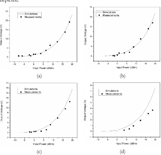
Fig. 2.20 Output voltage of dual the stage Dickson rectifier Vs Input power with 1MΩ (a), 100kΩ (b), 10kΩ (c) and 1kΩ (d) 𝑅𝐿………... 43
Fig. 2.21 Output voltage of the five stage Dickson rectifier Vs Input power.. 45
Fig. 2.22 Efficiency of the five stage Dickson rectifier Vs Input power……. 45
Fig. 2.23 Conceptual approach for dynamic impedance matching…………. 47
Fig. 2.24 Rectifier output voltage Vs Input power………. 48
Fig. 2.25: Input power Vs Rectifier output voltage. The experimental data is compared with the fitting curve……… 48
Fig. 2.26 Experimental prototype……….. 49
Fig. 2.27 Real and Imaginary part of input impedance of the RF energy harvesting circuit at 868MHz……… 50
Fig. 2.28 A snapshot of the prototype connected with a SMA connector….. 53
Fig. 2.29 Energy harvesting efficiency of the realized prototype Vs Input Power. The dynamic matching strategy adopted in this study is compared to the static matching and to no matching options, tested on the same circuit……… 54
Fig. 2.30 A snapshot of the prototype connected with dipole antenna…... 55
Fig. 2.31 24-hour temperature monitoring performed in an indoor environment………. 56
Fig. 2.32 A sample scenario of the network model……… 59
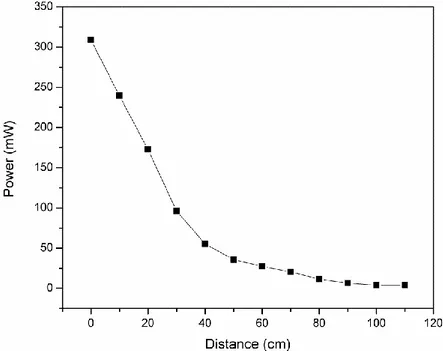
Fig. 2.33 Harvested power varying the distance between the reader’s antenna and the tag……… 59
Fig. 2.34 Number of required readers……… 61
Fig. 2.35 Picture of the 13.56 MHz platform prototype………. 62
Fig. 2.36 Square coil antenna……… 63
VI
Fig. 2.38 Impedance of the smallest antenna on the PCB board with
matching capacitor……… 64
Fig. 2.39 Impedance of the biggest antenna on the PCB board………. 65
Fig. 2.40 Impedance of the biggest antenna on the PCB board with matching capacitor………... 65
Fig. 3.1 Wireless HCPV sensor architecture………... 70
Fig. 3.2 Current driven diode……… 72
Fig. 3.3 Scheme of absolute temperature sensor with matched diode……… 74
Fig. 3.4 BJT biased a different current75 Fig. 3.5 Relationship between absorption length and wavelengths…………. 76
Fig. 3.6 Cross section of photodiode………. 77
Fig. 3.7 Differential pair Amplifier……… 79
Fig. 3.8 Differential pair drain currents versus differential input voltage…… 80
Fig. 3.9 CMOS differential amplifier with PMOS active load……… 81
Fig. 3.10 Transimpedance amplifier configuration………. 81
Fig. 3.11 Wafer section for AMS 0.35μm CMOS Technology………... 82
Fig. 3.12 PTAT with MOS mirror current………. 83
Fig. 3.13 Emitter voltage of transistors Q1 and Q2 at various temperature... 85
Fig. 3.14 Differential output of the PTAT in a temperature range from 0 to 100°C……… 85
Fig. 3.15 Architecture of the integrated PTAT with differential amplifier….. 86
Fig. 3.16 Simulated characteristic of the PTAT Vs temperature……… 87
Fig. 3.17 Structure of realized micro solar cell (top view)………... 88
Fig. 3.18 Simulated Characteristic of the Transimpedance Amplifier vs photocurrent………. 88
Fig. 3.19 Block diagram of Digital Section………. 89
Fig. 3.20 Timing diagram of the start signal generation………. 91
Fig. 3.21 Block diagram of the LC cross coupled transmitter topology…….. 91
Fig. 3.22 Schematic of the ‘cross-coupled’ LC MOS oscillator………. 92
Fig. 3.23 LC Equivalent circuit………. 92
Fig. 3.24 LC cross‐coupled oscillator with CMOS technology……….. 94
Introduction
VII
Fig. 3.26 Structures dipole antennas: (a) linear, (b) zigzag, (c) meander, (d)
loop AMS CMOS Transmitter ……… 96
Fig. 3.27 Simulated frequency carrier of the designed LC oscillator………. 98
Fig. 3.28 Start-up time transient of the designed LC oscillator……… 98
Fig. 3.29 Circuit schematic of the implemented transmitter……… 99
Fig. 3.30 On chip Dipole Cross Section………. 99
Fig. 3.31 Microphotograph of the realized chip……….. 100
Fig. 3.32 Experimental setup used to characterize the PTAT performances 100 Fig. 3.33 Characteristic of the PTAT sensor………... 101
Fig. 3.34 Characteristic of PTAT sensor Vs Supply voltage variations…… 102
Fig. 3.35 Characteristic of PTAT in both directions of operation………... 102
Fig. 3.36 Characteristic of the irradiation sensor under the sun…………... 103
Fig. 3.37 Characteristic of the Transimpedance Amplifier output Vs photocurrent……….. 104
Fig. 3.38 Characteristic of the Transimpedance Amplifier output Vs photocurrent at various temperatures……….. 105
Fig. 3.39 Characteristic of the Transimpedance Amplifier output Vs photocurrent generated by the micro solar cell……… 105
Fig. 3.40 Carrier Frequency of the transmitter………. 106
Fig. 3.41 Phase noise of the proposed transmitter………... 107
Fig. 3.42 Figure Of Merit of the proposed transmitter……… 108
Fig. 3.43 Digital Code and demodulated signal as recorded at the audio output of the radio receiver………. 109
Fig. 3.44 Serialized output of 32-bit PISO………... 109
Fig. 3.45 Digital Code and demodulated signal of recorded at the audio output of the receiver. The data correspond at the light sensor and the PTAT……… 110
VIII
List of Table
Table 1.1 Characteristic of battery………. 10
Table 1.2 Power Density of Energy Harvesting source……….. 16
Table 1.3 ISM frequency bands……… 21
Table 2.1 Synthesizing Reactance (𝑋) and Susceptance (𝐵) using lumped elements……… 38
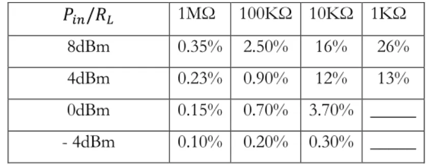
Table 2.2 Measured efficiency of the dual stage Dickson rectifier…………. 44
Table 2.3 Simulated efficiency of the dual stage Dickson rectifier…………. 44
Table 2.4 Sensor platform power consumption under the three operation states……… 55
Table 2.5 Main parameters used in simulation………... 60
Table 3.1 Dimensions of current mirror transistors………... 84
Table 3.2 Transistor dimensions of differential amplifier……….. 86
Table 3.3 Code Table……… 90
Table 3.4 Transistor dimensions of differential cross coupled LC oscillator 97 Table 3.5: Performance summary of proposed LC Oscillator……….. 107
1
Introduction
In recent time, wireless technologies have been rapidly developing, paving the way to the spreading of mobile technologies. Indeed, several
wireless applications grew up for short-range, point-to-point
communications, long-distance cellular phone systems and internet applications.
Moreover, the peculiarity of wireless systems for contactless communications over distance has allowed the development of emerging applications, such as wireless sensor in order to monitor several physical parameters in applications where electro-mechanical systems must interact with the environment. These devices are typically low-cost, low-power and tiny devices, equipped with limited sensing, data processing and wireless communication capabilities, as well as power supply elements.
A far greater potential exists for the development and application of wireless sensors, starting from military or environmental monitoring, moving towards machine‐to‐machine communications (M2M), and eventually reaching all aspects of our lives.
Wireless sensors allow otherwise impossible sensor applications, such as monitoring dangerous, hazardous, unwired or remote areas and locations. This technology provides nearly unlimited installation flexibility for sensors and increased network robustness. Furthermore, wireless technology reduces maintenance complexity and costs.
The link with the RFID technology can be a practical and low‐cost solution to associate Radio Frequency Identification, for tracking of products,
2
animals, or persons, with a dynamic variable data acquisition from on‐board sensors, in order to realize a simple and compact wireless sensor device.
The first solution proposed in this study deals with the development of a wireless sensor platform in RFID technology supervised by a microcontroller (MCU). This approach brings many advantages, in particular the possibility to use the signal transmitted by the RFID reader for harvesting enough energy to make the system battery-less.
This platform, that can be remotely activated and powered, paves the way to a wide range of sensing and monitoring applications. RF fields can be generated on demand, thus providing a more stable and convenient power supply for harvesting system, despite the lower efficiency with respect to sunlight, thermal gradients, mechanical, convection flows or other forms of harvestable energy. Within this scenario, the need for standard battery replacement or maintenance is eliminated.
RF devices that act as sensing nodes can be mounted in positions that are difficult to be accessed by humans, or even embedded within the structure to be monitored during its construction or during the lifetime of artifacts subject to modification of their structure (structural monitoring). The usage of backscattering modulation methods enables the data transmission to be implemented using the same fields that power the nodes.
A simple way to maximize the use of wireless sensors is to reduce the dimensions of transducers and the need of power supply, moving to integrated systems that comprise transducers, logic circuits, an RF oscillator and a radiating element.
Compared to traditional sensors, integrated sensors have the advantage that signal conditioning and interface electronics can be integrated on the same chip. Furthermore, integrating traditional sensors into a chip requires extra fabrication steps and materials, while an integrated sensor can be made in a standard high volume IC process, so production costs can be minimized. In contrast to the classic wired configuration, a wireless communication channel might pave the way to new unexplored applications: the output signal can be transmitted using an antenna realized directly on chip, eliminating the
Introduction
3 need for external transmission line connections and sophisticated packaging, which can radically reduce the cost of IC systems.
Exploiting this technology, the nodes can have sizes of the order of mm3 and be sufficiently inexpensive. Rapid scaling of low cost CMOS technology has enabled circuits and systems to operate into the micro/millimeter wave frequency band, where the required antenna size shrinks and makes the implementation of an on-chip antenna feasible. Thus the on-chip antenna concept is the actual trend in integrated wireless sensor systems because it could be a practical solution to obtain compact, small size and low cost devices for short-range wireless applications.
This thesis is organized in 3 chapters.
Chapter 1 introduces the RF technologies for wireless sensor applications, with a short review of its working principles. Particular attention is addressed at the energy harvesting systems to realize battery-less sensor platforms; finally, RF energy harvesting techniques are discussed.
Chapter 2 describes the RFID wireless sensor platform made with discrete components, that allows to reuse simple and affordable communication protocols and reader systems to acquire sensors data from a macroscopic system. The platform uses an energy harvesting system to supply itself through the RF signal transmitted by a standard reader. In addition the design, implementation and experimental characterization phases, are described. Finally, several applications are presented.
Chapter 3 outlines the wireless sensor in 0.35μm CMOS technology, specifically designed for the monitoring of High Concentration PhotoVoltaics (HCPV) modules. This microchip uses a LC cross-coupled oscillator as RF carrier generator working at frequency of 2.5 GHz, a temperature sensor and a light sensor as transducers. In addition the design, implementation and experimental characterization phases are described.
Conclusions summarize the thesis and conclude with a prediction of future related improvements.
Introduction
5
1 Radio Frequency technologies for wireless
sensor applications
Nowadays, Radio Frequency technologies are key aspects to many electronics fields. RF signals are used as carrier in many systems, as cellular and other wireless technologies including Wi-Fi, WiMAX, NFC, RFID. This chapter introduces the RF technologies for wireless sensor applications, with a short review of its working principles. Particularly attention is addressed at the energy harvesting systems to realize battery-less sensor platforms; finally RF energy harvesting technics are discussed.
1.1 Introduction
Wireless technologies have been growing at an explosive rate over the last few years and have had a significant impact on the information technology industry.
The variety of wireless technologies being developed range from simple IrDA that uses infrared light for short‐range, point‐to‐point communications, to wireless personal area network (WPAN), point‐to multi‐point communications, such as Bluetooth and ZigBee, to mid‐range, multi‐hop wireless local area network (WLAN), to long‐distance cellular phone systems, such as GSM/GPRS and CDMA . Nowadays, the majority of people are
6
aware of the strong impact that these wireless technology products have had mainly due to the astonishing growth of cell‐phone market.
High frequency applications and better reliability of wireless connections are now possible, thanks to the progress of semiconductor technologies and accelerated wireless product development. The products achieved higher levels of efficiency because there is a continued miniaturization of circuitry, displays, user interfaces, the “building blocks” of portable devices, along with advances in low-power electronics and battery (life, weight). For this reason, affordable application solutions are the key ingredient in the rapid acceptance of wireless technologies[1].
Conversely, few people have realized that the demand of bandwidth for wireless, interpersonal communications, such as cellular phones, will soon become a minority share of the total available bandwidth. A far greater potential exists for development and applications of other types of wireless technologies, especially wireless sensors and sensor networks, starting from military and environmental monitoring, moving towards machine‐to‐machine communications (M2M), and eventually reaching all aspects of our lives.
Wireless sensors allow otherwise impossible sensor applications, such as monitoring dangerous, hazardous, unwired or remote areas and locations. This technology provides almost unlimited installation flexibility for sensors and increased network robustness. Furthermore, wireless technology reduces maintenance complexity and costs, although this technology is still in the early stages of development.
1.2 Radio Frequency Characteristics
Wireless technology includes RF (Radio Frequency) systems. The characteristics of radio waves in any frequency band govern how useful those frequencies are for the service necessary. The most significant characteristic, is how signals are transformed or distorted, by absorption and reflection, by the air and other physical objects before reaching the receiver. Some
Radio Frequency Characteristics
7 properties of radio waves can be used to modify the information of the wave. These properties are: wavelength, frequency, amplitude and phase.
RF signals are RF waves that have been modulated to information contain. The behaviors of these signals can be detected and predicted. They propagate differently into different materials and they can interfere with other signals. RF signal behaviors and their implications depend on the following parameters: •Gain •Loss •Reflection •Refraction •Diffraction •Scattering •Absorption •VSWR •Return Loss
•Amplification and Attenuation •Wave Propagation
•Free Space Path Loss •Delay Spread
Antenna is used to transmit and receive the RF signals. An antenna is a passive device, and cannot amplify a signal. It is designed to provide the most efficient method of radiating the signal. The antenna design depends on the signal frequency, the environment in which it is to be used, and the spread of the signal required.
The basic form of antenna is known as the half-wave dipole. It consists of a single element with the feed from the transmitter or receiver at its center. Its length is exactly equal to one half of the wavelength of the signal. Other commonly used types of antennas are: wire, aperture, microstrip, reflector, and arrays. Each antenna has some properties as a radiation pattern and design parameters. The radiation fields of the antenna can be divided into three regions:
8
• Radiating Near Field or Fresnel Region • Far Field or Fraunhofer Region
1.3 Wireless Sensors
Recently wireless devices have been used for sensing applications due to a growing development of transmission and communications interface. Further technologies can be employed for wireless sensors, such as RFID (Radio Frequency Identification) for example. Indeed, a simple ID tag can be integrated with microprocessors, sensory systems, conditioning electronics for realizing a smart wireless device with sensing, computational and communication capabilities. In particular, the combination of RFID technology with sensing systems allows an extension of the application area of smart tags to environmental monitoring, food quality monitoring, home automation and many other applications. Moreover, this device can be employed in networks, named wireless sensor networks, where each smart tag represents a node (Fig. 1.1).
Fig. 1.1 Block Diagram for wireless sensor node
A Wireless Sensor Network (WSN) generally consists of a base station (or “gateway”) which is able to communicate with a number of wireless sensors via a radio link. Data is collected at the sensor node and transmitted to the gateway. The transmitted data are then processed by the system.
Wireless Sensors
9 To satisfy the needs of different application, a modular design approach is usually adopted in order to provide a flexible and versatile system. A memory unit is inserted to allow the node to acquire data from the gateway or when an event happens. In addition, the node is also equipped with a microcontroller, whose flexibility is certainly one of the most important technical features of the device.
A WSN has the potential for many applications: e.g. for military purpose, it can be used for monitoring, tracking and surveillance of borders; in industry for factory instrumentation; in a large metropolis to monitor traffic density and road conditions; in engineering to monitor buildings structures; in outdoor environment to monitor forest, oceans, precision agriculture, etc. Others applications include managing complex physical systems like airplane wings and complex ecosystems [2].
Minimizing the power consumption of wireless sensor nodes is the fundamental problem concerning the design of these devices. Commonly, a large amount of power is required by radio subsystem. For this reason, it is favorable to transmit data only when it is needed. Consequently, a duty-cycled operation of the RF front-end is usually implemented.
Today, batteries represent the principal energy source as regard the node power supply. Thanks to the improvements in battery technology, their energy density with respect to volume and weight (volumetric and gravimetric energy density) has improved by a factor of three in the past 15 years[3]. Table 1.1 shows some typical values of energy densities and self-discharge values for commercial batteries.
A crucial issue is battery lifetime which has up to now limited the diffused adoption of WSNs, where there are a lot of small sensor nodes to power up. Solutions different from standard batteries have been examined, to overcome such restriction. One possibility is to implement energy storage systems that contain a larger energy density. For this reason miniaturized fuel cells represent one promising technology [4].
10
Table 1.1 Characteristic of battery
Battery Type Vol. Energy Density Wh/dm3 Grav. Energy Density Wh/Kg Self-discharge % per year Cycle Life n° Alkaline 300 125 4% 1 Ni-Cd 100 30-35 15%-20% 300 Ni-MN 175 50 20% 300 Li-Ion 200 90 5%-10% 500
Fundamentally, a fuel cell is a power generator that use chemical fuels (i.e. hydrogen or methanol). The gravimetric energy density of these batteries is estimated to be three to five times larger than Li-ion systems. However, the problem of maintenance has not been resolved because these cells need to be refilled of chemical fuels.
Recently, the power supply issue has been limited by energy harvesting systems, which are able to accumulate the necessary power from the environment (e.g. thermal energy, vibrational energy, solar energy or RF radiation). This energy is stored usually in a capacitor and could be used to supply the whole system. However, such an approach enables battery-free operation allowing the deployment of potentially maintenance-free wireless sensor networks and theoretically an infinite lifetime.
1.3.1
Applications
RFID technology is typically and primarily used for identification and tracking purposes. In those application class many tags deployments can be addressed, such as anti-theft, parcel movements and public access areas. However, the increase of tags functionalities, and especially the feasibility of providing RFID systems with sensing capabilities, determines the using area of the smart tags to be enlarged to monitoring applications and their use in the development of wireless sensors. These sensors differ in autonomy, form factor and their configuration, but they all face the same technological objectives such as lifetime, functionality, sizing and costs.
Wireless Sensors
11 For example, wireless sensor is an auspicious technology for health care applications. Recently, sensor network platforms have been used to monitoring the human activity, in order to find various biological and physiological signals. This approach can help solve the longstanding problem of how to infer human activity [5]. Smart tags can be employed for recording, body temperature, for example, in post-operation patients where contactless devices are preferable since they allow an hygienic and non-invasive measurement method (Fig. 1.2). Moreover, long-term monitoring plays an especially important role in improving diagnosis and therapy in modern medicine. Again, smart tags can be applied potentially for the healthcare of elderly people providing monitoring during their daily routines[6].
Fig. 1.2 Example of a Body Area Network[6]
Wireless sensors have been positively used in many industrial applications such as security, control, maintenance, monitoring. A typical usage consists of a collection of sensors, and actuators connected to the central control unit (workstation) using standard RF-links (Fig. 1.3). The sensors are directly connected to the workstation through a RF link.
12
Fig. 1.3 Typical application in industrial scenario [7]
Each sensor or actuator has a reconfigurable wireless or smart sensor interface (SSI). The interface receives data from the sensors, transmits the command to the actuator, and provides a data communication interface to the workstation [7].
Also in the Agriculture-Food sector the development of wireless sensor is emerging. These technologies are very promising in several fields such as environmental monitoring, precision agriculture, cold chain control and traceability [8]. In this contest a demonstration of the system along an intercontinental fresh fish logistic chain have been developed. The usage of wireless sensors presents important advantages regarding conventional traceability tools[9].
Two main applications can be addressed into environmental monitoring: data collection and security monitoring. In both cases smart tags are usually employed over a long period of time at known locations. Therefore, extremely long lifetime devices are required.
In [10] an RF powered transponder with a temperature sensor and a photo sensor is used in environmental monitoring applications. A base station enables the tag that activates the collecting and transmitting of data. In Fig. 1.4 the layout of this system is shown.
Wireless Sensors
13
Fig. 1.4 Block diagram of a CMOS RFID tag for environmental monitoring
[10]
Subsequently, in security monitoring applications smart tags continually monitor the environment, by mean of one or more sensors, to detect an anomaly. With respect to environmental data collecting, each transponder has to frequently check the status of its sensors but it only has to transmit a data report when there is a security violation. Once detected, a security violation must be communicated to the base station immediately. Therefore, in security monitoring applications reducing the latency of an alarm transmission is more important than reducing the energy of the transmissions. This is because alarms are expected to be rare. In a fire security system, for example, alarms would very seldom be signaled. In the event that one does occur, a significant amount of energy could be dedicated to the transmission.
1.3.2
System evaluation metrics
Wireless sensors must have appropriate characteristics in order to fully operate in each application. For example, smart tags should be equipped with transmitters, in data collected applications, that request minimum power in a certain range communication, since data transmission is required at regular intervals. On the contrary, in security applications, transmission section is
14
enabled only when an anomaly is detected, therefore a fast response device is essential.
A set of metrics can be established in order to evaluate the performance of a transponder. These metrics are often interrelated: as a result an improvement in one evaluation metric, e.g. communication range, often comes at the expense of another, e.g. power.
Lifetime
The expected lifetime of smart tags is the key parameter in most applications. Indeed, a long lasting device can be placed out in the field and autonomously work for months or years. The energy supply is the principal limiting factor for the lifetime of such a device.
In some conditions it may be possible to exploit external power. However, the ease of installation is one of the main benefits to wireless systems. Devices that required external power supply, negates this advantage.
Smart tags should be self-powered. They need to contain stored energy to function, or to have the ability to source energy from the environment through external supplies like solar cells or RF generator for example [11]-[12].
Therefore, the main objective of both of these possibilities is that the standard energy use is minimal. Radio power consumption is used to ascertain the lifetime of an energy supply.
When the transmission of output power or radio duty cycle is reduced, power consumption can fall.
Power Consumption
Smart tags need to operate on ultra-low power in order to comply with specific operating conditions. It is possible to achieve a very low power consumption through the combination of low- duty cycle operation methods and low- power hardware. Radio communication makes up a significant percentage of the total energy budget during active operation: therefore radio activity needs to be reduced. When this power is reduced it means that the
Wireless Sensors
15 antenna receives less power and the communication distance is therefore reduced. Consequently, the transmission output power can be lowered.
Communication Range
Besides expected lifetime, coverage is the principle evaluation metric for a wireless system, due to greater communication benefits over a wider area. The distance covered relies on the working frequency and level of power delivered to the antenna. Increasing the power to be injected into the radiating element enhances the radiated power and communication range. When evaluating antenna performance, smart tags used in environmental monitoring applications commonly need an isotropic radiation pattern this is due to the fact that the relative orientation between transponder and base station are not fixed. The increase of the free space loss and, the decrease of the radiated power at given distance and power delivered into the antenna determine the reduction of antenna size at high frequency.
Robustness
It is of paramount importance that smart tags are suitably robust. Therefore devices must be physically robust and contain robust functionalities. This can be achieved by circuit design: for example, the robustness of wireless links to external interference can rise significantly through the use of multi-channel and spread spectrum radios[13]. Monolithic tags enhance robustness against mechanical stress and for smart tags to be utilized in outdoor applications they must be appropriately packaged to minimize atmospheric damage.
Size and Cost
The dimension and market price of a smart tag will obviously have a great impact on its exploitation. Smaller smart tags can be widely used in conventional systems and in various locations. Similarly, cheaper smart tags are more economically viable and accessible.
16
1.4 Energy Harvesting
Ambient energy harvesting is the process where energy is obtained from the environment. Energy harvesting, in general, is the conversion of ambient energy into usable electrical energy.
Energy Harvesting technologies differ in macro e micro scale. Macro-scale systems feed the energy network, typically adding kilowatts or megawatts to the power distribution system. On the contrary, micro-scale technologies scavenge milliwatts or microwatts to supply ultra-low power (ULP) devices. In this way is possible to create a perpetual devices with theoretically infinite lifetime.
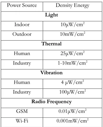
A variety of techniques are available for micro energy scavenging, such as mechanical vibrations, electromagnetic sources, light, acoustic, airflow, heat, and temperature variations. The main differences in these power sources are the power density as shown in Table 1.2.
Table 1.2 Power Density of Energy Harvesting source
Power Source Density Energy
Light Indoor 10μW/cm2 Outdoor 10mW/cm2 Thermal Human 25μW/cm2 Industry 1-10mW/cm2 Vibration Human 4 μW/cm2 Industry 100μW/cm2 Radio Frequency GSM 0.01μW/cm2 Wi-Fi 0.001mW/cm2
Energy Harvesting
17 Solar energy is one of the most commonly used source, featuring high power. The average power density during daytime is about 100 mW/cm2 with
about 20% of average conversion efficiency. In addition a solar panel can also operate in a hybrid mode in conjunction with other types of energy source [14]. The size of a solar panel determine the available amount of power and the values of voltage or current that can be generated. However, large area of solar panel is required to collect sufficient amounts of ambient solar power due to low conversion efficiency of 10%–40%, considering also that its orientation is critical to collect solar power. It is also inefficient on a cloudy day or at night due to the lack of the source.
Another power source commonly utilized is the thermal energy. The temperature difference in thermoelectric devices generates directly electrical power, taking advantage of thermoelectric effects, such as the Seebeck effect or the Thomson effect. As shown in Fig. 1.1Fig. 1.5, an energy density of about 20–60 μW/cm2 is produced by a thermoelectric generator, when it
utilizes the human body as the heat source at room temperature of 18°C– 25°C [15]. Thermoelectric devices can operate continuously as far as there is a temperature difference or a heat flowing across them. The thermoelectric energy-harvesting devices typically need relatively large form factors in terms of volume to generate useful amounts of power.
Fig. 1.5 Wearable Thermoelectric Energy Harvesting used for measurements
of thermal properties of humans and power generation on people at different ambient conditions[15]
18
The piezoelectric effect generates electrical voltages or currents from mechanical strains, such as vibration or deformation. Typical piezoelectric-based energy harvesters keep creating power when there is a continuous mechanical motion, such as acoustic noises and wind, or they sporadically generate power for intermittent strains, such as human motion (walking, clicking a button, etc.). Typical output power density values of usual piezoelectric materials are around 250 μW/cm3 but they can create more
power when a motion or deformation is intense [16]. The piezoelectric energy harvesters or piezoelectric transducers are a well-developed technology, and numerous energy-harvesting modules of this type have been reported [17]. The volume of the piezoelectric power generators is relatively small and light compared to other energy harvesting devices, because a small crystalline structure is able to generate power in these configurations. However, the output power of piezoelectric effect-based power generators has a large dynamic range when irregular motions, such as human motions, are utilized as the driving force.
1.4.1
RF Energy Harvesting
RF energy harvesting involves the usage of external sources of radio frequency waves that are present in the environment, natural radiation, wireless communication, broadcasting etc.
In certain applications radio frequency is the preferred method to power the electronics. Indeed, the huge development of RF communications over the last decades makes RF energy available anytime and everywhere. This energy is virtually in the air, anytime day or night but at differing power levels. The growth wireless technology has brought to a growing interest in RF energy harvesting applications.
The RF energy harvesters system convert directly the RF signal in a DC power (as shown in Fig. 1.6) that can be used to supply ULP systems. RF energy is available in a wide array of frequency bands due to everyday technologies:
•Cell Phones •Radio Towers
Energy Harvesting
19 •WiFi Routers
•Laptops •TV Signals
• Direct RF energy source, dedicated to providing RF energy for harvesting
Fig. 1.6 RF to DC converter
The ambient RF power density is usually higher in downtown urban areas and in the proximity of the power sources (e.g., TV towers) [18].
Ambient RF energy-harvesting systems can be easily integrated with different types of antennas as well as with other harvesting technologies, such as the solar cells[19] Fig. 1.7.
20
It is more challenging due to very low-power-density values and the low RF–dc diode conversion efficiency values to utilize ambient RF power when power harvesters are far away (more than 6 km) from the wireless sources but the harvested RF power can be still utilized by appropriately optimizing the duty cycle of the system (typically below 6%–8%) [20]. The conversion efficiency of RF–dc conversion circuits, such as a charge pump or a rectifier, is about 10%–30% due to low input power levels (from "30 to "20 dBm) but the harvested RF power can generate about 1.8–4.0 V with a total converted power of about 100 μW. This power level is sufficient to operate battery-assisted sensors periodically for a long time (more than five years). The harvested RF power gets larger as the antenna gain and energy density of the ambient environment increase, since the RF–dc conversion efficiency is improved due to the increased input power to the rectifying circuit.
RF harvesting systems rely on a RFID-like approach, in which power is provided to passive tags through the radio waves emitted by a reader. The system realized using this technology is a solution with great flexibility. RF-powered devices can be positioned in inaccessible or dangerous areas, or positions where battery replacement is highly impossible. For this reason, a RF-powered approach was chosen as the best solution for the design of a battery-free wireless sensor.
Wireless sensor nodes, commonly work within unlicensed bands, which are defined as industrial, scientific and medical (ISM) radio bands The telecommunication regulatory authorities states that an unlicensed product user doesn’t need an individual license. However, this differs greatly from unregulated. Wireless devices must follow rigorous regulatory guidelines.
The International Telecommunication Union Radio communication Sector is accountable for radio-communication systems standards and defining ISM RF-powered transceivers for WSNs bands. Below is a Table 1.3
Table 1.1highlighting the frequency range and center of ISM bands [21].
The national radio regulations may produce different frequency bands in some countries.
Proposed Solution
21
Table 1.3 ISM frequency bands
Frequency range Center
frequency 6.765 MHz 6.795 MHz 6.780 MHz 13.553 MHz 13.567 MHz 13.560 MHz 26.957 MHz 27.283 MHz 27.120 MHz 40.660 MHz 40.700 MHz 40.680 MHz 433.050 MHz 434.790 MHz 433.920 MHz 902.000 MHz 928.000 MHz 915.000 MHz 2.400 GHz 2.500 GHz 2.450 GHz 5.725 GHz 5.875 GHz 5.800 GHz 24.000 GHz 24.250 GHz 24.125 GHz 61.000 GHz 61.500 GHz 61.250 GHz 122.000 GHz 123.000 GHz 122.500 GHz 244.000 GHz 246.000 GHz 245.000 GHz
1.5 Proposed Solution
In this thesis, two kinds of wireless sensors with different design strategies have been proposed.
In the first case an autonomous UHF-RFID sensor platform has been realized, using off-the-shelf discrete components. The main advantage of this system is that the communication interface is used for both data collection and energy transfer. In addition, the flexibility of the general purpose microcontroller is certainly one of the most important technical features of the device.
This solution presents several limitations as:
the circuit size, making it a macroscopic object
the need to use discrete components increasing the cost of the finished product
22
over and above to require welding and machining of the PCB. To overcome these obstacles, a second solution has been proposed by trying to achieve a compact, economical and sufficiently accurate system. Researches into related literature were made in order to discover the most advanced solutions. The ambitious objective has been to achieve a wireless sensor that integrates the transducer, the oscillator and the circuitry needed to operate the all in one chip. This microchip has been specifically designed for the monitoring of High concentration photovoltaics (HCPV) modules.
Introduction
23
2 UHF-RFID Sensor Platform
In this chapter a Wireless Smart Sensor Platform, compatible with EPCglobal Class-1 Gen2 readers, is presented. The platform is comprised of a five stage Dickson voltage multiplier, a dynamic impedance matching network (DyIMN), an XLP microcontroller (MCU) and an RFID tag IC with an embedded temperature sensor. Device range operations have been assessed up to a distance of 1.5 m from the RF source, corresponding to a minimum RF input power of -10 dBm. Firmware optimization leads to a reduction of the power dissipation below 500nW in sleep mode, allowing an optimal energy harvesting and storage from the RF source. The harvested power enables logical operations to be completed from MCU, thus enabling sensing and storing of temperature measurements directly into the user memory of an RFID tag. Also the efficiency of the energy harvester is calculated from the MCU, hence tuning the DyIMN dynamically to respond over a wide range of input power and load impedance.
2.1 Introduction
Sensor platforms that can be activated and powered remotely, pave the way to a wide range of sensing and monitoring applications. RF fields can be generated on demand, thus providing a more stable and convenient power supply for harvesting system, despite the lower efficiency compared to sunlight, thermal gradients, mechanical, convection flows or other forms of
24
harvestable energy. Consequently, the need for standard battery replacement or maintenance is eliminated.
RF devices that act as sensing nodes can be mounted in positions that are difficult for humans to be accessed. They can even be embedded within the structure to be monitored during its construction or during the lifetime of the object subject to modification. The usage of backscattering modulation methods enables data transmission to be implemented using the same fields that power the nodes.
Batteryless powered devices are most often used in radio frequency identification (RFID) or passive RF tags [22]-[23] which works within a 1–3 meter range.
The main advantage of sensor platforms that work in the UHF – RFID band is that the communication interface is used for both data collection and energy transfer. Several state-of-the-art platforms [24]-[25] use the signal transmitted by the RFID reader for harvesting the energy, thus enabling a one-way communication from tag to reader.
2.2 UHF-RFID Sensor Platform Architecture
Ambient energy can be harvested from a converter or transducer and then stored inside a storage device, such as a battery or a supercapacitor. Fig. 2.1 shows the general structure of an energy-harvesting enabled wireless sensor platforms. An optimized power consumption can be obtained using a power management unit (PMU) through a desired duty cycle setting. The lifetime of ‘‘main’’ power sources can be improved through the introduction of energy-harvesting systems. Energy harvesting systems can periodically recharge the main power source or operate as an auxiliary source too. It is possible to remove supply power when the harvested energy is enough to supply the whole system. In this case a truly standalone (‘‘battery-less’’) self-powered system is obtained.
UHF-RFID Sensor Platform Architecture
25
Fig. 2.1 General block diagram of an energy-harvesting-enabled wireless
sensor platform system
In recent time, the growth of RFID technology has produced robust systems, capable of wirelessly powering and querying a tag. For this reason, RFID technology allows a new class of wireless, battery-free devices with communication, sensing, computation, and data storage capabilities. Without batteries, these devices can theoretically be operated for an infinite time.
The first developers of UHF RFID tags were Smith et al. in 2005 with their Wireless Identification and Sensing Platform (WISP) realizing the ID-modulation instrument for sensor data transmission [26].
In Fig. 2.2 α-WISP is depicted, it uses two mercury switches to mechanically toggle between two commercially available RFID integrated circuits. The mercury switches are mounted in a geometrically antiparallel configuration, so that when one is open, the other is closed. For this reason, two RFID are necessary to distinguish the different acceleration state.
Fig. 2.2 Schematic diagram of α-Wisp battery-free one bit accelerometer
26
The WISP potentialities have been enhanced by the same authors who, developed the first battery free programmable UHF RFID sensor platform in 2008 [25], as shown in Fig. 2.3.
Fig. 2.3 Wisp Platform[25]
Another low cost general-purpose sensor tag is proposed in [27]. This device can be connected to generic sensors and when it is interrogated by a standard UHF reader, it sends the sensor value through a proper electronic code. In Fig. 2.4 a diagram of the sensor tag (S-TAG) is shown. Here, a generic sensor can be connected at the S-TAG and the measured parameters are transmitted toward the RFID reader by means of a proper set of IDs.
An enhanced UHF RFID tag, realized using inkjet-printing technology on a flexible organic substrate and equipped with a microcontroller and sensors, is proposed in [28].
UHF-RFID Sensor Platform Architecture
27 In [29], one of the first passive UHF RFID humidity sensor tags fabricated using inkjet technology is presented. The sensor tag is based on a RFID integrated circuit (IC) and it operates solely in a passive operation mode.
In [30] a passive multi-standard RFID tag implemented in a 0.13μm bulk CMOS process and enhanced with sensing and localization functionalities is described.
An interesting design strategy for fully-passive RFID sensors is proposed in [31]. Here the change of antenna shape is used to monitor mechanical stress. This sensing mechanism, besides being extremely susceptible to radio propagation phenomena, is not compatible with existing RFID infrastructures. This is due to the fact that it requires expensive equipment, such as vector network analyzers or customized receivers, to reliably extract sensor dependent characteristics from backscattered radio signals.
UHF RFID tag ICs have been developed without internal memory to minimize the cost. UHF RFID tag ICs have been developed without internal memory to minimize the cost. However, the RFID system performances using tags with only unique IDs is restricted in term of transfer data time because of the data search sequence performed in the backend system and the data transfer time between the reader/writer and the backend system . On the other hand, in [32] the design optimization of UHF RFID tag IC with rewritable memory in terms of cost, communication range and transaction time is described.
De Donno et al., in [24] have recently presented the design and performance evaluation of a long-range, self-powered, Gen2-compliant, and programmable RFID sensor platform (RAMSES). The prototype of this platform is shown in Fig. 2.5.
In addition to recent academic research, there are several commercially available Gen2 tags that incorporate sensing, computation, and data-logging capabilities for unconventional RFID applications. For example proposes the SL900A sensor tag [33] available from Austria Micro System, Easy2Log tag by CAEN RFID [34] and the SensTAG by Phase IV [35].
28
Fig. 2.5 RAMSES Platform [24]
A block diagram of the UHF-RFID sensor platform, proposed in this thesis, is depicted in Fig. 2.6. The system is implemented using off-the-shelf discrete components and includes a dipole antenna, a voltage multiplier, a dynamic impedance matching network (DyIMN) [36] a supercapacitor to store the surplus power, an ultra-low power microcontroller (MCU), and a RFID tag IC with an embedded temperature sensor for the wireless communication with EPCglobal Class-1 Gen2 readers.
When the platform enters the RF field of a reader, the rectifier circuit is activated, thus harvesting the RF energy to provide a regulated DC supply voltage (1.8Vdc) to the microcontroller and the tag.
Rectenna
29
2.3 Rectenna
The term “rectenna” derives from the two words rectifier and antenna. It is a device that captures microwave power and instantly converts it into a DC power [37].
A rectenna is composed of an antenna and a diode rectifier circuit, as depicted in Fig. 2.7. The performance of the rectenna depends on its RF-DC conversion efficiency, input power and load values. The conversion efficiency is defined as the ratio of the rectifier DC output voltage and the RF power input on the antenna.
Fig. 2.7 Generic block diagram of a rectenna
Ideally, when using ideal diodes under these circumstances, conversion efficiency would not depend on RF input power. However in reality, it strongly does.
2.3.1
Antenna
An antenna is a metallic device capable of transmitting or receiving electromagnetic wave. The resonance frequency of an antenna is determined by its geometrical characteristics, such as shape and dimension. Common typologies of this radiant element are: wire, aperture, microstrip, reflector, and arrays. Each antenna has some different characteristics of radiation pattern and design parameters.
As shown in Fig. 2.8, the radiation fields of the antenna can be divided into three regions [38]:
Reactive Near Field Region is defined as “that region of the field immediately surrounding the antenna wherein the reactive field
30
predominates.” For most antennas, the outer boundary of this region is given as:
𝑅1 < 0.62√𝐷
3
𝜆 (2.1)
where 𝑅1 is the distance from the antenna, λ is the wavelength and 𝐷 is the largest dimension of the antenna.
The radiating near-field (Fresnel) region is defined as “that region of the field of an antenna between the reactive near-field region and the far-field region wherein radiation fields predominate and wherein the angular field distribution is dependent upon the distance from the antenna”. The region where this region exists, is given by:
0.62√𝐷
3
𝜆 < 𝑅2 < 2𝐷2
𝜆 (2.2)
The far-field (Fraunhofer) region is defined as "that region of the field of an antenna where the angular field distribution is essentially independent of the distance from the antenna". The region where this region exists, is given by:
𝑅 ≥2𝐷
2
𝜆 (2.3)
Rectenna
31
Dipole Antenna
The dipole antenna is the simplest radiating and receiving element, consisting essentially of two symmetrical wires laying on a straight line. If the antenna is made from a single metal branch, it can be defined a monopole that can be directly connected to a coaxial line. It is well known that the basic characteristics of an antenna used for receiving RF signals, such as the gain, the directivity or the impedance, are identical to those calculated when this element is used to radiate an electro-magnetic field, which is the most common approach. For this reason, we will refer to a transmitting antenna in the following.
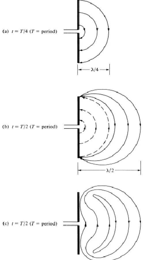
In a dipole antenna, the electric field lines of force are detached from the antenna to form free-space waves[39]. Fig. 2.9(a) depicts the lines of force generated between the arms of a small center-fed dipole in the first quarter of the period. At this point, the charge has reached its maximum value (assuming a sinusoidal time variation) and the lines have traveled outwardly a radial distance λ/4.
32
Assuming that the number of lines formed is three, in the next quarter of the period, the original three lines travel an additional λ/4 (a total of λ/2 from the initial point) and the charge density on the conductors begins to decrease. The reason for this decrease, at the end of the first half of the period, is due to opposite charges that have neutralized the conductor charges. There are three lines of force created by the opposite charges and they travel at a distance of λ/4 during the second quarter of the first half, they are shown dashed in Fig. 2.9(b). The end result is that there are three lines of force pointing upwards in the first λ/4 distance and the same number of lines pointing downwards in the second λ/4. Since there is no net charge on the antenna, the lines of force must have been forced to detach themselves from the conductors and to unite, forming closed loops. This is depicted in Fig. 2.29(c). In the remaining second half of the period, the same procedure is followed but in the opposite direction. After that, the process is repeated and continues indefinitely, forming electric field patterns.
2.3.2
Rectifier
In RF application, the traditional circuit solution adopted for implementing the rectifier stage is based on the Dickson’s topology [40] of the voltage multiplier. In Fig. 2.10, the schematic circuit for this topology of rectifier is shown.
Rectenna
33 Dickson’s circuit performance depends substantially on the voltage threshold of the rectifying devices, which reduces the AC-DC conversion efficiency and sets the minimum input voltage to turn on the circuit. The Dickson’s output voltage, with M+1 pumping devices, can be calculated using the following relation:
𝑉𝑜= 𝑀 ( 𝐶
𝐶 + 𝐶𝑝𝑉𝐴𝐶− 𝐼𝑜
𝑓(𝐶 + 𝐶𝑝)− 𝑉𝑇𝐻) − 𝑉𝑇𝐻 (2.4)
where 𝑉𝐴𝐶 is the peak-to-peak voltage of the AC input signals, 𝐶𝑝 is the
coupling capacitor, C is the parasitic capacitance at each pumping node (not shown in Fig. 2.9), 𝐼𝑜 is the average current drawn by the output load, 𝑓 is
the operating frequency and 𝑉𝑇𝐻 is the diode threshold voltage. According to
(2.4), the following condition has to be satisfied for a positive voltage to be generated at the output:
𝑉𝐴𝐶 > 𝐶 + 𝐶𝑝 𝐶 𝑀 + 1 𝑀 𝑉𝑇𝐻+ 𝐼𝑜 𝑓𝐶 (2.5)
The single stage of the Dickson rectifier is called Voltage Doubler, because the voltage output of this circuit is ideally double compared to the amplitude of the voltage input. As depicted in Fig. 2.11, a Voltage Doubler is formed by a clamper and a single diode rectifier.
Fig. 2.11 Voltage Doubler
The clamper circuit is a combination of the capacitance C1 and the diode D1. The function of this circuit is to shift the continuous component of the sinusoidal input voltage, thus setting its lower extreme at an established value.
34
Fig. 2.12 Clamper Effect
As shown in Fig. 2.12, the input waveform has been shifted in order to put the lower extreme in 0V. This result is obtained assuming that the diode is an ideal device. As a consequence, the amplitude of voltage output is always double compared to the amplitude of input voltage (Voltage Doubler). In reality, the amplitude of voltage output is lower because of the diodes parasitic losses.
Subsequently, the second part of the Voltage Doubler is a single diode rectifier made up of the diode D2 and the capacitor C2. This circuit allows the voltage to be converted into a continuous signal.
2.4 Impedance Matching in RF Platform
Antennas provide different input impedance characteristics due to differences in their geometry, frequency band, and input power. In addition, a rectifier, which converts the AC signal received by the antenna into DC, can have different complex input impedances, depending on its design, fabrication technology and working conditions. As a result, the problem of impedance matching occurs between antenna and rectifier. Here it is necessary to maximize the amount of energy transferred to the load. Correct impedance match between the antenna and the electronics is of paramount importance in RF energy harvesters. In order to obtain the maximum power transfer, the configuration and the component values of the matching network Zin must be determined. Although Zin is not constant during the link
time, several authors propose the matching to a Zin for the longest range as
Impedance Matching in RF Platform
35 optimize the conjugate matching between an antenna with inductive reactive impedance and an integrated circuit with capacitive reactive impedance. Obtaining an antenna with the desired conjugate impedance eliminates the need for an impedance matching network. However, impedance matching can be performed using several other methods including a stub, an inductively coupled loop or nested slot [42]. However, these methods bring further costs and overall increment in system size.
2.4.1
Modified Friis’s Equation
In free-space the power received from an RF antenna, 𝑃𝑎 can be
calculated using Friis’ free-space equation: 𝑃𝑎 = 𝑃𝑡𝐺𝑟𝐺𝑡(
𝜆 4𝜋𝑑)
2
(2.5)
where 𝑃𝑡 is the power transmitted by the reader, 𝐺𝑡 is the gain of the
transmitting antenna, 𝐺𝑟 is the gain of the receiving antenna, 𝜆 is the
wavelength, and 𝑑 is the distance between the reader and the tag.
For RF energy harvesting systems, the rectifier efficiency and the polarization loss shall be taken into account, reducing the effective power delivered to the load.
In [43] Shibo He et al. proposed a modification of (2.5) that describes the power delivering mechanism to a wireless platform better:
𝑃𝑎 = 𝑃𝑡 𝐺𝑟𝐺𝑡𝜂 𝐿𝑝 ( 𝜆 4𝜋(𝑑 + 𝛽)) 2 (2.6)
where 𝐿𝑝 is polarization loss, 𝜂 can be referred to as the rectifier efficiency,
and 𝛽 is a parameter to adjust Friis’ free space equation for short distance transmission.
If the threshold power necessary to power up the electronic load is 𝑃𝑡ℎ,
then the read range 𝑑 can be calculated as (2.4)-(2.5):
𝑑 = 𝜆
4𝜋√
𝑃𝑡
36
The factor:
𝜏 = 4𝑅𝑙𝑜𝑎𝑑𝑅𝑎
|𝑍𝑙𝑜𝑎𝑑+ 𝑍𝑎|2 ≤ 1 (2.7)
is the power transmission coefficient, which accounts for the impedance mismatch between the antenna (Za=Ra ± jXa) and the electronic load (Zload=Rload ± jXload). Both Za and Zload are frequency dependent. In addition, the load impedance also depends on the input power.
The antenna is usually matched at the minimum threshold power level necessary for the electronics to power up.
The amount of power 𝑃𝑙𝑜𝑎𝑑 that can be absorbed by the electronics
from the antenna is given by:
𝑃𝑙𝑜𝑎𝑑 = 𝑃𝑎𝜏 (2.8)
Consequently, to maximize the amount of power transferred to the electronic load, the transmission coefficient must be maximized.
2.4.2
Impedance Matching Network
An impedance matching network can be inserted between the antenna and the electronic circuit in order to provide the maximum power to the load (Fig. 2.13).
Fig. 2.13 Impedance Matching Network
The usage of inductors and capacitors in series or parallel topology is quite common in an impedance matching network, because these passive elements do not dissipate power and do not add noise to the circuit, while active devices do.
Impedance Matching in RF Platform
37 In RF platforms a dual lumped matching networks are commonly used [24]-[25]. This type of network can be realized through two configurations, where the choice depends on the values of Za and Zload.
In the first case, if 𝑅𝐿𝑜𝑎𝑑 > 𝑅𝑎, the configuration depicted in Fig.
2.14(a) must be chosen.
(a) (b)
Fig. 2.14 Configurations of dual lumped elements matching network
In this case, the value of Reactance (X) and Susceptance (B) are calculated as following: 𝑋 = −𝑋𝐿𝑜𝑎𝑑± √𝑅𝐿𝑜𝑎𝑑(𝑅𝑎− 𝑅𝐿𝑜𝑎𝑑) + 𝑅𝐿𝑜𝑎𝑑 𝑅𝑎 𝑋𝑎2 (2.9) 𝐵 = 𝑅𝑎− 𝑅𝐿𝑜𝑎𝑑 𝑅𝑎𝑋𝐿𝑜𝑎𝑑+ 𝑅𝐿𝑜𝑎𝑑𝑋𝑎+ 𝑅𝑎𝑋 (2.10)
In the second case, if 𝑅𝐿𝑜𝑎𝑑 < 𝑅𝑎, the configuration depicted in Fig.
2.14(b) shall be considered .
In this case, the value of Reactance ( 𝑋 ) and Susceptance (B) are calculated as follows: 𝑋 = 𝑋𝑎± √𝑅𝑎(𝑅𝐿𝑜𝑎𝑑− 𝑅𝑎) + 𝑅𝑎 𝑅𝐿𝑜𝑎𝑑 𝑋𝐿𝑜𝑎𝑑2 (2.11) 𝐵 = 𝑅𝑎− 𝑅𝐿𝑜𝑎𝑑 𝑅𝐿𝑜𝑎𝑑𝑋𝑎+ 𝑅𝑎𝑋𝐿𝑜𝑎𝑑+ 𝑅𝐿𝑜𝑎𝑑𝑋 (2.12)
The choice of which passive component to implement in the network depends on reactance and susceptance values. Considering a RF signal with a