Phd Course
Photonic Technologies
Photonics-assisted RF Receivers
for Electronic Support Measures
Author
Daniel Onori
Supervisor
Contents
List of Figures List of Tables Abstract Preface1. Scenario and motivations 6
1.1. Wideband RF systems
1.1.1. Ultra-wideband and multiband radar/communication systems 1.1.2. Electronic support measure receivers
1.2. RF systems based on photonics
1.2.1. Ultra-wideband/multiband transmitters and receivers based on photonics 1.2.2. Microwave photonics receivers for Electronic Support Measures
2. Microwave photonics for RF systems 17
2.1. Electrical-to-optical conversion 2.1.1. The semiconductor laser 2.1.2. The Mach-Zehnder modulator 2.2. Optical-to-electrical conversion
2.2.1. The photodiode
2.2.2. Optical direct detection 2.2.3. Optical coherent detection 2.3. Multi-frequency optical sources
2.3.1. The mode-locked laser
2.3.2. Cavity-less optical frequency comb generators 2.4. Injection locking of semiconductor lasers
2.5. Microwave photonics broadband architectures
3. Photonics-based RF scanning receiver 37
3.1. RF scanning receiver exploiting optical filtering and sampling 3.1.1. Working principle
3.1.2. Simulative study
3.1.3. Experimental setup and results 3.1.4. Discussion
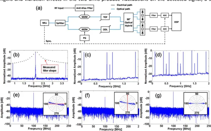
3.2. RF scanning receiver exploiting an optical filter-free direct-conversion architecture 3.2.1. Working principle
3.2.2. Experimental results 3.2.3. Discussion
3.2.4. Improvement in environmental stability: proposal and validation
3.2.5. Realization and laboratory characterization of a 0.5 – 10.5 GHz demonstrator 3.2.6. Field trial characterization
4. Photonics-based 0.5 – 40 GHz software-defined RF signal generation 67 4.1.1. Working principle
4.1.2. Laboratory implementation and results 4.1.3. Discussion
5. Coherent multi-frequency LIDAR for range and Doppler measurements 73 5.1.1. Motivation and state of the art
5.1.2. Working principle 5.1.3. Experimental results 5.1.4. Discussion
6. Characterization and field trials of a photonics-based radar system 84 6.1.1. Introduction
6.1.2. System description 6.1.3. In-field experiments 6.1.4. Discussion
7. Conclusions 91
List of Publications, Awards and Patents 95
Bibliography 98
Abstract
Photonics-assisted RF receiver architectures have been proposed, studied and designed. The innovative solutions exploit photonic techniques to perform a wideband scanning of the RF input spectrum avoiding bulky multiple crystal oscillators and bandpass filters, enabling the solution to overcome the size, weight and power bottleneck that faces pure electronics-based counterparts. The developed demonstrator shows an operating of 0.5÷28.5 GHz, limited by laboratory constraints, and simulative analysis ensures exceeding the 0.5÷40 GHz goal by simply employing commercially available electro-optical devices accepting higher RF driving voltages. The architecture can exhibit an instantaneous bandwidth of several GHz, with linear dynamic range of 160 dB/Hz, spurious-free
dynamic range of 109 dB/Hz2/3,second order input intercept point of 57 dBm, and a measured DC
offset lower than 50 µV. Field-trial campaign results, from relevant Electronic Support Measures scenarios, have been presented, too. Stemming from the same photonic architecture, an innovative software-defined and filter-free RF transmitter has been also proposed and validated. Photonic integration, which is already taken into account, will enable chip-scale solutions with improved performance and environmental stability.
Preface
This dissertation provides a concrete example of the advances photonics can bring about to radio frequency and millimeter-wave systems. The here-presented work tries to be a substantial contribution to the future realization of wideband wireless apparatus able in observing electromagnetic scenarios that span from 0 to 100 GHz and beyond, and fitting in a chip-scale package at the same time.
Nowadays, ultra-wideband/multiband architectures are more and more required in applications like spectrum sensing for cognitive radio, signal intelligence, electronic support measures, and radars. Basically, these challenging systems resort to a stackable implementation of different up/down-converters that cover adjacent portions of the whole spectrum under analysis. Moreover, each converter is usually based on multiple stages, each of them composed by filters, mixers, and oscillators. As a result, the final footprint fits in a rack/cabinet and precludes any applicability in size, weight, and power constrained scenarios as in aircrafts, spacecrafts, unmanned aerial vehicles, etc. What we propose here is a scanning approach using a single widely tunable stage, based on photonics, that avoids any bulky components as microwave filter banks, synthesizers, crystal oscillators, switches, but also DC blocks and complex calibration circuitry, thus permitting a plain on-chip integration. A similar approach results totally unfeasible for current electronic and microwave technologies, essentially due to lack in tunability and performance stability throughout the required operating bandwidth. Instead, photonic technology offers small footprint optical components, as lasers, filters, modulators, hybrid couplers, photodiodes, etc., that present large tunability (hundreds of GHz) and operating bandwidth (100 GHz and beyond), easily enabling a fast scanning architecture. Moreover, photonic integration is rapidly growing, producing photonic integrated circuits more and more robust, reliable, compact, and at lower cost.
The proposals, designs, and experimental work reported in this thesis brought to the realization of a working demonstrator of Photonically-enabled RF scanning receiver, and a world-wide patent, developed in collaboration with Elettronica S.p.A., one of the European leaders in the production of Electronic Defense equipment. Experimental results are obtained with the receiver demonstrator in a relevant field-trial campaign, carried out with the support of the Italian Navy, where typical operative electromagnetic scenarios, characterized by complex threat signals with low-probability of intercept, have been emulated and acquired.
Stemming from the same optical filter-free architecture, an innovative software-defined RF transmitter has been also proposed and validated, demonstrating the same advantages and performance of the receiving solution. Finally, two chapters are dedicated to the presentation of a proposal and demonstration of “Coherent multi-frequency LIDAR for range and Doppler measurements”, and to the characterization and field trials of a photonics-based radar system, respectively, which are two side topics conducted by the author during the Ph.D. programme.
This work is organized as follows:
Chapter 1 is divided in two parts. The first part (section 1.1) gives an overview of the current scenario, state of the art, and perspectives of RF systems for broadband applications, while the second part (section 1.2) takes into account the photonics-based state-of-the-art counterparts.
Chapter 2 provides the theoretical framework needed to understand the photonics-based solutions reported in the following chapters, and illustrates the structure and the working principle of some typical optical devices employed in the experimental activities presented in this thesis.
Chapter 3 introduces the “RF scanning receiver exploiting optical filtering and sampling” (section 3.1) and the “RF scanning receiver exploiting an optical filter-free direct-conversion architecture” (section 3.2) electronic support measures proposal solutions.
Chapter 4 presents the proposal and validation of an innovative software-defined and filter-free RF transmitter.
Chapter 5 is dedicated to the presentation of a proposal and demonstration of “Coherent multi-frequency LIDAR for range and Doppler measurements”.
Chapter 6 is focused on the presentation of a field trials of a photonics-based radar system.
Chapter 1
Scenario and motivations
1.1 Wideband RF systems
Multifunctional radio-frequency (RF) systems, capable of performing adaptive communications, radar, and electronic warfare functions, are of particular interest to both the civilian and military fields. These architectures are enabled by software-defined multiband transmitter and receivers (transceivers) that simultaneously operate at several filtered bands [1].
Moreover, also the instantaneous bandwidth (i.e., the spectrum portion that is instantaneously exploited) of these systems is continuously increasing, embracing ultra-wideband (UWB) functionality [2]. In UWB technology, employed signals present a bandwidth exceeding 500 MHz or 20% of the center frequency, whether they are pulse-based, aggregation of narrow band carriers (e.g. in multiband orthogonal frequency-division multiplexing – MB-OFDM), etc. [2].
Another prominent field of interest, in RF technology, is constituted by full-spectrum receivers, that provide truly continuous coverage of reception of RF signals in a frequency range extending from about 2 to 18 GHz, with a trend to extend the range to 0.5-40 GHz [3,4]. These systems are primarily used in Electronic Support Measure (ESM) applications, where they detect and identify the threats posed by hostile radars (as radars for searching, targeting, tracking, etc.). Since radar menaces use signals with reduced spectral profile (i.e., low power density) for lowering the probability of being intercepted, threat recognition and sorting is becoming more and more difficult. No a-priori hypotheses can be made about the nature of the signals that may be detected, thus high performance is required for adequate reconstruction of the electromagnetic scenario [4].
In Sections 1.1.1 and 1.1.2, the state of the art and current issues of Ultra-wideband/multiband transceivers, and Electronic Support Measures receivers are described, respectively.
1.1.1 Ultra-wideband and multiband radar/communication systems
The main functions of modern multifunctional radar systems are search, track and recognition, but also communication [5]. Currently, these functions are executed either by separate systems that
operate in different frequency bands. On the other hand, future air defense radar trends were addressed by RTO NATO study [6] which concluded that the maximum benefit will be gained from fusion of data (or signals) from multiple radar bands. For example, merging high frequency radar with low frequency radar would yield the best of both worlds assigning the search task to the low frequency radar while enabling the high frequency more accurate sensor to spend more time on target, and thus achieve comparable detection ranges [5]. This is valid under the assumption of equal detection probabilities for both radar. The detection probability is influenced by many factors that are difficult to consider together. The most reliable way of obtaining probability of detection figures for radars in different bands in real situation is co-located simultaneous multiband measurements. The radars being used in the co-located simultaneous multiband radar trials have widely different features and the results are thus difficult to compare. A solution is exploiting a single radar sensor that operates in multiple radar bands [6].
Therefore, multifunctional radar/communication systems require challenging performances, in terms of hardware and software capability, in order to adapt to the scenario under operation. For example, they require reconfigurable and software-defined RF transceivers, capable of generating and detecting radar waveforms over carriers ranging up to the millimeter waveband (MMW, above 30GHz), while maintaining the phase stability necessary for coherent radar applications [7]. At the same time, there is a continued desire to reduce the system size, weight, power (SWaP), and cost. Unfortunately, these architectures currently exploit a stackable implementation that rises the SWaP consumption, thus limiting the applicability in low payload scenarios as aircrafts and unmanned aerial vehicles [6].
In these systems, the exploitation of UWB capabilities can further enhance the performance of both the radar and communication tasks. In the communication field, various UWB systems, that operate in the 3.1 – 10.6 GHz unlicensed band, have been presented due to their benefits in term of high data rate, robustness to propagation fading, interference rejection, and coexistence with narrow band systems [2,8]. Concerning advanced UWB radar system (able to determine a time-frequency signature of the targets), transceivers exploit a wide variety of digitally controlled waveforms in different frequency ranges (multiband operation), tailored to the type of target of interest, offering additional advantages such as superior obstacle penetration, cover operation, resistance to jamming, etc. [9]. Also in this case, such functionalities are introduced at the expense of increased SWaP.
In conclusion, modern multifunctional radar/communication features require multiband/ultra-wideband systems able to provide frequency agility, flexibility, and reconfigurability on the one hand and to optimize size, weight, and power on the other.
1.1.2 Electronic support measure receivers
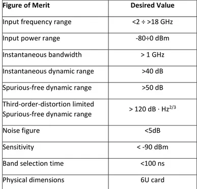
In defense and signal intelligence, electromagnetic sensing is provided by Electronic Support Measure (ESM) systems, which are used to detect and identify the threats posed by potentially hostile radars in complex and dense scenarios [4]. Today’s radar menaces cover the wide frequency range 2-18 GHz (with a trend to extend the range to 0.5-40 GHz [4,5]), and make use of complex signals for performing multiple tasks simultaneously. Therefore, the threat recognition is becoming more and more complex [10]. For this kind of receivers, the most important parameters are the total spectrum range of analysis (or frequency of operation), the instantaneous bandwidth (i.e., the spectrum portion that is instantaneously digitized and analyzed), the sensitivity (i.e., the minimum detectable signal), the instantaneous dynamic range (i.e., the capability of discriminate a weak signal from a strong one), and the spurious-free dynamic range (SFDR) (i.e. the response fidelity of the receiver). In more detail, in [11], the Defense Advanced Research Projects Agency (DARPA) states that “the next generation of multifunctional (ESM, radar, communication) receiver technology will require substantial gains in several key performance parameters, including increased frequency of operation (> 18 GHz), increased instantaneous bandwidth (> 1 GHz), increased spurious-free dynamic range (> 120 dB ∙ Hz2/3) and enhanced receiver sensitivity (< -90 dBm)”. Furthermore, they
Figure of Merit Desired Value
Input frequency range <2 ÷ >18 GHz
Input power range -80÷0 dBm
Instantaneous bandwidth > 1 GHz
Instantaneous dynamic range >40 dB
Spurious-free dynamic range >50 dB
Third-order-distortion limited
Spurious-free dynamic range > 120 dB ∙ Hz2/3
Noise figure <5dB
Sensitivity < -90 dBm
Band selection time <100 ns
Physical dimensions 6U card
declare a continued desire to reduce the system size, weight, power, and cost. Table 1 summarize the main specifications for the next-generation ESM receivers.
Radar warning receivers (RWRs) are the fundamental ESM systems [4,12]: they must show a very high probability of intercept (POI), with low size, weight and power consumption (SWaP) to also meet the needs of requiring applications as the aircraft defense. Current RWRs are typically based on a set of crystal video front ends that analyze adjacent sub-bands covering the range 2-18 GHz to detect the presence of signals (Fig.1.1-A). The sub-bands are separated by a compact, low performance filter bank. Crystal video receivers reach a POI = 1, but they show poor sensitivity, and lack in distinguishing simultaneous signals in the same sub-band. Therefore, in the increasingly complex electromagnetic scenarios, hybrid ESM systems combining the simple and reliable RWR for immediate detection, with a more sophisticate receiver for threat recognition have been recently proposed [5]. The additional receiver should show much better sensitivity and frequency selectivity than the RWR, at the expense of a lower POI.
A candidate, with better sensitivity and frequency resolution but much lower POI, is the ultra-wideband super-heterodyne receiver (Fig.1.1-B), that has an instantaneous bandwidth (BW) of 1-2 GHz and is tunable in the 2-18 GHz range [4,5]. Unfortunately, current local oscillators (LOs) and image reject filters suffer very limited tuning capability, spoiling the applicability of this scanning implementation. In fact, its practical implementation requires multiple bandpass RF filters with sharp skirts (for image rejection), and multiple RF local oscillators to cover the full operative band
Fig.1.1 Scheme of principle of the main receiver architecture for Electronic Support Measures.
Superheterodyne receiver Wide-open crystal video receiver
A cq ui si ti on A) B) C) D) A cq . A cq ui si ti on Superhet Superhet Superhet Superhet Channelized receiver Crystal Video Crystal Video Crystal Video Crystal Video A cq . I/Q Mixer
Direct conversion receiver
Mixer
~
LO
~
LO
Low pass filters Compact RF filter bank
High performance RF filter bank Tunable
[3]. Moreover, in order to reduce the susceptibility to interference and spurs due to the wide instantaneous BW, it must include a second conversion stage with a narrower bandwidth [4]. Therefore, this approach considerably increases the final SWaP.
On the other hand, direct conversion receivers (DCRs) avoid the use of image-reject filters, exploiting instead in-phase/quadrature (I/Q) mixing and low pass filtering, resulting in a reduced complexity with respect to the heterodyne architecture [13] (Fig.1.1-C). Nevertheless, the mixers induce flicker noise, finite port-to-port isolation (LO-to-RF leakage and RF-to-IF feedthrough), and second order intermodulation distortion (IMD2), that result in detrimental DC offset and spurious signals at baseband. Among them, DC offset is the most serious drawback because it can saturate the high gain amplification stages that follow the mixer [14]. Several methods have been introduced to reduce the DC offset value to the order of few mV, such as using sub-harmonic mixers [13], active AC coupling [15], feedback tuning loops [14], etc., which often vanish the straightforwardness of the DCR architecture. Moreover, the tunability issue still remains due to the LOs.
In the most demanding applications, the sensitivity and dynamic range can be enhanced through a channelized implementation (Fig.1.1-D). In this approach, the entire spectrum is simultaneously detected by a set of super-heterodyne receivers that exploit multiple RF local oscillators (LOs) and a filter bank to down-convert adjacent portions of the spectrum to a fixed intermediate frequency (IF), where a set of ADCs can acquire the detected signals. Although this approach reaches high performance, it is characterized by large SWaP and requires a huge effort in high performance filter banks design [4].
Fig.1.2. Scheme of principle of the next-generation Electronic Support Measures receiver. RWR: radar warning receiver; POI: probability of interception; SWaP: size, wheght, and power; LO: local
oscillator.
RWR
~
LO
Tunable receiver
Processing High performance Low SWaP High POI Low SWaPMain SWaP constraints
In conclusion, a next-generation ESM receivers should be composed by a high POI stage for immediate detection of the 0.5 – 40 GHz spectrum (i.e. a radar warning receiver - RWR), and a high performance tunable stage that satisfies the requirements of Table 1 with SWaP reduced as much as possible (Fig.1.2) [4,5,11].
1.2. RF systems based on photonics
In the last decades, microwave photonics has emerged as a research field that proves necessary to overcome many bottlenecks imposed by electronics, widening the horizons of technological development, and allowing to achieve better performance [16]. In fact, its aim is to use the advantages of photonic technologies to provide functions in microwave systems that are very complex or even impossible to carry out directly in the RF domain.
Photonic technologies are demonstrating attractive features for microwave applications, as extremely large time-bandwidth product, wide tunability, compactness, intrinsic immunity to electromagnetic interferences, etc [16,17].
Recently, photonics solutions have been proposed for both the generation and detection of RF signals [11,18]. Phase-locked optical carriers, that span form few MHz to tens of GHz, can be generated by several photonic techniques, such as pulsed mode-locked lasers [19] or optical frequency comb generators fed by continuous wave lasers [20]. By modulating one carrier with an intermediate frequency (IF) signal, by means of an electro-optic modulator, and then beating it with another one in a photodiode, low phase-noise RF signals can be produced at different frequencies. With the same strategy, also RF signals at different frequencies can be down-converted to the same IF. This way, the realization of multiband transceivers with large operating and instantaneous bandwidth, and almost infinite IF-to-RF port isolation, is straightforward [18].
Another fundamental application of photonics in RF systems is Radio over fiber, a well-established technology that uses optical fiber for transport and distribution of signals, which reduces the RF loss and as well as the cable size and weight. As an example, the weight of a representative low-loss military-grade RF cable (113 kg/km) is more than three times higher than the weight of a comparable military-grade fiber optic cable (31 kg/km) [14], while the loss of the RF cable (0.72 dB/m at 18 GHz) is orders of magnitude more than fiber-optic cable (0.2 dB/km) [11].
One of the earliest applications of microwave photonics technology was the beam forming in phased-array radar systems, through implementation of optical phase-shifter and true time-delay control [16]. Phased-array antennas work on the principle that by controlling the relative phase of
an RF signal between successive radiating elements of an antenna array, a beam can be created that will radiate in a specific direction. Optically controlled phased-array antennas have a number of important benefits including size, weight, bandwidth, propagation loss, immunity to electromagnetic interference, remoting capability and simplified transmitting/receiving architectures.
Also microwave photonic filters are of substantial interest as an essential component to a wide variety of practical microwave photonic system configurations. Moreover, the high Q values achievable with photonics could enable filtering performance that is not practical in the electronic domain [16]. Additionally, reconfigurability of microwave photonic filters is desired because of its potential to enable more dynamic microwave photonic systems and to serve as a universal filtering component in photonic systems.
In the following, section 1.2.1 shows the state of the art, benefits, and current limits of the photonics-based transceivers for ultra-wideband/multiband applications. Afterwards, section 1.2.2 details the state of the art of photonic solutions for Electronic Support Measure receiving applications, highlighting the advantages respect to the pure electronic counterparts, and the future improvements that would be required and this dissertation aims at introducing.
1.2.1. Ultra-wideband/multiband transmitters and receivers based on photonics
The generation of ultra-stable RF signals from Ultra-High Frequencies (UHF) to millimeter-wave band, and its precise acquisition, result straightforward when resorting to photonic technologies [18], enabling the realization of software-defined, multiband transceivers capable in operating in an ultra-wideband fashion.
Fig.1.3. Scheme of principle of the photonics-based up-converter (A) and down-converter (B). E/O Conversion Processing Optical RFin O/E Conversion IFout E/O Conversion Processing Optical IFin O/E Conversion RFout
A)
B)
For the generation task, an IF signal is first electrical-to-optical (E/O) converted, then it is processed in the optical domain (i.e. filtered, amplified, etc.), and finally it is optical-to-electrical (O/E) converted to RF (Fig.1.3-A). Similarly, the detection of an RF signal is obtained by its E/O conversion at optical frequencies, followed by its processing, and finally its E/O down-conversion to IF (Fig.1.3-B).
Solutions that exploit continuous wave (CW) and pulsed lasers have been presented respectively in [16] and [ 18]. The firsts need a tunable RF tone (i.e. voltage-controlled oscillator o synthesizer) [21] or an optical frequency comb generator [22] to operate at different RF frequencies. Instead, pulsed-based architectures usually exploit a mode-locked laser (MLL), performing up-conversion and down-conversion of electrical signal by means of photonic sampling techniques [18]. They do not rely on tunable RF tones at the expense of a more complex optical pulse-generation architecture [19].
The optical pulses of a MLL are characterized by an extremely low timing jitter (tens femtoseconds). Therefore, photonic sampling can perform up-conversion or down-conversion of electrical signal with very high phase stability. Moreover, operation up to 100GHz is easily achievable thanks to the wide opto-electric bandwidth of the available commercial E/O modulators and photodiodes [17].
As experimentally demonstrated, optical sampling can be conveniently exploited as photonic down-converter or up-converter [18,23], thus allowing an effective conversion over frequency spans of tens of GHz (possibly using the same pulsed laser for both up-conversion and down-conversion). As a consequence of the use of this photonic-based sampling technique, the availability of a single transceiver able to manage multiple frequency ultra-wideband signals, would reasonably
Fig.1.4. Scheme of principle of the photonics-based radar. IF: intermediate frequency; RF: radio frequency. Photonic up-conversion IFin RF filter RFout Photonic down-coversion IFout RF filter RFin Transmitter Receiver DDS ADC
reduce the hardware requirements, paving the way for the implementation of flexible, multi-band and multi-protocol operations.
A remarkable application of photonic technology for multiband transceivers is prominent in the radar field [24]. Advantages brought by photonics have been exploited in new generation radars where microwave signals with higher frequencies and increasing stability are required in order to implement coherent systems with enhanced capabilities.
A dual band coherent photonics-assisted radar, operating in S and X-bands, has been presented in [25]. The scheme of principle, considering a single-band implementation, is shown in Fig.1.4. In the practical implementation, two IF signals, generated by means of a direct digital synthesizer (IF1 and IF2 in this case), have been upconverted to CF1 = 2459 MHz (in the S-Band), and CF2 = 9875 MHz (in the X-band) respectively, exploiting photonic sampling. Once the two upconverted signals are extracted from the other spectral components (by means of two bandpass RF filters), they are sent to two band-dedicated RF front ends. At the receiver stage, after transmission and reception by two different antennas, the RF backscattered signals are coupled together and optically sampled by the same optical pulses, taking advantage of the extremely low time jitter of the mode-locked laser.
The advantages of the photonic approach are evident in the extreme frequency flexibility over tens of GHz, and in the precision of the digitization for any input frequency. Moreover, the system is capable of independently manage different radar waveforms in the different frequency bands by mean of a single photonics-aided transceiver. The apparatus shows a scalable architecture and the extension to multiband operation is straightforward. These features are fundamental for enabling the software-defined radio multiband paradigm not only in future radars systems but also in the next generation of flexible wireless communication systems.
A single pulsed laser can conveniently serve as the optical source for both the transmitter and the receiver subsystems (Fig.1.4), reducing size, weight and costs of the overall photonics-based multiband transceiver. However, the requirement of different electrical bandpass filter for operating at different center frequencies tends to compromise a chip-scale achievement, especially when the number of covered bandwidths requires to be considerable.
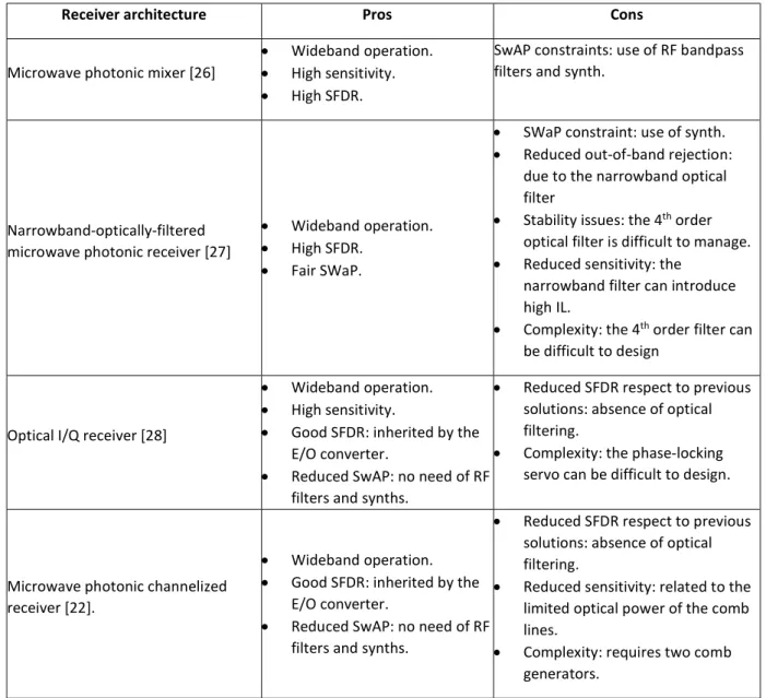
1.2.1. Microwave photonics receivers for Electronic Support Measures
Microwave photonics filtering and down-conversion techniques are being proposed in full-spectrum (0.5 – 40 GHz) RF receivers. In fact, photonic technology allows extremely large tunability
(in excess of 100GHz), and negligible bandwidth variation, resulting an attractive option for wideband operations with low SWaP and high performance [11].
In [26], a microwave photonic down-converter has been introduced. Using commercially available components, the architecture demonstrates photonic down-conversion at X-Band with an SFDR near 120 dB ∙ Hz2/3 outperforming conventional microwave mixers by at least 30 dB. On the other
hand, this simple but effective solution does not provide image-rejection capabilities, and bulky RF passband filters must be used to select the desired portion of the RF input spectrum before down-conversion, in order to avoid aliasing at IF. Moreover, the system requires a synthesizer as tunable electrical local oscillator (LO) to perform the scanning of the RF input, with considerable SWaP implications in the final footprint.
Compact, narrow band optical filters, with passband tunability of 1.9-5.4 GHz, can be used to select the down-converted input portion of RF spectrum, and thus perform the image rejection. In [27], a photonically-enabled receiver that filters and down-converts the RF spectrum in the optical domain, has been presented. An SFDR of 116 ∙ dBHz2/3 is measured. This scheme, on the one hand
avoids the use of RF bandpass filters but, on the other, requires a synthesizer (as LO) to achieve the tunability. Moreover, the exploited fourth-order tunable optical filter is rather complex to manage (and design) and shows limited out-of-band rejection (32 dB). In addition, the insertion loss (IL) introduced by the narrowband optical filter can reduce the final sensitivity of the receiver.
The critical task of precisely filtering the RF spectral portions in the optical domain can be simplified exploiting optical direct conversion techniques, i.e., in-phase/quadrature (I/Q) detection [28]. This technique exploits two CW lasers: one is used for the O/E conversion of the RF input signal, the other acts as optical local oscillator (LO) for the E/O down-conversion at baseband. Therefore, this scheme allows moving the filtering function at baseband, where simple low-pass electrical filters (LPFs) can be used after the optical-to-electrical conversion. It is worth noting that the optical direct conversion approach is instead immune to the issues of local oscillator self-mixing and RF to baseband feedthrough (high IF - RF and LO - RF port isolation), which affect the conventional direct conversion receivers [20]. Besides, the architecture requires a phase locking servo that stabilizes the phase fluctuation between the two CW lasers, in order to reduce the phase noise of the electrical signal generated after the O/E conversion.
In [22], a photonics-based channelization scheme has been proposed. It does not need complex narrowband tunable optical filtering, nor bulky RF bandpass filter banks and synthesizers. Nevertheless, these advantages are traded off with a more complex and less flexible setup, requiring
two coherent optical frequency comb generators to perform the channelization task. Moreover, the flatness response of the receiver in the whole operating bandwidth is related to the flatness of the generated optical comb lines, while the noise figure and sensitivity are related to the optical power of each comb line.
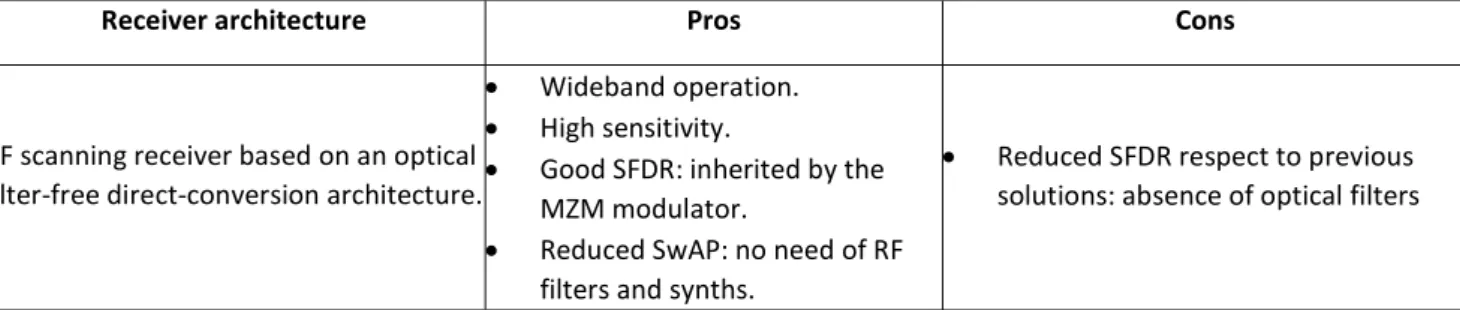
A detailed principle of operation and the pros and cons comparisons for these architectures are presented in Section 2.5.
The work presented in this thesis tries to push further the exploitation of photonic techniques in wideband RF receivers, in order to obtain a single stage, widely tunable architecture that avoids any bulky components as microwave filter banks, synthesizers, multiple crystal oscillators, switches, but also DC blocks and complex calibration circuitry, thus permitting a plain on-chip integration and the achievement of the key performance parameters required by the next generation multifunctional receivers (see table 1), at the same time.
Paragraph 1.1.2 states that a next-generation ESM receivers should be composed by a high probability-of-interception (POI) stage for immediate detection of the 0.5 – 40 GHz spectrum (i.e. a radar warning receiver - RWR - architecture), and a high performance tunable stage that satisfies the requirements of Table 1 with SWaP reduced as much as possible (Fig.1.5-A). As depicted in Fig.1.5-B, a photonics-based tunable receiver would replace the pure electronic counterpart, thus eliminating the SWaP constraints related to the multiple RF bandpass filters and local oscillators (LOs), exploited by the electronic solution to cover the 0.5 – 40 GHz operating bandwidth.
Fig.1.5. Scheme of principle of the (A) electronics- and (B) photonics-based next-generation 0.5 – 40 GHz Electronic Support Measures receiver proposals. RWR: radar warning receiver; POI: probability of interception;
SWaP: size, weight, and power; LO: local oscillator.
RWR Tunable receiver Processing High performance Low SWaP High POI Low SWaP Photonics-based RWR ~ LO Tunable receiver Processing High performance Low SWaP High POI Low SWaP
Main SWaP constraints
A) B)
Electronics-based
Chapter 2
Microwave photonics for RF systems
The present chapter provides a simple background for the rest of the dissertation. In particular, the attention is focused on the photonic devices techniques that have been used for the realization of the architectures reported in the next chapters.
As stated in Chapter 1, a microwave photonics system use the advantages of photonic technologies to provide functions in microwave systems that are very complex or even impossible to carry out directly in the RF domain. First, it performs an electrical-to-optical (E/O) conversion of the input electrical signal, then processes the signal in the optical domain, and finally realizes an optical-to-electrical (O/E) reconversion as output of the system (Fig.2.1).
Some of the most important functions that microwave photonics conveniently fulfills in the optical domain are wideband RF transport and distribution (e.g. antenna remotization or cable encumbrance reduction), time delay or phase shifting (e.g. beamforming), filtering, signals mixing (for up- and down-conversion), etc.
In the next sections the E/O and O/E conversion are taken into account.
2.1 Electrical-to-optical conversion
This section presents a brief explanation on the devices and techniques used for up-converting RF signal to optical frequencies (electrical-to-optical conversion), in order to exploit the advantages of the photonic technology.
The two optical components that take role in this process are:
the laser source, that generates the carrier (or carriers) at optical frequencies (around 1550 nm i.e. ≈193.69 THz). Usually, it is a semiconductor laser.
Fig.2.1. Scheme of principle of a microwave photonics system.
E/O Conversion Processing Optical
Electrical
in O/E ConversionElectrical
out the electro-optical modulator, that modulates the optical carrier by using the RF input signal. Usually, a Mach-Zehnder modulator.
They are detailed in the following. 2.1.1. The semiconductor laser
A laser is a device that emits light through a process of optical amplification based on the stimulated emission of electromagnetic radiation. A laser differs from other sources of light in that it emits light coherently. Spatial coherence allows a laser to be focused to a tight spot, enabling applications such as laser cutting and lithography. Lasers can also have high temporal coherence, which allows them to emit light with a very narrow spectrum, i.e., they can emit a single color of light. A laser oscillator consists of a gain medium, and an optical resonator (composed by a reflector and optical coupler) that provides optical feedback (Fig.2.2). The gain medium is a material with properties that allow it to amplify light by way of stimulated emission. Light of a specific wavelength that passes through the gain medium is amplified. The laser pumping energy is typically supplied as an electric current or as light at a different wavelength.
Among the various types of lasers present in the market and in laboratories (semiconductor-, solid-state-, fiber-based, etc.), the semiconductor lasers (based on semiconductor gain media) are the most important type of lasers. Their applications are extremely widespread, including areas as diverse as optical data transmission, optical data storage, metrology, spectroscopy, material processing, etc., due to their practicality, compactness, adequate performance, and cost. A wide range of wavelengths are accessible with different devices, covering much of the visible, near-infrared and mid-near-infrared spectral region. Most devices also allow for wavelength tuning, for example acting on the driving current that pumps the gain medium.
2.1.2. The Mach-Zehnder modulator
In the early optical communications era, the most common way for modulating an optical signal consisted in directly modulating the current driving the laser sources [29]. This approach presented mainly two drawbacks: first of all, the produced signal was often affected by an undesired frequency chirp and, secondly, the obtained dynamic range is usually not suitable for state-of-the-art microwave photonics applications [11]. Electro-optic modulators (EOMs), on the other hand, are fundamental devices in optical communications, since they allow to modulate light more efficiently than with direct modulation.
One of the most commonly employed EOMs is the Mach-Zehnder modulator (MZM), whose name is due to its structure, conceptually based on the Mach-Zehnder interferometer. This device employs one or more Pockels cells which can exhibit an efficient linear electro-optic effect, causing a variation of the medium’s refractive index which, in turn, changes the propagation velocity of light, thus influencing the signal’s phase [30]. Indeed, a MZM can be seen, as depicted in Fig.2.3, as an optical path equally split in two arms, with a phase modulator (PM) on each (or, in some cases, only on one) branch. The two paths then recombine again and, acting on the individual refractive index of each arm, the output signals exhibit an amplitude modulation.
The phase variation, introduced by the PM, can be expressed as a linear function of the applied voltage:
( ) = − (2.1.1)
where Vπ is the half-wave voltage, i.e. the minimum necessary voltage to obtain a π-shift of the
field phase in the PM.
Let us consider an optical field at the input of the MZM like:
( ) = ∙ (2.1.2)
Considering that there is a PM on each branch, and that they are driven by two voltages V1(t) and
V2(t), the optical field, after equal splitting, independent phase modulation on the two paths, and
equal coupling, can be written as: ( ) =
2 ∙
( )
+ ( ) (2.1.2)
Therefore, the amplitude response of the modulator is: ( ) = ( ) − ( )
2
( ) ( )
(2.1.3) The power response is obtained as the square absolute value of the amplitude response:
( ) = ( ) − ( )
2 (2.1.4)
with V(t) = V2(t) − V1(t). The amplitude and power response are reported in Fig.2.4 as a blue and a
red curve, respectively.
2.2 Optical-to-electrical conversion
After the processing in the optical domain (i.e. filtering, amplification, mixing with other RF signals, etc.), the RF input is reconverted to the electrical domain as output of the microwave photonics system. This process occurs as beating of the modulated optical signal at the photodiode.
2.2.1. The photodiode
The photodetector or photodiode (PD) is a fundamental device for receiving an optical signal. In general, it is a transducer, because it transforms in a current the photon flux impinging on it; more precisely, it produces at its output a current, called photocurrent, that is proportional to the optical input power.
The PD is based on the p-n junction, that is composed by a p-doped and a n-doped semiconductor region, between two electrodes, as shown in Fig. 2.5. This kind of PDs are referred to as p-i-n photodiodes, where "p" and "n" refer to the material different doping, whereas "i" stands for the middle "intrinsic" layer, which is created primarily to increase the bandwidth of the device (respect to a simple p-n structure).
The current intensity at the output of the PD can be expressed as:
( ) = ( ) (2.2.1)
The parameter R (responsivity) is measured in A∙W−1. Equation (2.2.1) shows the linear relation
between the photocurrent intensity and the optical power. For this reason, from this point on in this dissertation, we will consider the PD as simply as a block whose output is the square of the input electric field’s amplitude |E|, since P ∝ |E|2, thus
( ) =∝ | | ( ) (2.2.2)
2.2.2. Optical direct detection
The research and development in optical fiber communication systems started in the first half of the 1970s. Such systems used intensity modulation of semiconductor lasers (i.e. using a
Zehnder modulator biased in quadrature, Vπ/2), and the optical signal intensity transmitted through
an optical fiber was detected by a photodiode, which acted as a square-law detector (see Eq.2.2.2). In a direct detection receiver, its photo-detector only responds to changes in the receiving signal optical power, and cannot extract any phase or frequency information from the optical carrier. Therefore, direct detection is also called non-coherent detection [31]. This combination of the transmitter and the receiver is called the intensity modulation and direct detection (IMDD) scheme (Fig.2.6), which has been commonly employed in optical communication systems up to the present date. Such IMDD scheme has a great advantage that the receiver sensitivity is independent of the carrier phase and the state of polarization of the incoming signal, which are randomly fluctuating in real systems. On the other hand, they present lower performance in terms of dynamic range, noise figure, and sensitivity respect to coherent detection schemes (see Section 2.2.3).
Moreover, in IMDD systems, the optical domain filtering processing is not straightforward [16]. In fact, even though microwave photonics incoherent filters are stable and free from environmental fluctuations, they suffer several limitations: only real and positive values of the filter impulse response can be easily obtained (because optical intensity cannot be negative), the out-of-band rejection of the filter is limited, and the filter structures are bulky and difficult to integrate.
2.2.3. Optical coherent detection
With coherent receivers, we can restore full information on optical carriers, namely in-phase and quadrature components (or amplitude and phase) of the complex amplitude of the optical electric field and the state of polarization of the signal. In exchange for such advantages, coherent receivers are sensitive to the phase and state of polarization of the incoming signal. To cope with this problem, the configuration of coherent systems becomes much more complicated than that of IMDD systems [31].
Fig.2.7-A depicts the scheme of principle of a basic coherent heterodyne receiver.
Coherent detection therefore offers several key advantages compared to direct detection:
Fig.2.6. Scheme of principle of an intensity modulation and direct detection (IMDD) system. MZM: Mach-Zehnder modulator; PD: photodiode.
E/O Conversion Laser
RF
in MZMRF
out O/E Conversion PD Greatly improved receiver sensitivity. The shot-noise-limited receiver sensitivity could be achieved by injecting a sufficient optical local oscillator (LO) power into the receiver to combat against circuit noise. Moreover, when using balanced detectors with a high common mode noise rejection ratio (CMRR), signal-to-noise ratio (SNR) can be improved further.
Can extract amplitude, frequency, and phase information from an optical carrier, and consequently can achieve much higher capacity in the same bandwidth.
Cavity based optical filters, that act on the amplitude and phase of the optical electric field, can be exploited in microwave photonics filtering schemes in a straightforward fashion (see Section 2.5). In in-phase/quadrature (I/Q) schemes (Fig.2.7-B), also called homodyne or direct conversion architectures, optical domain filtering can be achieved by LO tuning without the use of an optical filter or demultiplexer [31].
It should also be noted that laser phase noise of the optical carrier and LO is an important impairment in coherent systems as it impacts the “phase coherence”. The “linewidth” parameter of a laser diode is directly related to its phase noise. In particular, the absolute linewidth of the laser is not important, but the relative linewidth of the two lasers (carrier and LO) must be small enough to drive coherent processes. A locking technique between the two lasers (i.e., optical
phase-Fig.2.7. Scheme of principle of a coherent (A) heterodyne and (B) homodyne (direct conversion) detection scheme. MZM: Mach-Zehnder modulator; PD: photodiode; LO: local oscillator; I/Q:
in-phase/quadrature. Balanced O/E Conversion I1(t) I2(t) I(t) LO Laser PD E/O Conversion Carrier Laser RFin MZM RFout I/Q O/E Conversion I1(t) I2(t) II(t) LO Laser Carrier Laser RFin MZM RFout E/O Conversion I1(t) I2(t) IQ(t) 90 °O pt ic al H yb rid
A)
B)
180° Couplerlocked loops, injection locking) can be introduced to improve the phase coherence of their electrical beating.
Figure 2.6-A shows the configuration of the coherent optical receiver. The fundamental concept behind coherent detection is to take the product of electric fields of the modulated optical carrier and the continuous-wave (CW) local oscillator (LO). Let the optical signal after the Mach-Zehnder modulator be
( ) = ( ) (2.2.3)
where As(t) is the complex amplitude and ωs the angular frequency. Similarly, the electric field of
LO at the receiver can be written as
( ) = ( ) (2.2.4)
where ALO is the constant complex amplitude and ωLO the angular frequency of LO. We note here
that the complex amplitudes As and ALO are related to the signal power Ps and the LO power PLO by
Ps = |As|2/2 and PLO = |ALO|2/2, respectively.
Balanced detection uses a 3-dB optical coupler that adds a 180◦ phase shift to either the signal field or the LO field between the two output ports (180°-coupler).
The output photocurrents are written as (details can be found in [31]) ( ) =
2 ( ) + + 2 ( ) + ( ) − ( ) (2.2.5)
( ) =
2 ( ) + − 2 ( ) + ( ) − ( )
(2.2.6) where ωIF is known as the intermediate frequency (IF) given by ωIF = |ωs − ωLO|, and θsig(t) and
θLO(t) are phases of the transmitted signal and LO, respectively. R is the responsivity of the
photodiode. PLO is always constant and θLO(t) includes only the phase noise that varies in time.
The balanced detector output is then given as
( ) = ( ) − ( ) = 2 ( ) + ( ) − ( ) (2.2.7) Balanced detection is usually introduced into the coherent receiver as a means to suppress the DC component Ps(t) + PLO and maximize the signal photocurrent.
Heterodyne detection (Fig.2.6-A) refers to the case that |ωIF| >> ωb/2, where ωb is the modulation
bandwidth of the optical carrier. In such a case, Eq. (2.2.7) shows that the electric field of the signal light is down-converted to the IF signal including the amplitude information √Ps(t) and the phase
information θsig(t).
Homodyne detection refers to the case that ωIF = 0. Preparing another LO, whose phase is shifted
signal light. This function is achieved by a 90° optical hybrid shown in Fig. 2.7-B. Using such 90° optical hybrid, output photocurrents from balanced photodetectors are then given as
( ) = ( ) − ( ) = ( ) ( ) − ( ) (2.2.8) ( ) = ( ) − ( ) = ( ) ( ) − ( ) (2.2.9) Using Eqs. (2.2.8) and (2.2.9), we can restore the complex amplitude as
( ) = ( ) + ( ) = ( ) ( ) − ( ) (2.2.10) Equation (2.2.10) shows that the electric field of the signal light is down-converted to the baseband in contrast to heterodyne detection.
2.3 Multi-frequency optical sources
This section briefly introduces and analyzes the most important techniques and technologies used for the generation of multi-frequency optical sources, and their exploitation for the generation and detection of RF signals with high precision and efficiency. All these solutions are largely adopted in the novel architectures proposed in this thesis.
2.3.1. The mode-locked laser
A mode-locked laser (MLL) is a pulsed laser that can be realized exploiting a lot of different methods. Regardless the particular adopted implementation, a MLL’s output signal is a periodic train of short pulses and, as a consequence, its frequency spectrum is discrete. This kind of lasers are called mode-locked because every line in the spectrum satisfies the phase-locking condition; in other words, the oscillations composing the pulsed signal are always in phase.
In principle, ordinary continuous-wave (CW) lasers are composed by a resonator (e.g. an etalon, like a Fabry-Perot filter) with one (or both) partially reflective facet. Inside this resonant cavity, a gain medium is present. When the latter is pumped, its spontaneous emission gives rise to a plenty of longitudinal sinusoidal oscillations, the modes of the cavity. Because of the internal interference, the only "possible" modes are the ones whose wavelength satisfies the following relation:
=
where L is the cavity length. Taking into account the cavity losses, the majority of these modes vanishes, and the only surviving modes correspond to wavelengths for which the gain is higher than the losses. In Fig. 2.8, the blue curve represents the gain spectrum, whereas the green straight line the cavity losses, which are assumed to keep constant not only in frequency, but also all over the cavity length. The modes are represented by different shades of grey: the lightest one are outside the emission spectrum of the active medium, and therefore they can never be generated; on the other hand, the other deeper-grey modes can exist, although they all vanish but the central one. Indeed, this latter is the only mode for which the gain equals the losses, so that the mode can be sustained in the cavity, whereas the others are to be cancelled by the attenuation. Eventually, the laser output is a sine wave at optical frequency corresponding to the angular frequency ωM, or to
the wavelength λM, according to the relation
= 2 (2.3.2)
where c is the speed of light. So the gain bandwidth of the active medium has to be large enough or, alternatively, modes have to be spaced closely enough, to get a spectrum composed by several lines.
The operation of the mode-locked laser can be understood as follows: in the absence of an electrical mode-locking input signal, the laser will operate in multiple longitudinal cavity modes with random phases between them. When a strong modulation of the gain from an external RF source is applied with frequency equal to the longitudinal cavity mode spacing, or a harmonic thereof, the previously randomly-fluctuating modes become phase-locked to each other. Each optical mode of
Fig.2.8. Scheme of cavity modes generation. The blue curve represents the gain, whereas the green one is the attenuation. The light-grey arrows are the rejected modes, and the
deep-grey arrows are the suppressed modes. The black arrow in the middle is the only sustained mode.
the laser acquires sidebands due to the electrical modulation signal. When the frequency of the modulation signal equals the cavity mode spacing, the modulation sidebands mutually injection-lock the neighboring optical modes, causing all of the modes to establish a fixed phase relation between them. In this condition, the phase-locked modes cause the time-domain output to be a train of short pulses at a repetition rate equal to the mode-locking frequency. The width of the pulses is determined by the number of modes locked. Sub-picosecond pulses can be produced with mode-locked lasers, which requires that the locked optical modes span more than 1000 GHz of optical bandwidth.
Therefore, since a MLL emits a periodic train of ultrashort identical pulses, it has a spectrum composed by several modes, spaced by the pulse repetition frequency, and its spectrum envelope is the same as the shape of a single pulse spectrum. This entails that the pulse duration τp is
approximately the inverse of the spectrum width. In Fig.2.9 the ideal spectrum of a MLL is depicted. As an example, the spectrum shape is a Gaussian curve, meaning that the pulse shape itself is Gaussian. Moreover, the pulse repetition rate is in relation with the cavity dimension. By comparing Fig.2.8 with Fig.2.9, it is easy to understand that the gain bandwidth of the active medium has to be large enough or, alternatively, modes have to be spaced closely enough, to get a spectrum composed by several lines.
Fig.2.9. Schematic example of a MLL frequency spectrum. Tr represents the pulse
Nowadays, the MLL are solid-state devices that can be realized with semiconductor technologies, with the possibility of integration, or in glass fiber.
2.3.2. Cavity-less optical frequency comb generators
Optical frequency combs have been gaining lot of interest in the photonic field, as they are useful in many applications, such as microwave photonics [24], metrology [32], optical communications [33], etc.
In some SWaP constrained photonics-based receivers, combs with tunable wavelength and reconfigurable line spacing (of the order of few GHz or less) are highly desirable [20], while maintaining reduced footprint. In these cases, cavity-enhanced comb architectures (e.g. mode-locked lasers), i.e., resonant structures whose physical dimensions determine the wavelength and spacing of the comb [34], can be not suitable, while simple cavity-less schemes can reveal most appropriate. As depicted in Fig.2.10, they consist in a single continuous wave (CW) laser (at wavelength νoc) followed by a cascade of intensity (i.e. Mach-Zehnder modulators) and phase
modulators (IM-PM cascade) driven by tunable RF sinus waves at frequency fm [20,35]. The obtained
comb repetition rate corresponds to the RF driving the modulators. In these schemes, the maximum number of generated comb lines primarily depends on the phase modulation index, i.e., the amplitude of the signal driving the phase modulator normalized to its halfwave voltage Vπ.
Therefore, increasing the number of comb lines requires larger driving signals. Considering the practical case of phase modulators driven at their maximum accepted voltage, doubling the number of comb lines actually requires doubling the number of phase modulators [20]. When many comb
Fig.2.10. Scheme of principle of an IM-PM comb generator. MZM: Mach-Zehnder modulator; PM: Phase modulator; CW: continuous wave.
f
m~
Optical CW input Optical Comb output
MZM PM
λ
@
f
mν
OCλ
lines are needed, the number of required phase modulators makes this approach bulky, expensive and power hungry, vanishing the straightforwardness of the architecture with respect to the cavity-enhanced counterpart.
A flat frequency comb is generally desired, the interesting theoretical work of Torres-Company et al. [20], which proposed a novel way of understanding the spectral flatness achieved in previous schemes. When a flat-topped pulse is subjected to a strong, periodic, quadratically varying temporal phase, it undergoes time-to-frequency mapping, resulting in a flat comb due to the shape being similar to the time domain intensity of the input waveform.
Therefore, a convenient approach to generate flat-topped pulses is to use an intensity modulator driven with a sinusoid with an amplitude V = Vπ/2 of the modulator and a DC bias corresponding to
a phase shift of ϕdc = −π/2 [35]. The role of the intensity modulator is to produce a train of
pseudo-square pulses when biased appropriately. This way, the pulses carve the CW laser only where the chirping provided by the phase modulation is almost linear, thus equalizing the spectrum. Again, the optical bandwidth of the comb is proportional to the modulation index introduced by the phase modulator.
2.4 Injection locking of semiconductor lasers
In this section, optical injection locking of semiconductor lasers is introduced as a convenient approach to single optical frequency comb (OFC) mode filtering and amplification without any additional narrowband optical filter or electronic control.
Optical injection locking is a way of synchronizing one (or several) free-running laser oscillators to a reference one [36], in order to exploit them for low phase-noise optical heterodyning.
Optical heterodyning techniques for microwave signal generation, distribution, and processing have attracted much interest in antenna-remoting, phased-array antenna beamforming, optical-microwave communication links, frequency converting fiber optic links, radio astronomy, and coherent communication systems [37]. They also find applications in spectroscopy, atomic physics, metrology, and interferometry. A stable optical heterodyne signal generator would benefit many RF systems. Such system would be the optical equivalent of the traditional electronic frequency synthesizers employed in RF electronic systems, which would allow the use of optical heterodyne techniques in the processing of RF, microwave, and millimeter-wave signals using optical components instead of electronic components. This would allow fuller advantage to be taken of the inherently large RF bandwidth of optical fiber and optical components such as couplers, isolators, switches, attenuators, delay-lines, and optical amplifiers.
The absolute linewidth of the laser is not important, but the relative linewidth of the two lasers must be small enough to drive coherent processes. Generation of RF optical heterodyne signals with low RF phase noise is non-trivial. Typically, an electronic phase-locked-loop (PLL) is required to keep the optical heterodyne beat locked to an external reference frequency. Without a feedback loop, the instantaneous linewidth of the millimeter-wave beat frequency generated by optical heterodyning is on the order of the individual laser linewidths, which are typically 1 MHz – 10 MHz if DFB semiconductor lasers are used. This linewidth is three to six orders of magnitude larger than what is achievable by frequency multiplication of an electronic reference into the microwave frequency range. Also, slow frequency drifts of the absolute frequencies of the lasers ranging from several MHz to more than 1 GHz are superimposed on the instantaneous quantum-limited linewidth [38]. Because of the difficulty of realizing a wideband PLL for microwave through millimeter-wave optical heterodyne generation, this technique has remained mostly a laboratory curiosity and is not widely employed in RF photonic systems applications.
Laboratory experiments have demonstrated injection-locking of independent laser diodes to a master laser diode that is injection-modulated to produce individual continuous-wave (CW) narrow linewidth lasers could be obtained at any wavelength of the comb spectrum by selecting and amplifying a single comb mode of an OFC without any additional high-finesse Fabry-Perot cavity [38]. However, producing a single-longitudinal-mode CW laser output from a single OFC line is challenging because of the limitations of conventional optical filters and the extremely weak power of each comb mode among the millions of frequency modes with the spacing of several hundred MHz.
A solution can be optical injection locking, which offers a convenient approach to single comb mode filtering and amplification without electronic control. Even the amplitude noise from the master laser can be suppressed under certain conditions. The main task of this method is to get large amplification of a single comb line while suppressing the side modes as much as possible. The Photonic Synthesizer architecture demonstrated the amplification of selected modes from OFCs by means of spectral-mode filtering and femtosecond laser injection-locking [37]. High phase stability is achieved in this optical heterodyning system by combining the outputs of two independently tunable "slave" lasers that are injection-locked to different optical modes of a "master" optical comb generated by and OFC generator of a mode-locked laser (see Fig.2.11). The slave lasers act as tunable narrow-band optical filters that pick out two modes of the reference frequency comb to produce a heterodyne output signal with very low phase noise.
For the Photonic Synthesizer, the phase of the detected RF heterodyne beat is determined essentially by the relative phases between the selected optical modes. There is also residual phase noise due to spontaneous emission, but the analysis in [38] indicates that it is generally neglectable. When optically-injection-locked, the phase fluctuations of the slave lasers follow the phase fluctuations of the master mode-locked laser. Due to the high correlation of the phase fluctuations of the individual modes of the mode-locked laser, a high-quality microwave to millimeter-wave signal is produced from the heterodyne beat of the two injection-locked CW DFB lasers.
Fig.2.11 illustrates the principle of operation for the Photonic Synthesizer. When the optical pulse train from the mode-locked laser is injected into the CW DFB laser, the DFB laser can be phase-locked to that mode of the mode-phase-locked laser, provided the injection-locking bandwidth of the DFB is smaller than the mode spacing of optical comb. The injection-locking bandwidth (or locking range) of the slave laser depends on the power Pi of the injected mode which is tuned close to the
free-running frequency of the slave laser. Fig.2.12 shows the locking range (dark curves) as a function of the injection power Pi to the DFB slave laser power P , Pi / P, called optical injection ratio (dB). When
the frequency detuning value, i.e. the frequency difference between the injected mode and the free-running DFB, is inside the area defined by these two curves, the slave laser phase can lock to the master laser phase.
Other modes outside the locking range will introduce phase modulation on the DFB laser. As the locking bandwidth of the DFB laser is decreased, these phase modulations become smaller, i.e. the other modes are filtered out by the slave laser. However, if the DFB laser locking bandwidth is too
Fig.2.11. Scheme of principle of the Photonic Synthesizer presented in [PhotSynt]. MLL: mode-locked laser; DFB: distributed feedback semiconductor laser; PD: photodiode; ν: optical frequency; f: electrical frequency.
small, locking the slave laser to the desired mode becomes more difficult, particularly if either the mode-locked laser comb fluctuates in the frequency domain, or if the DFB laser frequency fluctuates. The optimum locking bandwidth is determined from the experiments as a compromise between the stability of injection locking and the sideband suppression.
In the Photonic Synthesizer setup, the mode-locked laser is split and simultaneously injected into two DFB lasers as shown in Fig.2.11. When the free-running frequency of DFB1 is adjusted to the
frequency of the ith mode of the mode-locked laser (i.e. the ith mode frequency is inside the locking
range of DFB1), and DFB2 is adjusted to the frequency of the jth mode of the mode-locked laser, the
DFB lasers will be injection-locked to ith and jth modes of mode-locked laser, respectively. Thus, the
frequency difference between DFB1 and DFB2 is precisely set to the frequency difference of ith and
jth modes of the mode-locked laser, which is an integral multiple of its cavity length (see Eq.2.3.1).
The phases of the slave lasers also assume the same phases as the ith and jth modes of mode-locked
laser.
2.5 Microwave photonics broadband architectures
Photonic techniques are being proposed in RF receivers to implement the filtering and down-conversion tasks over wide frequency bands. In fact, microwave-photonic techniques allow extremely large tunability (in excess of 100GHz), and negligible bandwidth variation, which make the use of photonics an attractive option for microwave operations up to 100GHz with a low SWaP and high performance fashion [11].
Fig.2.12. Locking range as a function of the injection power to DFB slave laser output power ratio, Pi/P (dB). When the frequency detuning value is inside the area defined by two dark curves, the slave laser phase can lock to
In these solutions, the broadband RF signal is first electrical-to-optical (E/O) converted by modulating a continuous wave (CW) laser in a Mach-Zehnder electro-optic modulator (MZM) (Fig.2.13), then it is processed in the optical domain, and finally it is optical-to-electrical (O/E) down-converted to intermediate frequency (IF), or baseband, by means of the beating at a photodiode (PD).
This section describes the state of the art of photonic solutions for wideband receiving applications, highlighting the advantages respect to the pure electronic counterparts.
In [26], a microwave photonic down-converting mixer has been introduced (Fig.2.14). The system split a CW laser in two optical carriers and modulates the RF signal and local oscillator (LO) onto them. The modulation sidebands are filtered in the optical regime by using tunable optical filters with tens of GHz of bandwidth. This step is critical to the performance. By removing lower sidebands and harmonics before optical-to electrical conversion, the spurs are greatly reduced. The SFDR of the microwave photonic link with photonic down-conversion was compared with the SFDR from a conventional microwave mixer. In every spur measurement, the photonic mixer outperformed the conventional microwave mixer by at least 30 dB. As empirically demonstrated in [26], mixing in the optical regime provided significantly reduced spurious signals over state-of-the-art electronic mixers
Fig.2.13. Scheme of principle of a generic photonics-based RF receiver.
Fig.2.14. Scheme of principle of the microwave photonic down-converting mixer presented in [26]. The architecture requires an RF bandpass filter before the E/O conversion of the RF input. It also requires a
synthesizer as tunable electrical LO.
CW Laser
E/O
ConversionProcessing
OpticalRF
inO/E
ConversionIF
outCW Laser
E/O
ConversionFilter
Tunable wideband opticalRF
inO/E
Balanced conversionIF
outE/O
ConversionLO
inFilter
Tunable wideband optical RF filterwhile maintaining operation over wider instantaneous bandwidths. The balanced optical-to-electrical conversion also rejected common mode noise such as Relative Intensity Noise (due to the CW laser) and Amplified Spontaneous Emission beat noise (due to optical amplifiers). Using commercially available components, the architecture demonstrates photonic down-conversion at X-Band with an SFDR near 120 dB ∙ Hz2/3. On the other hand, this simple but effective solution does
not provide image-rejection capabilities, i.e. bulky RF passband filters must be used to select the desired portion of the RF input spectrum before down-conversion, in order to avoid aliasing at IF. Moreover, the system requires a synthesizer as tunable electrical local oscillator to perform the scanning of the RF input, with considerable SWaP implications in the final footprint.
High order, narrow band optical filters, with passband tunability of 1.9-5.4 GHz, can be used to select the down-converted input portion of RF spectrum, and thus perform the image rejection. In [27], a photonically-enabled receiver has been presented that filters and down-converts the RF spectrum in the optical domain (Fig.2.15). An SFDR of 116 ∙ dBHz2/3 is measured, enhanced by the
optical domain filtering respect to the performance of the E/O conversion. However, the scheme generates the tunable optical LO directly from the continuous wave (CW) laser, by modulating it with a widely tunable RF synthesizer, with significant SWaP implications. Moreover, the exploited fourth-order tunable optical filter is rather complex to manage (and design) and shows limited out-of-band rejection (32 dB). In addition, the insertion loss (IL) introduced by the narrowband optical filter can reduce the final sensitivity of the receiver.
The critical task of precisely filtering the RF spectral portions in the optical domain can be simplified exploiting optical direct conversion techniques, i.e., in-phase/quadrature (I/Q) detection [28]. This technique eploits two CW lasers: one is used for the O/E conversion of the RF input signal,
Fig.2.15. Scheme of principle of the narrowband-optically-filtered microwave photonic receiver presented in [27]. The architecture does not require RF bandpass filters. It requires a synthesizer as tunable electrical LO.