UNIVERSITÀ DEGLI STUDI DI CATANIA
Dottorato di Ricerca in SCIENZE CHIMICHE
Ciclo XXIX
Surface engineering of oxide systems
for energy and molecular electronics applications
Stefania Vitale
Tesi di dottorato di ricerca
Gennaio 2017
Tutor: Prof. A. Licciardello
Coordinatore: Prof. S. Sortino
A chi ha sempre creduto in me,
a volte facendolo anche per me.
“It is our responsibility as scientists, knowing the great progress and great
value of a satisfactory philosophy of ignorance, the great progress that is the
fruit of freedom of thought, to proclaim the value of this freedom, to teach
how doubt is not to be feared but welcomed and discussed, and to demand
this freedom as our duty to all coming generations.”
Richard Feynman, “The Pleasure of Finding Things Out”
“Science is not everything, but science is very beautiful.”
1
Riassunto
La modifica di superfici mediante deposizione di film sottili di molecole funzionali costituisce un interessante approccio tecnologico per il miglioramento di varie proprietà superficiali di un materiale. Sono virtualmente infinite le possibilità di progettazione di superfici funzionali con proprietà speciali impartite dai sistemi molecolari utilizzati, poiché virtualmente infinite sono le molecole che possono essere sintetizzate e le proprietà che in esse possono essere introdotte (ottiche, elettriche, strutturali, ecc…). Quando tali molecole vengono integrate sulla superficie di un materiale avente anch’esso
per se proprietà speciali, il risultato è un nuovo sistema allo stato solido avente
dimensioni nanometriche e caratteristiche derivate dalle “fusione” di quelle delle molecole ancorate e quelle della superficie. Per ottenere un’efficace “combinazione” molecola-superficie, tuttavia, l’approccio sperimentale utilizzato per la preparazione del substrato e per l’integrazione del sistema molecolare sono di importanza cruciale per l’ottenimento di un buon risultato. In questo contesto le metodologie impiegate devono essere messe a punto in maniera mirata, per garantire l’ancoraggio stabile di specifiche molecole su specifiche superfici.
Il presente lavoro di tesi è stato dedicato alla modifica di superfici mediante ancoraggio di sistemi molecolari funzionali per future applicazioni nell’ambito dell’elettronica molecolare e dell’energia. L’obiettivo principale è stato la messa a punto di una metodologia sperimentale che consentisse un ancoraggio stabile delle specie molecolari desiderate su superfici di ossidi di interesse tecnologico, quali gli ossidi trasparenti e (semi)conduttori (TCOs). Per fare ciò è stato sfruttato un approccio basato sulla chimica dello zirconio fosfato-fosfonato, che consiste in un priming superficiale preliminare (ZP-priming) attraverso la deposizione di uno strato sottilissimo (monolayer) di fosfato di zirconio direttamente alla superficie di ossido. Tale strato, come dimostrato dalle evidenze sperimentali riportate, funge da robusta “piattaforma” per il successivo ancoraggio di sistemi molecolari recanti un gruppo fosfonico, su ossidi di diversa morfologia e natura chimica.
La strategia di priming ZP è stata applicata con successo al trattamento di substrati nanostrutturati, di spessore micrometrico (5-10 μm) di TiO2 ed SnO2.
2
L’ottenimento di un priming uniforme è stato confermato attraverso l’acquisizione di profili di profondità (depth profiling) mediante spettrometria di massa di ioni secondari ToF-SIMS. ZP-TiO2 e ZP-SnO2 sono stati in seguito
utilizzati come substrati per la preparazione di elettrodi fotoattivi, che possono trovare utilizzo in celle solari colorante-sensibilizzate (dye-sensitized cells). È stato dimostrato che il trattamento ZP produce un’ottima piattaforma di ancoraggio per le molecole di colorante fotoattivo RuP (un terpiridil-triazin complesso di rutenio (II) funzionalizzato con un gruppo fosfonico), mentre misure di depth profiling ToF-SIMS hanno permesso di monitorare la diffusione del colorante nel layer di ossido nanostrutturato, mostrando che tutto lo strato micrometrico viene sensibilizzato con il colorante. Inoltre, da misure di spettroscopia UV-Vis è emerso che il trattamento preliminare ZP introduce alcuni vantaggi, ovvero un incremento della stabilità del legame molecola fotoattiva-ossido, nonché un maggiore uptake di molecole di colorante. Da misure fotoelettrochimiche (caratteristiche JV sotto irraggiamento) si è visto inoltre che la presenza dello strato di fosfato di zirconio all’interfaccia fra ossido e molecole di colorante non influisce negativamente sul processo di iniezione di carica dal colorante all’ossido (alla base del funzionamento delle celle solari a colorante), e di conseguenza la funzionalità dell’elettrodo è del tutto paragonabile a quella di un classico elettrodo colorante-sensibilizzato “non ZP”.
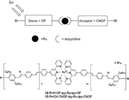
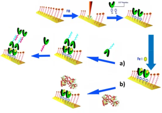
L’utilizzo di ZP-TCOs è stato inoltre esteso alla preparazione di fili molecolari conduttivi, questi ultimi “assemblati” depositando complessi metallo-polipiridinici direttamente alla superficie di ossido, attraverso successive reazioni di coordinazione. In una prima fase, è stata preparata una superficie funzionalizzata con unità terpiridiniche, mediante ancoraggio del sistema molecolare ditopico PPTP (acido (4-(2,2’: 6’-2’’-terpiridin-4-ile) benzen-fosfonico) su ZP-FTO; le unità terpiridiniche libere alla superficie sono state in seguito utilizzate come sito di ancoraggio per le molecole bifunzionali di RuDT2 (Ru(II)-bis[4′,4′′′′-(1,4-fenilene)bis(2,2′:6′,2′′-terpiridina)]), attraverso
reazione di coordinazione metallica da parte di ferro (II) delle una terpiridine in superficie con una delle due unità terpiridiniche della molecola RuDT2.
Attraverso cicli iterativi di reazioni di coordinazione, sono stati preparati fili molecolari contenenti diverse unità Fe-RuDT2, e l’avvenuta crescita è stata
confermata mediante misure ToF-SIMS e spettroscopia UV-Vis. La conduzione elettrica lungo i fili molecolari è stata studiata mediante
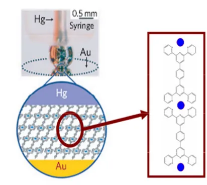
liquid-metal EGaIn junction, e i dati raccolti mostrano una buona conduzione della
3 oro. La possibilità di integrare sistemi elettricamente conduttivi di complessi metallo-polipiridina su superfici di ossidi conduttori e trasparenti, attraverso la piattaforma ZP-PPTP, permette di prendere in considerazione applicazioni nell’ambito dell’elettronica molecolare, con possibile estensione all’elettronica “fotoresponsiva”, considerato che le unità metallo-terpiridina sono notoriamente dei centri fotoattivi.
5
Table of contents
Preface ... 7
1. Introduction and state of the art ... 11
1.1. Progress in photovoltaics: the molecular approach for solar energy conversion ... 12
1.1.1. Dye-sensitized solar cells (DSSCs) ... 13
1.1.1.1. The photoanode: molecular approach for dye-sensitization of TiO2 electrodes……… ... 16
1.1.2. Dye-sensitized Photoelectrosynthesis Cells (DSPECs) for photoinduced water splitting ... 21
1.1.2.1. SnO2 as alternative photoanode material for DSPECs ... 29
1.1.3. Current challenges of Dye-sensitized Cells ... 30
1.2. Nanoscale molecular electronics ... 33
1.2.1. Charge transport mechanism in molecular systems ... 38
1.2.2. Polypyridine-based metal complexes ... 40
1.2.3. Liquid metal junctions in molecular electronics ... 45
1.3. Surface modification using zirconium phosphate-phosphonate chemistry .... 48
2. Results and discussion ... 53
2.1. Introduction ... 54
2.2. Anchoring of photoactive molecular systems on ZP-primed nanostructured oxide surfaces ... 56
2.2.1. ZP priming of nanostructured TiO2 surfaces ... 57
2.2.2. Diffusion behaviour of Zr(IV) in nanostructured TiO2 substrates ... 63
2.2.3. Effect of ZP layer on dye-to-oxide charge injection ... 71
2.2.4. Anchoring stability of phosphonate-derivatised organic molecules on ZP-primed TiO2 surfaces ... 73
2.2.5. Assembly of photoactive molecules on nanostructured ZP-primed TiO2 ... 79
6
2.2.5.2. ToF-SIMS and spectroscopic characterisation ... 82
2.2.5.3. Photoelectrochemical measurements on dye-sensitized ZP-TiO2 ... 86
2.2.6. Assembly of photoactive molecules on nanostructured ZP-primed SnO2 ... 91
2.2.7. Conclusions ... 97
2.3. Molecular wires on ZP-primed FTO ... 99
2.3.1. Synthetic approach for the stepwise growth of RuDT2 wires ... 101
2.3.1.1. ToF-SIMS investigation ... 105
2.3.1.2. UV-Vis characterisation ... 107
2.3.1.3. EGaIn electrical measurements ... 110
2.3.2. Conclusions ... 117
3. Conclusions and perspectives ... 119
4. Appendix: Materials and Methods... 121
7
Preface
Surface engineering has become an indispensable tool for the improvement of a number of properties of solid surfaces. Nowadays modification techniques such as thin film deposition, (photo- and electron-)lithography, laser and plasma treatments are largely employed to tailor various surface properties and lead to new functional materials being used in different fields, such as advanced electronics, optoelectronics, optics, energy harvesting and medical devices.[1]
A particular interesting and relatively simple modification technique consists in the chemical deposition of thin molecular layers at the materials’ surface. This approach has been extensively studied in the last decades, both for fundamental studies on intermolecular interaction at solid interfaces (but also generic intermolecular interactions) and functional surfaces development.[2, 3] The main advantages of molecular surface engineering are: i) specific functional molecular systems can be purposely synthesised to tailor specific properties to the desired surface ii) the flexibility and the relatively ease and low-cost manufacturing of organic synthesis could provide virtually infinite variety of molecular systems having diverse properties (optical, electrical, tribological, etc..), iii) the extremely small size of molecules (< 1 nm) allows for the preparation of nanometre-scale systems through a “bottom-up” approach. The latter point fulfils, among others, the requirements of the miniaturisation trend in the development of modern devices and allows to tackle all the physical and technical limits faced by established surface technologies such as photolithography.[4]
In molecular engineering of solid surfaces the choice of the molecular systems if crucial for the achievement of the desired properties. This choice, of course, is strongly affected also by the nature of the surface to be modified so that, globally, the achievement of the particular desired goal, in terms of system properties, must take into account both the counterparts (molecular system and solid substrate) as well as their interaction. In other words, parallel to the choice of specific molecular systems to be anchored, the selection of the substrate to be functionalised is not of least importance. Specific materials have specific chemical composition, structures and surface properties, which must be taken into account when thinking about a successful “molecule-surface” match for a well-defined application.
8
In the last two decades, significant scientific and technological interest has been addressed to oxide materials, especially metal oxides. A good summary of the reasons which justify this widespread interest can be found in a review by Diebold et al.:[5] “Among metal oxides are superconductors and the best
insulators; some oxides are inert enough to act as corrosion protection layers, whereas others are chemically active as catalysts. Some of the most interesting magnetic, optical and electronic properties are found within this class of materials.”
Particular interest is focused on transparent conductive oxides (TCOs). The importance of those materials arises from their good electrical properties coupled with the transparency in the visible region.[6]
As a consequence of the above mentioned appealing properties, the scientific interest in molecular engineering of technologically-relevant oxide surfaces expanded rapidly in the last years, and the research on this topic led to functionalised-surface (“engineered”) oxides that can actually find application in various fields such as electronics,[7-11] optoelectronics,[12, 13] catalysis[14] and sensors.[15, 16]
One of the most interesting field of application of oxide molecular surface engineering deals with the development and realisation of molecular devices which are able to perform light-induced functions, the so called Photochemical Molecular Devices (PMD).[17] In such devices the molecular system is chosen to fulfil specific light-induced functions (like photo-induced electron transfer), and it is subsequently integrated on a convenient solid substrate, which would be both a “support” for the immobilisation of the molecular system and, most important, an active component of the final device. Such a system can find application in a number of technological areas, such as those involving light harvesting, elaboration of optical signal information, energy production and biological applications.
In this framework, a remarkable example of photoactive devices which are able to photochemically convert the energy of the solar radiation in electric energy (or energy fuels) are the so-called Dye Sensitized Cells, such as Dye Sensitized Solar Cells (DSSCs) and Dye-Sensitized Photoelectrochemical Cells (DSPECs). The working principle of these devices is based on sunlight absorption by a photoactive dye molecule anchored onto the surface of a nanostructured, transparent, micrometres-thick semiconductor oxide, followed by injection of an electron from the excited state of the dye to the conduction band of the semiconductor.
9 Another interesting example of application of surface-integrated photoactive molecules consists in the preparation of nanometric solid state photoresponsive molecular junctions,[18] consisting in a thin film of light-sensitive molecules densely packed between two electrodes. Light-induced excitation of this molecular layer leads to charge dissociation and subsequent collection at the electrodes, making this system suitable for working as an optoelectronic switch or an optically responsive memory.
Apart from the choice of a molecular system bearing specific chemical and electronic structures capaple to be practically exploited for “actual” devices realisation, the development of all the above mentioned photoactive devices relies critically on a proper integration of the functional molecules onto the solid substrate. The molecular film has to be firmly bound to the surface through a stable interface, which has to allow for a robust anchoring of the molecules and, at the same time, for the “communication” between substrate and molecular system. Usually this goal is achieved by exploiting the chemical affinity of some specific functional group (which the molecular system would be equipped with) to the surface of a substrate. A general and easy approach involves the anchoring by chemisorption of the molecules onto the surface from liquid solutions, by simply immersion of the solid substrate in a low-concentration (usually millimolar) solution of the molecular system. As example of application of this approach, Self-assembled monolayers (SAMs) and Langmuir-Bodgett films are certainly amongst the most famous.[19] These solution-based methods, however, require a careful planning of each reaction step, with special concern on the reaction conditions (solvents, temperature, reaction time,…) and all the experimental parameters involved.
Parallel to the development of reliable and reproducible methods for the preparation and modification of functional molecular surfaces, specialised analytical techniques are necessary for the precise characterisation of the surface properties (such as chemical composition, structure, optical and electric properties, etc..), in order to elucidate the variety of physico-chemical phenomena down to the single molecule level and their effect on the macroscopic properties of the modified surface.
Among the available surface analysis techniques, time-of-flight secondary ions mass spectrometry (ToF-SIMS) can be considered one of the most powerful, because it allows for the chemical characterisation of the surfaces with very high sensitivity and good spatial resolution, allowing not only the detection and bi- or three- dimensional mapping of all elements (including hydrogen) but
10
also providing a large amount of molecular information on the species present at the surface and, with some limitations, along the depth of molecular films. This thesis work is focused on the modification of oxide surfaces via anchoring of functional molecular systems, for applications in solar energy conversion and in molecular electronics. In particular, a functionalisation strategy based on the zirconium phosphate/phosphonate chemistry has been investigated, with the aim of developing an effective experimental strategy for achieving a robust and reproducible anchoring of functional molecules on oxide surfaces of different chemical nature (TiO2, SnO2, fluorine-doped tin oxide) and
morphology (flat and nanostructured). Some specific preparation methodologies have been developed and optimised for the assembly of different special photoactive molecules on technologically-interesting oxide substrates. The obtained systems were extensively characterised by ToF-SIMS technique, jointly to UV-Vis spectroscopy. “Functional” characterisation was also carried out by means of photoelectrochemical measurements and liquid-metal junction technique.
The thesis is divided in different sections. The first, “Introduction and state
of the art”, is an overview of the state of art and acts as an “introduction” to
the experimental work performed. It gives some background information about the context of application of some molecular-functionalised oxides in the field of dye-sensitised cells for solar energy conversion and nanoscale molecular electronics. The second section “Results and discussion” deals with the description and discussion of the experimental results, and it is divided in two subsections. In the first one, results are presented on the functionalisation of nanostructured, transparent, semiconducting oxide surfaces by means of photoactive dye molecules, whilst in the second section the assembly of conductive molecular wires on a transparent conductive oxide is reported, along with some results on their electrical properties. Finally, some general Conclusions and perspectives are outlined. In order to render more fluid the presentation and discussion of the experimental results, many experimental details are reported in a separate appendix “Material and Methods”.
11
12
1.1.
Progress in photovoltaics: the molecular approach
for solar energy conversion
Progressive depletion of fossil fuels imposes to look for new energy sources for the (always increasing) needs of industrial, commercial and everyday-life activities. The supply of renewable and environmentally sustainable energy has become one of the major task of modern society, in order to limit fossil fuels depletion and also the environmental effects of their employment (pollution, global warming, etc..).
Among all the renewable energy technologies proposed over the years, photovoltaic technology based on solar energy exploitation is considered as the most promising one.
Solar radiation amounts to 3.8 million EJ/year (3,8·1024), which is approximately 10,000 times more than current world energy needs[20]. The idea of converting part of this huge amount of energy in an exploitable form has led to the development of solar photovoltaic cells, devices that convert solar energy directly to electric energy. The “conventional” first and second generation solar cells are based on semiconducting materials, mainly silicon, but also other semiconductors such as CdTe and CIGS. These cells are inorganic solid-state junction devices, which can convert sunlight radiation in electricity with 15-20% of efficiency. Despite their good performances, their production requires high manufacturing and maintenance costs, which prevents limits their actual widespread diffusion. Meanwhile, other alternatives are being explored such as molecular-based solar cells, namely heterojunction organic photovoltaic cells, polymeric thin films-based solar cells and nanocrystalline semiconductor-based ones. Similarly to the processes involved in the natural photosynthesis, all the above mentioned systems operate in virtue of a charge-separation achieved by electron injection from a molecular photoinduced excited state to the conduction band of a semiconductor material. Due to this molecular-based charge separation, those kind of cells generally show worse efficiency in sunlight conversion if compared to silicon-based cells (in which light absorption leads directly to the generation of free conduction band electrons and valence band holes; see Figure 1 for a schematic representation), but this is – at least in principle - compensated by considerably cheaper manufacturing costs. The technological interest on such
molecular-13 based cells is also given by the possibility of specific market applications, like low temperature processing on plastic substrate and subsequent ease of integration into established printing lines.[21]
Figure 1: Schematic comparison between light absorption by molecular materials (left) and silicon-based materials (right). (Adapted from ref. [21]).
In this framework, one of the currently most attractive systems, for both scientists and engineers, is represented by the so-called Dye-Sensitized Solar Cells, which are going to be presented in the next paragraph.
1.1.1.
Dye-sensitized solar cells (DSSCs)
A dye-sensitized-cell exploits a nanostructured, large-bandgap and transparent semiconductor oxide, in combination with a photosensitizer, usually a chromophore molecule.
The general configuration of a dye-sensitized solar cell and its operating principle are sketched in Figure 2.
The cell is normally built using the following components:
1. A photoanode, consisting on a mesoporous semiconducting oxide layer (usually TiO2 in anatase phase), deposited onto a glass slide covered
with a thin film of transparent conducting oxide (usually FTO, fluorine-doped tin oxide), and then sensitized with a monolayer of photoactive
14
dye molecules covalently attached to the surface of the mesoporous oxide;
2. a cathode, prepared with a glass slide covered with a catalyst (usually platinum);
3. an electrolytic medium, which is in direct contact with both electrodes, and contains a redox agent (usually the redox couple I-/I3-, dissolved in
an organic solvent, like acetonitrile).
Figure 2: Scheme of a DSSC.
The process of solar energy conversion occurs through four main steps (listed below).[22] It starts with the absorption of a photon from the chromophore, which induces an electron transition from the fundamental state to an excited state (1). This process is followed by the injection of an electron from the excited state to the conduction band of the nanostructured oxide (2). Then, the oxidized dye molecule is reduced (and so regenerated) by the reducing agent present in the electrolytic solution (provided that the HOMO of the dye molecule is low enough to accept electron donation from the electrolyte) (3). The circuit is closed when the reducing agent that has been oxidized is again restored at the cathode, by receiving an electron through an external circuit (4).
15 1) Dye + hν → Dye*
2) Dye* + TiO2 → Dye+ + (e-, TiO2)
3) 2Dye+ + 3I- → 2Dye + I3
-4) I3- + 2e- → 3I
-The performance of this kind of cell is evaluated on the basis of two parameters, efficiency (η) and fill factor (FF):
100%
where JSC is the short circuit current density (mA cm-2), VOC is the open-circuit
voltage (V), Pin is the incident light power, Jmax and Vmax correspond to the
values of current density and voltage, respectively, at the maximum power output given in the cell J-V curve (see Figure 3 for a graphic representation of the efficiency-related parameters).
Figure 3: typical J-V curve for a DSSCs, where all the efficiency-related parameters are labeled.
The prototype of the first dye-sensitized solar cell was realised by O’Regan and Grätzel and the outcome results published in 1991.[23] In this paper, a photovoltaic device was described, which was based on a 10um-thick layer of optically transparent TiO2 film of small nanoparticles, coated with a monolayer of a charge-transfer dye to sensitize the titania film for light
16
harvesting. This cell showed an overall light-to-electric energy conversion higher that 7% in simulated solar light and 12% in daylight. The great performances of this “pioneering” photovoltaic device, combined with the low-cost and easy manufacturing largely justify the huge interest of both researchers and industries on the improvement of such a technology for solar energy conversion.
Following the leading work of O’Regan and Grätzel, a large number of dye-sensitized cells have been reported afterwards, with modified specific components (dyes, oxide electrodes, electrolyte, …) but with the same “backbone”, remained mostly unaltered until present days.
1.1.1.1.
The photoanode: molecular approach for
dye-sensitization of TiO
2electrodes
Among all the components of a dye-sensitised cell, the most crucial role on the cell functionality is played by the photoanode. Here are located the chromophore agents able to absorb the sunlight and here charge separation takes place after solar light absorption, with electron injection from the dye to the oxide conduction band.
In order to be used in a dye-sensitised cell photoanode, a nanostructured semiconductor oxide must meet different requirements, in particular:
1. a large band gap, allowing for transparency in the visible region of the solar emission spectrum;
2. large surface area;
3. long chemical and thermal stability under irradiation; 4. highly efficient electron collection and injection.
For DSSCs, the oxide material which fulfils all the above mentioned requirements, and has been chosen as substrate of election for photoanode preparation, is titanium dioxide. It occurs naturally in three phases: anatase, rutile and brookite. Anatase TiO2 is the best suited phase for application in
DSSCs, having a 3.2 eV bandgap, higher than the 3.0 eV of rutile (the latter being, however, the most thermodynamically stable phase), lower electron recombination rate [24] and it allows for the adsorption of a greater amount of dye molecules, due to the higher specific surface area. [25]
17 In addition, titanium dioxide is abundantly available, non-toxic and has cheap manufacturing costs. Despite many other oxide materials have been (and are still being) tested, such as ZnO [26-28], SnO2[29, 30] and Nb2O5[31, 32],
titanium dioxide still remains the one which gives the best cell performances in terms of efficiency.
For the preparation of the photoanode a mesoporous layer of oxide is needed, having a thickness of several micrometers (~ 10). The reason for the utilisation of electrodes with such a morphology lies on the large surface area available for the accommodation of the photosensitiser molecules. Given that the dye molecules actually make the DSSCs working, the more molecules we have at the photoanode surface, the more light can be absorbed and converted to electric energy. Furthermore, an oxide thickness in the order of 10 μm gives the right balance between TiO2 electrode transparency in the visible region of
the spectrum, efficient light harvesting and a pore size compatible with electron- as well as electrolyte solution diffusion.[23, 33-35]
The most common approach for the preparation of the mesoporous TiO2 layer
consists in spreading a mixed polymeric-TiO2 nanoparticles paste over the FTO
substrate, through either “doctor blade” technique or screen printing (Figure 4), following a 30 minutes sinterisation treatment at 450° C. Typical titania nanoparticles diameter ranges between 10 and 30 nm, and they are usually prepared by sol-gel synthesis or hydrolysis of TiCl4.[36] Apart from
nanoparticle-based electrodes, also other kind of nanostructure are under investigation for the constant improvement of photoanodes performances, such as nanotubes, nanorods, nanosheets, etc…[37]
Figure 4: schematic representation of a) "doctor blade" deposition technique and b) screen printing. (Adapted from ref. [38]).
18
In parallel to the choice of the best suitable substrate to prepare the electrode with, serious attention must be paid on the selection of the dye to be used for sensitisation. The light-absorber molecule has to meet itself several requirements in order to give the desired functionality to the cell: [39]
1. it should absorb as much as possible the visible light up to a threshold of 920 nm (this limit has been extracted from thermodynamic calculations on the light conversion efficiency at different light wavelength)[40, 41];
2. it should be able to inject electron (upon photoexcitation) into the electrode conduction band with ideally unitary quantum yield, provided that the energy level of the excited state of the dye (i.e. LUMO of the molecule) matches with the edge of the conduction band;
3. It should have functional groups allowing for chemical anchoring onto the oxide surface (e.g. –COOH, –PO3H2,…);
4. its redox potential should be high enough to allow for the regeneration of the dye via reduction from the redox electrolyte;
5. it must be photostable, and electrochemical as well as thermal stability are also required.
Given the above mentioned requirements, during years of research several different photosensitizer dye have been synthesised on purpose, including a number of chemical compounds such as transition metal complexes, phtalocyanines, porphyrins and metal-free organic dyes.[42]
Among all those systems, Ru(II)-polypiridyl metal complexes emerged as excellent candidates for being exploited as photosensitiser in dye-sensitised cells.
Polypyridine-based ruthenium complexes are amongst the most interesting photoactive molecular systems, in virtue of a number of outstanding (photo)physico-chemical properties. They show strong absorption in the visible region (which could be also extended to near IR region through a suitable choice of lateral substituents of the polypyridyl units), strong electronic coupling between the MLCT excited state and the semiconductor conduction band (which allows for fast exctited state deactivation via dye-to-semiconductor electron injection, happening in a timescale of femtoseconds), and great chemical stability.[43, 44]
The first time when a solar-to-electric energy conversion efficiency of 10% was reached dates back to 1993, when Nazeeruddin and coworkers[45] published data on a dye-sensitized cell built with a
cis-(SCN)2bis(2,2’-19 bypyridyl-4,4’-dicarboxylate) ruthenium(II) photosensitizer, coded as N3 (Figure 5 a)). Subsequently, in a study of the effect of the proton content in N3 dye, it turned out that the double protonated form, indicated as N719 (Figure 5b) exhibited enhanced power conversion efficiency and a redox potential shifted to more negative potential in solution (condition that favourably increase the Jsc achievable).[46] In an attempt to continuously improve the efficiency of dye-sensitized cells, an extension of the absorption spectrum of the sensitizer to the IR region would be highly desirable; in this framework Gratzel and co-workers synthesised the N749 dye, also known as “black dye” (Figure 5c). With this molecule as photosensitizer, their cell showed a broad red-shift in absorption and a spectrum of IPCE (incident photon-to-current efficiency) over the entire visible range up to 920 nm in the near-IR, as well as an overall conversion efficiency of 10.4 %.[47]
Figure 5: Chemical structures of ruthenium photosensitisers a) N3, b) N719, c) black dye.
From their first use as photosensitizer, N3, N719 and the black dye became reference points for the development of more efficient dyes, and they are today still used as a “starting” point for the design of new sensitizer bearing different ligands and substituents with respect to the “originals”, in order to conveniently improve their optical and photophysical properties.
In order for the charge separation phenomena (whose proper functioning of the cell relies on) to properly occur, the availability of the “best” sensitizer, meeting all the previously mentioned conditions, is a necessary condition
20
although not sufficient per se. Among all the required conditions [25] one of the most crucial to be fulfilled is the good quality of the binding between the chromophore and the oxide surface. Given that the sensitizer ensures the solar light absorption, it has to be strongly bound to the surface in order to ensure the best functionality of the cell as well as long term durability. Moreover, the good “communication” must be guaranteed between chromophore molecules and semiconductor oxide, to allow for the dye-to-oxide charge injection. As a consequence of those issues, the obvious outcome is that the photoanode must be designed with utmost care, with a special focus on the dye-sensitization procedure of the nanostructured titania layer, in order to obtain the optimal performances and best device efficiencies achievable.
As previously mentioned, the sensitization procedure is usually carried out by attaching the photoactive system on the TiO2 surface through a chemical bond
between the oxide and a dye molecule carrying a functional group being able to bind to the surface.
The typical functionality currently in use is the carboxylic group, due to the large availability of natural and synthetic dyes, commercial accessibility and relatively good stability.[42] However, the carboxylic group-oxide bond is labile in certain conditions, for example in alkaline solutions,[48] and can be easily broken even with simple rinsing with organic solvents,[49] A number of other functional groups have been investigated, such as silane and sulphonate,[42] but currently one of the most valid alternative to carboxylic functionality appears to be given by the phosphonic groups. Since the first study reported by Péchy et al,[50] phosphonic units have been proven to bind to TiO2 surfaces stronger than carboxylic groups, and they show greater
stability after exposure to both organic solvents and aqueous media, as well as in a wide range of pH.[51-54] The different binding strength and stability can be ascribed to a different reactivity of the two functional groups, caused by the different number of coordination sites that they have, respectively two for the carboxylic unit and three for the phosphonic one. This leads to different anchoring structure in the two cases, that is mono- and bidentate for carboxylate linkages and mono-, bi- and tridentate for phosphonate linkages (Figure 6).[53]
21
Figure 6: Surface bonding schemes for carboxylate (left) and phosphonate (right) linkages. (Adapted from ref. [53])
Although the stronger binding capability on TiO2 surfaces and the more stable
anchoring in comparison to the carboxylate one, it is known that phosphonate ester linkage on metal oxides (as well as the carboxylate) is susceptible to hydrolysis when exposed to aqueous media. Moreover, although in a smaller extent respect to carboxylated photoactive systems, desorption processes of the phosphonate dye in the common operating condition of the DSSC can occur and they negatively affect the performances of the cell and its lifetime. Later in the text (see paragraph 1.1.3), possible solutions will be discussed for the minimisation of desorption of photoactive molecules from the oxide surface.
1.1.2.
Dye-sensitized
Photoelectrosynthesis
Cells
(DSPECs) for photoinduced water splitting
As implicit in the very definition of photovoltaic solar cells, a DSSC can supply electric energy only in presence of the sunlight. Giving the fact that the sun is an “intermittent” source, in perspective of the ideal total replacement of energy production from fossil fuels, energy storage systems are required in order to provide power at night.[55]
A number of storage schemes have been proposed, or are in use,[56] but the only practical approach at the required scale is “Artificial Photosynthesis” with “solar fuels” as the product.
Solar fuels, according to Bolton definition, are reduced chemical substances produced by endergonic photochemical reaction, which are able to release the stored chemical energy upon reaction with oxygen.[57] Giving that their production would exploit only cheap and easily available “reagents” (i.e. water, CO2 and sunlight), solar fuels hold great promise as a permanent,
22
environmentally friendly, long-term and globally-available renewable energy source.
An appealing approach to solar fuels generation by artificial photosynthesis is based on Dye-Sensitized Photoelectrosynthesis Cells (DSPECs) for photoinduced water splitting. These devices mimic the electrodes configuration used in DSSCs, but with a different goal: achieving a photoinduced reaction (rather than the generation of photocurrent), which leads to the production of oxygen and hydrogen, with the latter being a high energy solar fuel.
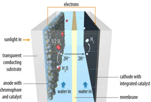
The configuration of a dye-sensitized photoelectrosynthesis cell is sketched in Figure 7.
Figure 7: Scheme of a dye-sensitized photoelectrosynthesis cell for photoinduced water splitting (Graphic by Yan Liang, copyright L2Molecule.com).
The design of a DSPEC shares some component with a dye-sensitized solar cell, but also important different features are present. The configuration of these cells consists in the following crucial elements:
23 1. Photoanode: as in a DSSC, it is constituted by a nanostructured, transparent and semiconducting oxide sensitized with a photoactive molecular system, being able to capture the sunlight;
2. Water Oxidation Catalyst (WOC): it can be a molecular system or an inorganic compounds which uses oxidising equivalents to oxidise water to oxygen gas and H+ ions; it must be assembled on the photoanode, together with the molecular dye;
3. Reduction Catalyst: it is the counterpart of the WOC, and it uses reducing equivalents to store energy in the form of reduced material (i.e. hydrogen); for photoinduced water splitting usually platinum is used (in the form of cathode), in virtue of its low overpotential (activation energy) and rapid turnover for proton reduction to hydrogen gas.
Water oxidation and H+ reduction are achieved in two different compartments of the cell, kept separated by a proton exchange membrane (PEM), which allows for the diffusion of H+ ions and charge balance.
The overall water splitting reaction (equation 3) takes place in virtue of two half reactions (equations 1 and 2):
2 → + 4 + 4 (1) 4 + 4 → 2 (2)
2 → 2 + (ΔG0 = +4,92 eV) (3)
This reaction is quite an energy demanding process: it request at least an input energy corresponding to 1,23 V (vs NHE at pH 0)[58] in order to take place. However, the application of a consistent overpotential is demanded in order to actually carry out the reaction due to the complexity of the process, which involves several intermediates for an overall four electron oxidation per molecule of water.
For a proper understanding of how each component of a DSPEC contributes to the overall water splitting process, a scheme of its working mechanism is presented in Figure 8.
24
Figure 8: Scheme of the water splitting process occurring in a DSPEC (top, adapted from [59]) and molecular reactions involved (bottom; Cat: water oxidation catalyst).
The process starts with the absorption of a photon from the molecular dye. This step is followed by an electron injection from the photoinduced excited state of the dye to the conduction band of the nanostructured oxide anode, and after the electron is transported to the counter electrode. Subsequently, the fundamental state of the dye is restored by electron transfer from the WOC and the latter uses the oxidising equivalent to oxidise H2O to oxygen gas and H+. Finally the
generated protons diffuse through the PEM and migrate toward the reduction catalyst-equipped cathode, where they are reduced to hydrogen gas.
The first example of dye-sensitized photoelectrosynthesis cell dates back to 1999, when Meyer and co-workers published preliminary results on hydrogen production using a photoelectrosynthesis cell based on the absorption of a bis-ruthenium polypyridyl complex on nanocrystalline TiO2 substrate.[60] The
Ru-complex employed was actually the dpp-bridged molecular assembly [(4,4’-(CO2H)2bpy)(4,4’-Me2bpy)Rua(dpp)Rub(tpy)(OH2)]4+ (Figure 9), which
25 and a ruthenium monoxo-terpyridyl part, whose structure is analogous to that of well-known redox Ru and Os complexes that show catalytic two-electron oxidation.[61]
Figure 9: Structure of compound [(4,4’-(CO2H)2bpy)(4,4’-Me2bpy)Rua(dpp)Rub(tpy)(OH2)]4+.
(Adapted from ref. [60])
The authors used a two-compartment cell, one compartment with the sensitized TiO2 electrode immersed in 2-propanol solution and one containing a Pt
counter electrode. Upon irradiation with visible light, production of H2 was
observed, with parallel oxidation of 2-propanol to acetone.
Similarly to the case of DSSCs, many studies on dye-sensitized photoelectrochemical cells have been carried out employing different chromophores, semiconductors oxide and oxidation catalyst, but the “skeleton” of the cell remains almost unchanged.
Ruthenium polypyridyl complexes are still the dyes of election for the photoanode preparation, in virtue of all the favorable photophysical and photochemical properties already mentioned previously (see paragraph 1.1.1.1).
Concerning the water oxidation catalyst, various possibilities have been explored. One of the most notorious example of material that has been used as WOC is given by nanoparticles of semiconductor oxides, most successful being IrO2 nanoparticles. Due to its low electrochemical overpotential for
water oxidation,[62, 63] IrO2 (nanoparticulate or colloidal) has been widely
studied as water oxidation catalyst by itself.[64, 65] In combination with a molecular light absorber such as Ru(bpy)3,[66, 67] oxygen evolution takes
26
being the slow electron transfer from Ir(IV) to oxidised Ru(III), which result in poor catalytic efficiency and low turnover frequencies.[68]
Another class of molecular compounds that can be used for catalytic water splitting includes first-row transition metal complexes, whose chemical structure is tailored for mimicking that of the greatest water oxidation catalyst existing in nature, the oxygen evolving complex (OEC) of Photosystem II (PS II). This OEC is one of the main protein complex responsible for the light-induced oxygenic photosynthesis in plants, trees, algae, etc… Since the discovery of the existence of an Mn4 cluster (Figure 10a) within the OEC of
PSII,[69-71] several bioinspired tetramanganese complexes have been synthesised and tested for water splitting reaction, unfortunately showing poor catalytical activity.[72-74] Beside tetramanganese compounds, solid state cobalt cubane oxoclusters have also given promising results as WOCs, as Nocera and co-workers first reported.[75, 76] Subsequently several studies have been carried out on a particular cobalt cubane, namely [Co4(μ-O)4
(μ-CH3COO)4(C5H5N)4] (Co4O4-H, Figure 10b), using Ru(bpy)3 as
photosensitiser.[77-79] The results of photoelectrochemical measurements conducted in buffer solution, using persulfate as sacrificial agent, showed promising photochemical quantum yield for water splitting. However, the overall efficiency of the reaction relies critically on the experimental conditions adopted (e.g. catalyst concentration, pH, influence of the sacrificial agent itself on the catalytic activity, photoinduced degradation of the sensitiser ,…), and furthermore self-oxidation of the organic ligand on the WOC contribute as well to the poor durability of the catalytic system over the time.[80]
Figure 10: X-ray structures of a) Mn4CaO5 cluster in PS II (reprinted with permission from ref.
[81], copyright 2011 Nature Publishing Group) and b) cubane Co4O4-H (reprinted with permission
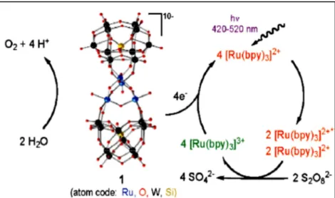
27 The issue of catalyst self-oxidation is overcome in the case of another class of molecular systems showing water splitting catalytic activity, namely polyoxometalates compounds (POMs). POMs are totally inorganic, polyanionic oxo-clusters of early transition metals (V, Mo, W, Nb, Ta) bound to a variety of other metals via oxo-bridges. The transition metals of POMs are normally in their highest oxidation state, and this is the reason of their great stability in strong oxidising conditions.[82] Among the various POMs tested for their perspective utilisation as WOCs, the [Ru4(μ-O)4(μ-OH)2(H2O)4
(γ-SiW10O36)2]10- (Ru4POM) emerged as one of the most promising catalyst for
water splitting.[83, 84] Its structure is reported in Figure 11. The photodriven water splitting activity tested in solution[83, 85] produced very promising overall performances, with high turnover numbers (up to 500) and turnover frequencies of ~ 0,60 s-1, and a 100 times increment in reaction rate with
respect to the experiment carried out without Ru4POM. A reaction mechanism
was proposed for the role of Ru4POM in water splitting, in a system containing
Ru(bpy)3 as photosensitizer and persulfate as sacrificial agent (see Figure 12 for
reaction scheme):[85] four photoexcited Ru(II)(bpy)3* give electron-transfer
reaction towards persulfate anions (which are reduced to sulfate), and the resulting four Ru(III)(bpy)3 are then reduced by the Ru4POM, the latter taking
this four electrons from the oxidation of water. In later works by Orlandi and Toma [86, 87] Ru4POM has also been studied as photocatalyst in
heterogeneous phase, and it was demonstrated that its “oxygenic” activity is maintained in solid-state electrodes.
Figure 11: Structure of Ru4POM (red: oxygen; grey: silicon; orange: ruthenium; light blue:
tungsten). Reprinted with permission from ref.[80], copyright 2012 The Royal Society of Chemistry.
28
Figure 12: Reaction mechanism for photoinduced water splitting in solution, using Ru4POM as
catalyser, Ru(bpy)3 as sensitiser and persulfate as sacrificial agent. Reprinted with permission from
ref. [85], copyright 2009 American Chemical Society.
It must be underlined that the perfect match of photosensitiser and water oxidation catalyst that one can test in a “solution benchmark” has to be always studied as well in heterogeneous phase (i.e. on a solid electrode), given that the ultimate purpose is the development of a solid-state solar device. The transfer of all the above mentioned molecular components on a solid surface is not a trivial matter, because the molecular anchoring of dye and WOC at the surface must be carried in a way thatensures good “communication” between each component and functionality of the electrode and, at the same time, ensures long term durability of the cell.
As for DSSCs, nanostructured titanium dioxide in anatase phase has been the first-choice substrate for the realisation of electrodes for dye-sensitized photoelectrochemical cells. However, despite its unquestionable success as photoanode in DSSCs, other type of semiconductor electrodes are currently being explored for applications in DSPECs, mostly because the electronic structure of TiO2 does not fit perfectly the ideal energetic requirements
29
1.1.2.1.
SnO
2as alternative photoanode material for
DSPECs
Nanostructured SnO2 electrodes are recurring candidates for the replacement of
TiO2 electrodes. Tin dioxide is a n-type and wide band gap (~ 3.8 eV)
semiconductor[29]. With respect to titanium dioxide, the conduction band of SnO2 is more positive (about +0.5 V), and this makes tin oxide a better electron
acceptor.[30] A comparative scheme for the electronic structure of TiO2 and
SnO2 is presented in Figure 13, with respect to the redox potential of H2O and
CO2 (the “fuels” for a DSPEC).
Figure 13: Electronic levels diagram comparing TiO2 and SnO2.(Adapted from ref. [88])
Tin dioxide substrates have been largely studied for applications in DSSCs[29-31, 89, 90], and the above mentioned energetic characteristic make it appealing also for application in realisation of DSPECs photoanodes. However, several drawbacks need to be overcome when using SnO2 photoelectrodes. The most
critical one is the significant slow regeneration of the dye by reaction with the electrolyte, caused by the competitive back-electron transfer reaction from the oxide to the redox electrolyte, whose rate is about three orders of magnitude faster than in the case of TiO2[91]. This is probably caused by the presence of
low-energy surface trap states on SnO2 [92]. A widely exploited approach to
limit this unwanted recombination phenomena is that of coating the nanostructured oxide electrode with a thin layer of high bandgap oxide, in
30
order to passivate it and lower (ideally block) the rate of undesired electron interception. Significant enhancement of the cell performances have been reported for dye-sensitized solar cells where the photoanode was covered with a layer of passivating-oxides such as Al2O3 (Figure 14)[93] or MgO[94]. Very
satisfying results were obtained also for DSPECs with SnO2 photoanodes[95]
covered with Al2O3 and TiO2 passivation oxides, deposited by ALD technique.
Figure 14: Proposed diagram for electron recombination phenomena in a DSSC with N719-sensitized SnO2 photoanode without (left) and with (right) Al2O3 passivation layer. Reprinted with
permission from ref. [93], copyright 2010 American Chemical Society.
1.1.3.
Current challenges of Dye-sensitized Cells
In dye-sensitized devices for solar energy conversion (both DSPECs and DSSCs) molecular systems play the most important roles and account for most of the cell work, because they absorb light, transfer electrons and provide the sites for catalysis.[55]
The major role played by molecules in the light-to-electric energy conversion and in the water splitting process is a big point in favour of dye-sensitized devices, because the current chemists’ abilities to synthesise molecular dyes and catalyst having specific optical properties and specific electronic structure allow for targeted modifications and improvements of the cell design and functionality. At the same time, however, the predominance of molecular reactions comes out with several drawbacks. Interfacial and intramolecular electron transfer dynamics are the most important factors to cite, because they
31 rely on the electronic structure of the employed molecules and determine the actual cell performances.
A scheme of the processes occurring at the interface of a dye-sensitized device (valid for both DSSC photoanode and DSPEC one) is presented in Figure 15.[96] In the normal operating conditions of a dye-sensitized cell, besides the molecular reactions that allows for the solar energy conversion (i.e. charge injection to the oxide conduction band from the excited state of the dye(1), electron collection at the electrode (2) and dye regeneration (3)), several competitive reactions take place, namely luminescence/non-radiative decay (4), electron recombination (5) and electron interception (6).
Figure 15: approximate energy diagram of a dye sensitized cell. Reprinted with permission from ref. [96], copyright 2008 The Royal Society of Chemistry.
The key for improving the solar cell performances is that of designing every single component as well as their “combination” in order to minimise reactions 4, 5 and 6 (i.e., ideally, they should be suppressed, or at least must happen in timescales much longer of those of the other desired reactions). Reaction 4 (luminescence/non-radiative decay) relies on the electronic structure, so in its respect the choice of the photoactive system must be done very carefully. On the other hand, reactions 5 and 6 (recombination and interception respectively) take place because of a “back-electron transfer” pathway between either the dye molecule or the redox electrolyte (or both of them). A possible strategy to minimise these reactions relies on the nanostructured electrode passivation,
32
which implies the realisation of an “interruption of communication” between the electrode and the “outside environment”. This approach, developed by covering the surface with a large bandgap insulating material has been broadly investigated, with good results and great improvement of the cell performances.[91, 97-99]
Another crucial point concerns the chemical linkage of the molecular dye/catalyst on the nanostructured oxide electrode, which should be strong enough to provide long term stability of the molecular binding and must be suitable for providing good “electronic communication” between chromophore/catalyst and the photoanode. Unfortunately, in the normal operating condition of DSSCs and DSPECs, dye-desorption phenomena occur, causing photoanode degradation and, as a consequence, severe cell efficiency losses.
Current research is exploring several approaches for minimising photoanodes degradation phenomena, the most promising being i) the use of co-adsorbed amphiphilic sensitizer and long alkyl-chain phosphonic acids,[100] and ii) chromophore binding stabilization via post-sensitizazion deposition of ALD coatings.[101, 102]
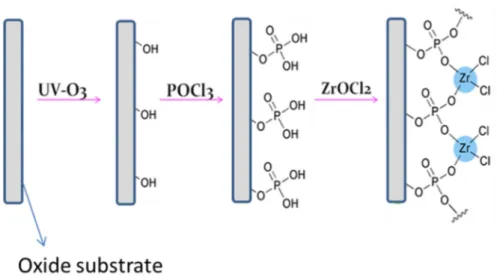
Another possible approach to enhance the stability of the dye-substrate linkage consists in creating an anchoring platform between the oxide surface and the photoactive molecular system. In our research group we developed a methodology that permits to create such platform on oxide surfaces, based on zirconium phosphate-phosphonate chemistry, and we refer to it as
ZP-priming.[103, 104] This surface treatment method is based on the well-known
chemical stability and robustness of ZP solids, and it consists in a stepwise procedure that leads to the deposition of a zirconium phosphate monolayer at the oxide surface, which can act as an actual anchoring platform for molecular systems bearing a phosphonic functional group. In the next paragraphs a more detailed description will be presented of zirconium phosphate-phosphonate systems and their use in surface modification.
33
1.2.
Nanoscale molecular electronics
During the last decades the miniaturisation trend of silicon-based electronics predicted by the Moore’s law[105] had to face the technological limits of its practical accomplishment. The main limitation consists in the “top-down” approach, which exploits preparation techniques, such as photolithography, for the realisation of patterned circuits. These approaches allow for a minimum lateral dimension in the order of hundreds of nanometres, due to the limits imposed by the wavelength of light (the magnitude needed to be in agreement with the prediction of Moore’s law should be towards the nanometre scale). Among the most valuable approaches to obtain a system of a few nanometres size, the “bottom-up” approach has the merits that it is based on the use of functional molecules as “building blocks”, which are assembled together in larger arrays. The creation of functional circuits starting from single molecular component is referred to as “molecular-scale electronics”, and its relevance is not limited to the fulfilment of the technological needs for traditional electronic devices miniaturisation, but it also provides a precious platform for studying the properties of materials at the nanoscale level.
Presently, the realisation of practically useful molecular electronic devices relies critically on the preparation techniques used to bind and assemble the functional molecules on the solid supports. Already in 1959 the physicist Richard Feynman foresaw the possibility of preparing extremely small electronic devices, during the ever since famous lecture entitled “There’s
plenty of room at the bottom”;[106] however at that time the scientific
knowledge was not yet ready to bring this visionary idea to life. But more than 10 years later the first proofs of the feasibility of Feyman’s idea started to show up. In this framework, between the 70’s and 80’s the pioneering work of Kuhn, Mann, Sagiv and Polymeropoulos provided the earliest data about charge transport through molecular systems.[107, 108] The measurements were carried-out on thin films of saturated, long-chain fatty acids deposited on the substrate with the first effective self-assembly technique, where the molecular systems were chemically bound onto the substrate surface through molecular bond formation, and not simply by physisorption via dispersion forces. This achievement subsequently opened the way to the development of molecular surface modification via Self-assembled Monolayer (SAM) technique.
34
The possibility of chemically binding, and so integrating, functional molecules on solid surfaces, spontaneously and in ordered structures, significantly promoted the studies on molecular electronics, leading to a widespread interest in the use of single molecules as components for the construction of functional circuits.
It also provided a powerful driving force for the development of experimental platforms capable of characterising the surface properties and probing electric physical phenomena (such as charge transport) at the molecular level.
The concept of using single molecules as functional electronic components implies that an electrical signal must pass in and out of the molecule, via contact-coupled electrodes; so in order to actually measure the electrical characteristics of the system, a molecular junction needs to be build, i.e. a contact between the single molecule and a second electrode must be realised. Several techniques are available for obtaining a molecular junction, but all of them have in common the same “basic” structure, given by the configuration metal-molecule-metal (sometimes indicated also as metal-insulator-metal). One of the milestones in this framework has come with the advent of Scanning Tunnelling Microscopy (STM) technique,[109] which gave the possibility to investigate both topography and electrical properties of the surfaces of molecular materials at the single-molecule level; other techniques include mechanically controllable break junctions (MCBJs),[110-112] electromigration breakdown[113, 114] and electrochemical deposition junctions.[115, 116] It should be pointed out that, from an experimental point of view, the realisation of single-molecule junction is technologically challenging and not easy to implement in large-scale production systems, thus limiting the practical applicability in real devices.[8] On the other hand, more robust and easier to prepare systems are those made by ordered (self)assemblies of a large number of functional molecules packed between two electrodes to allow for large-area electric measurement, the so called ensemble molecular junctions.[117] Among the systems most widely exploited for the fabrication of these kind of junction, self-assembled monolayers (SAMs) play a major role, due to their thermodynamic stability and easy-processing method (Figure 16). The simple immersion of the substrate in a solution of a suitable molecule (bearing a head-group able to chemically anchor onto the substrate) can lead to the formation of highly ordered and densely packed molecular thin films at the material surface (for a review on this topic see reference [118]).
35
Figure 16: Schematic diagram of SAMs preparation; a) schematic representation of molecular structure needed for SAM formation; b) immersion of the substrate in SAM-forming molecules solution, leading to ordered SAM film at the surface.
By means of ensemble molecular junctions, the electrical behaviour of several molecules has been studied, such as simple alkyl hydrocarbons as well as conjugated molecules.[119-122] An interesting case of study, which has given promising results for future practical applications, is given by conductive molecular wires (the wording being similar to that of more “classic” conductive wires of domestic electric systems). This term designate a large variety of 1D molecular systems of nanometric size (5-100 nm), usually built by (self)assembly of organic conjugated molecules, chemically bound to the surface of a conductive substrate (e.g. metals, oxides, …), which acts as electrode. By similarity with macroscopic electrical conductive wires, the concept of molecular wires is based on intramolecular electron transfer, and the current flow through the junction, where molecular wires connect the electrodes, depends on the energy gap between the Fermi levels of the electrodes and the frontier energy levels of the molecules within the wire (usually HOMO or LUMO).[123] The first studies on conductive molecular wires in second half of the nineties identified polyphenylene-based chains and carbon nanotubes as potential backbones for current-carrying molecular electronics,[124] and molecular wires of the two classes were intensively studied from both theoretical and experimental point of view.[110, 112, 125-130] Particular focus has been given later to polyphenylene-based wires; because of their small size (with respect to carbon nanotubes), they have high current densities which, combined with the well-established knowledge of their chemistry and synthetic flexibility, create a perfect match between “electrical” functionality and ease of preparation.[124] Given the above mentioned
36
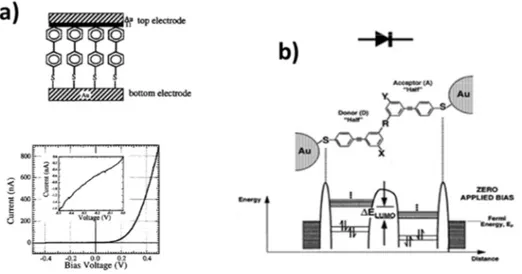
favourable conditions, a large number of studies were carried out and prototypical nanoscale electronic components such as molecular rectifiers and switches were realised, whose two examples, resulting from the word of Zhou[112] and Ellenbogen,[124] are presented in Figure 17.
Figure 17: a) Molecular rectification demonstrated by Zhou et al.; b) Polyphenylene-based
molecular rectifying diode switch, with scheme of predicted electron orbital energy levels. (Adapted from ref.[124]).
In order to improve the current flow through molecular wires, a well-known approach consists in the incorporation of redox-active sites within the organic backbone,[131, 132] especially metallic centres. As demonstrated by several studies,[133-136] in a (poly)metallic complex based wire the presence of metal redox sites provides low-lying, easy-to-reach, energy states, which promote the electron transfer rate through the wire.
The synthetic strategies used to assemble a polymetallic molecular wire can be roughly divided in two main approaches:
1- classic strategy: the redox-active complex is obtained by “classic” complexation reaction between the metal and a bridging ligand;
37 2- building-block strategy: metallic complexes are pre-synthesised and
used as building-blocks for subsequently assembly of the wire.
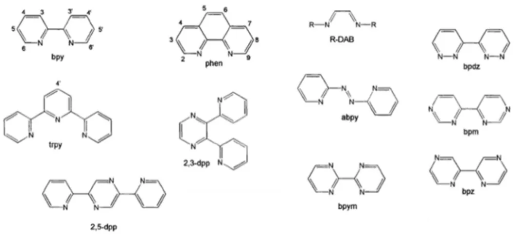
An improvement of charge transport through the molecular wire can also be achieved by adding along the organic skeleton some photoactive centres, which upon irradiation undergo light-induced excitation; with the appropriate molecular systems, charge dissociation could follow photoexcitation, with subsequent photocurrent generation.[137-143] To this aim, many transition metal complexes are perfect candidates, because they can provide both a redox-centre, for charge transport improvement, and light-induced activity.[144-146] Among the most exploited coordinating ligands for those metal complexes, neutral sites of basic di- and trigonal nitrogen are often the preferred choice;[147] metal complexes with ligands such as bipyridine or terpyridine show exceptional rich electron-transfer chemistry, which makes them systems of election for application and studies on molecular-scale charge transport.[148]
The coupling between current flow and photo-responsivity eventually leads to photoactive conductive molecular wires, which - once integrated on suitable surfaces - can be used for the preparation of nanometric solid state photoresponsive molecular junctions,[18] consisting in a thin film of light-sensitive molecules densely packed between two electrodes. This molecular layer, “encrusted” with photoactive centres, is sensitive to light-induced excitation, which leads to charge dissociation and subsequent collection at the electrodes, making this system suitable for working as optoelectronic switch or optically responsive memory, or in electric current production from solar energy conversion. Very good candidates as convenient substrates for a winning match between molecular and surface properties are transparent conductive oxides (TCOs): the transparency in the visible range, coupled with their electrical conductivity (and also the relative cheaper manufacturing costs, with respect to noble metal substrates) make these oxides “active” substrates more than just a “solid support” for the assembly of functional molecules.