Università degli Studi di Ferrara
DOTTORATO DI RICERCA IN
SCIENZE CHIMICHE
CICLO XXIII
COORDINATORE Prof. Carlo Alberto Bignozzi
Photoelectrochemical hydrogen production
from aqueous solution employing
nanostructured semiconductors
Settore Scientifico Disciplinare CHIM/03
Dottorando Tutore
Dott. Cristino Vito Prof. Bignozzi Carlo Alberto Dott. Caramori Stefano
INDEX
Chapter 1 Introduction
1.1 Hydrogen Production with Nanostructured and Sensitized Metal Oxides 3 1.2 Dye sensitized Photoanodes for water oxidation and hydrogen evolution 14 1.3. Highly Ordered semiconductors nanostructures based on TiO2 23 1.4 Experimental conditions for electrochemical titania nanotube formation 27
1.5 Bibliography 33
Chapter 2 Functionalization of titania photoelectrodes with Group VI
semiconductors
2.1 Introduction 36
2.2 Methods of functionalization of titania substrates 40
2.3 Bi2S3/TiO2photoelectrodes 42
2.4 CdS and CdSe/TiO2 photoelectrodes 50
2.5 CdTe 62
2.6 Bibliography 65
Chapter 3 Photoelectrochemical Properties of Nanostructured WO3 Prepared with Different Organic Dispersing Agents
3.1 Introduction 67
3.2 Synth-1 and Synth-2 68
3.3 Morphological Properties 72
3.4 Bibliography 89
Chapter 4 Efficient Photoelectrochemical Water Splitting by Anodically Grown
WO3 Electrodes
4.1 Introduction 92
4.2 Experimental Section 96
4.3 Results end Discussion 99
4.3.1 Anodic Formation of WO3 99
4.3.2 Photoelectrochemistry 111
4.4 Conclusions 132
4.4 Bibliography 133
Chapter 5 Photoelectrochemical behaviour of sensitized TiO2 photoanodes in aqueous environment: application to hydrogen production
5.1 Introduction 136
5.2 Experimental Section 142
5.3 Results and Discussion 145
5.3.1 Organic Sacrificial Agents 147
5.3.2. Halides 152
5.4 Conclusion 165
5.5 Bibliography 166
Chapter 1: Introduction
1.1 Hydrogen Production with Nanostructured and Sensitized Metal
Oxides
The phenomenology of semiconductor-liquid interfaces represent a very interesting and important area in science and technology[1], involving principles of electrochemistry, photochemistry, solid state theory and surface and interface science. The applications are varied, but most are focused on solar energy conversion schemes, through the use of regenerative photoelectrochemical cells (PEC), which convert sunlight to electricity or photoelectrolytic or photoelectrosynthetic cells in which solar energy is stored into chemical fuels[2]. Other important applications involve the development of photocatalytic processes for selective photooxidation of organic compounds and for environmental remediation.
Photoelecrolysis of water using sunlight[3-5] is extremely attractive for a number of reasons: (1) photoproduced hydrogen is a valuable fuel and energy carrier which can be stored more easily than electricity or heat; (2) it is non polluting, inexhaustible and flexible with respect to energy conversion in heat (combustion) or electricity (in fuel cells); (3) hydrogen is a valuable chemical by itself, being used in large quantities by the industry in chemical processing like ammonia synthesis and petroleum refining. A central concept in describing the interaction of a semiconductor with an electrolyte is the equilibration of the Fermi level of the solution and of the semiconductor. Although the concept of Fermi level has been initially introduced for an electronically conducting phase, as a level for which the probability of electron occupation of a given state is ½, in our discussion the Fermi level can be conveniently identified with the electrochemical potential of electrons in the solid and of a given redox couple (O,R) in solution, where the usual free energy relationships hold. Obviously, the solution phase does not contain free electrons, but contains available electronic states (in the form of oxidized (O) and reduced species (R) which can equilibrate with free electron in the solid. As a
consequence R o redox C C KT ln 0
of the oxidized and reduced form respectively. Under equilibrium conditions EF(solid) = EF(solution) = redox = neUredox where U is the redox potential of the couple and n is the number of exchanged electrons (e). Thus when a n-type semiconductor is brought in contact with a redox couple, electrons (majority charge carriers) from the solid pass to the solution until the two Fermi levels are identical. Due to the relatively small charge carrier density in the solid, a positive space charge layer of the typical thickness of 10-6 -10-8 m [6] is formed near the surface which is balanced by negative charges in the “compact” Helmholtz layer. The field generated by these negative charges causes an upward bending of the energy band (Fig.1.1b). A conceptually similar situation is established for a p-type semiconductor, in which the majority carriers are holes instead of electrons. In that case a space charge layer of opposite sign (negative) would be created by hole transfer to the electrolyte.
Fig.1.1 Before (a) and after (b) dark equilibration of an n type semiconductor with the electrolyte
containing a redox couple of potential U.
Energy eUredox Ec Ev EF EF Ec Ev eUredox eΦ semiconductor solution semiconductor solution + + + + + -+ + + + + -B -A + + +++ -+ ++
-The thermodynamic upper limit to the energy that can be extracted by the semiconductor/liquid junction is given by eΦ = Ec -EF = Ec + eUredox which is called the equilibrium barrier height. For all semiconductor/liquid junction the condition eUredox ~ Ev gives a barrier height approximately equal to the band gap, maximizing the power output of the system.
For semiconductors under illumination, the quantity related to Φ is the open circuit photovoltage (Voc) which reflects the maximum free energy that can be harnessed by the junctions. However the usable free energy collected across a semiconductor/electrolyte junction is not purely limited by thermodynamic quantities, but also by electron transfer kinetics and transport of the photogenerated charge carriers (Fig. 1.2). The electric field inside the space charge region may have a relevant role in assisting the charge separation at the interface. Holes are attracted towards the electrolyte by the negative charge layer, while electrons are repelled from the surface. As a consequence, photooxidation reactions can take place under illumination at the surface of an n-type semiconductor, while photoreduction can be carried out at a counter electrode (either p type semiconductor or metal electrode) wired to the photoactive material. However, in many nanostructured photoelectrodes the small size of the nanocrystals and a lower charge carrier density cannot sustain a relevant electric field[7] and the charge separation is mainly determined by kinetic reasons related to the chemical nature of the redox processes at the semiconductor/electrolyte interface: the efficiency of charge separation is thus essentially determined by the different overpotentials for the oxidation and reduction reactions taking place at the semiconductor surface and by the kinetic competition between recombination and successful transfer of the charge carriers[8,9].
Fig.1.2. Recombination pathways of photogenerated charge carriers (e- and h+) in a n-type
semiconductor in the presence of a space charge region and of a A/A- redox couple. The electron/hole pair can recombine in bulk (ibr), depletion layer (idr) or through surface states (iss). Electron can also tunnel to the electrolyte through the barrier layer (it) or across the interface (ite). The bold arrows indicate processes favorable to the functioning of the photoelectrochemical cell :hole transfer to the electrolyte and electron migration/diffusion through the bulk of the solid to the charge collector. From S.Maldonado et al., Nanostructured Photoelectrochemical Systems for Solar Photon Conversion, Imperial College Ed., London, 2002)
Several approaches to photoelectrolysis are possible, involving a photoactive semiconductor electrode electrically connected to a metal electrode, or photoactive anode (n-type) and cathode (p-type) acting either as separate electrodes, or coupled to form a monolithic structure called photochemical diode.
A common photoelectrolysis configuration, useful for the general scope of our discussion, is represented by the wiring of an n-type semiconductor, acting as a photoanode, to a metal counter electrode (Fig.1.3).
Fig.1.3 Energy level diagrams for a semiconductor-metal photoelectrolysis cell: (a) no contact, (b)
equilibrium in the dark, (c) high intensity irradiation, (d) high intensity irradiation with anodic bias.
The Fermi level in the electrolyte has been left undefined since it depends on the initial relative concentrations of H2 and O2 in solution. Fig.1.3b shows the situation at equilibrium in the dark once the semiconductor and the metal are brought in contact with the electrolyte and a depletion layer is formed near the semiconductor surface. Fermi levels of the three phases equilibrates giving rise to a band bending in the semiconductor. When the semiconductor is irradiated with photons of energy corresponding to the band-gap, electron- hole pairs are created and the Fermi level in the semiconductor is raised towards the flat band potential Vfb by an amount Vph which is the photopotential generated. The maximum value the Fermi level can reach in the semiconductor is the flat band potential Vfb which, in the case shown, is lower with respect to the H+/H2 redox couple. This means that hydrogen evolution cannot take place at the metal electrode even at the highest irradiation intensity. For hydrogen
EF EF EF A B C e- H+/H 2 EF h Vph H+/H2 O2/H2O H+/H2 O2/H2O Eg 1.23 eV H+/H2 O2/H2O D a c h+ e -Vbias h Vfb h+ O2/H2O
evolution to occur, a positive bias must be applied to the semiconductor electrode as shown in Fig.1.3c. This bias, which is usually provided by an external voltage source, should also account for the necessary cathodic (c) and anodic (a) overvoltages in order to sustain the current flow. This situation represents a condition which is frequently met with visible absorbing semiconductor metal oxides photochemically stable in aqueous environment, like WO3 or Fe2O3.
The ideal situation would be to operate with metal oxides in which, like SrTiO3[10] or KTaO3, the flat band potential is above the H+/H2 potential (Fig.1.4), therefore no external bias is required to generate H2 and O2. Unfortunately most of these materials have large band gaps (3.2-3.5 eV) which result in very low solar absorptivity and are inefficient for solar energy conversion.
Fig.1.4 Photoelectrolysis of water using a SrTiO3 photoanode. Due to the position of conduction and valence band edges hydrogen and oxygen are evolved without need of external bias. From A.Nozik and R.Memming, J.Phys.Chem., 100, 31, 1996.
The development of a stable semiconducting material that functions efficiently under visible light, which represents almost half of the available solar spectrum, is indispensable for the practical use of solar energy. Domen et al. [11] recently reported several oxynitrides of transition metals as potential candidates for visible light induced water splitting [12-14]. The conduction band edges of these oxynitrides consist predominantly of empty orbitals of the metal, resulting in similar energy levels to those of corresponding metal oxides. On the other hand, the valence bands of oxynitrides are more negative than those of oxides due to the hybridization of N 2p with O 2p orbitals. Consequently, some oxynitride materials possess appropriate band levels for water splitting, as well as a narrow band gap allowing visible light absorption. For example, tantalum oxynitride TaON (band gap: ca. 2.5 eV, corresponding to light absorption up to 500 nm) has conduction and valence band edges at ca. -0.3 and +2.2 V vs NHE, respectively, which are suitable for both water reduction and oxidation [15]. This implies that a TaON photoelectrode has the potential to produce H2 and O2 from water under visible light, even without an externally applied bias. In contrast, visible light-sensitive oxide semiconductor electrodes, such as WO3, Fe2O3 and BiVO4, require a considerable applied bias to produce H2, because their conduction band levels are too low for water reduction [16-18] Although there have been a few reports of the fabrication of n-type photoanodes based on metal oxynitrides, such as TaON or LaTiO2N, their efficiencies were still low [19-21] Furthermore, all these reports demonstrated only a photocurrent, without confirming appreciable O2 evolution.
Besides a difficult preparation route which involves the use of gaseous ammonia at high temperature (>1000K) under controlled conditions, TaON requires the use of a co-catalysts, ie. IrO2, to successfully transfer the hole to the electrolyte. Only at these conditions the requirements of efficient photolectrolysis are met.
Moreover, instability arises from the oxidation of nitrogen anions N2 by photogenerated holes (2N3- + 6 h+ N2). IrO2 loading noticeably suppressed the decreases in both photocurrent and N content. IrO2 loading most likely resulted in hole scavenge to the IrO2 particles, preventing self-oxidation of the TaON surface. The number of electrons passing through the outer circuit in 1 h (11.72 C, corresponding to 121.5 μmol of electrons) exceeded the molar amounts of both TaON (ca. 14.2 μmol) and IrO2 (ca. 0.04
from photocatalytic water oxidation, not merely the self-oxidative decomposition of the TaON material itself (Fig. 1.5).
Figure 1.5. (A) Current-potential curves in aqueous 0.1 M Na2SO4 solution (pH 6) under chopped visible light irradiation (λ > 400 nm) for TaON electrodes as-prepared (i), treated by TaCl5 (ii), heated in NH3 (iii), and loaded with IrO2 (iv). (B) Incident photon to current efficiency (IPCE) spectrum of IrO2-TaON electrode with various applied potentials (1 M Na2SO4, pH 6) and absorption spectrum of TaON (dashed line).
Other materials for stable overall water splitting under visible light are GaN and ZnO that is expressed as (Ga1–xZnx)(N1–xOx) [22–24]. Both GaN and ZnO are well-known III–V and II–VI semiconductors that have been the target of extensive research as functional materials in light-emitting diodes and laser diodes [25,26]. As shown in (Fig. 1.6), the (Ga1–xZnx)(N1–xOx) solid solution possesses a wurtzite crystal structure similar to GaN and ZnO, and is typically synthesized by nitriding a mixture of Ga2O3 and ZnO powders. As both GaN and ZnO have band-gap energies of greater than 3 eV, neither can absorb visible light in pure form. Interestingly, however, the solid solution, (Ga1– xZnx)(N1–xOx), has a band gap smaller than 3 eV and a steep absorption onset in the visible region. As shown in (Fig. 1.7), the band-gap energy (light absorption edge) is dependent on the compositional parameter (x) that is controllable by modifying the preparation parameters, and the decrease in band-gap energy in the solid solution is due to the electronic behavior of the constituent Zn and O species [27- 29].
With photoelectrochemical cells made of n-type and p-type semiconductors in contact with an electrolyte, the requirement of an external bias can be eliminated[30]. A first example of these p-n photoelectrolysis cells was reported by Nozik in 1976[31] with a n-TiO2/p-GaP heterotype device whose efficiency at zero bias was 0.25%. The energy diagram of such a cell, also called photochemical diode, is shown in Fig. 1.8. Several
other systems have been studied including n-TiO2/p-CdTe, n-SrTiO3/p-CdTe, n-SrTiO3/p-GaP, n-Fe2O3/p-Fe2O3, n-TiO2/p-LuRhO3[32]. However, many visible
absorbing p type semiconductors have shown limited stability in aqueous solvents[33], and, although power conversion efficiencies exceeding 12 % could be achieved in monolithic multijunction systems[34], the durability of many devices was low, with degradation occurring on the time scale of hours.
Figure 1.8 Energy level diagram for a p-n type photoelectrolysis cell.
An interesting approach to overcome limitations arising by the need of a bias while keeping an effective light absorption in the visible region is the absorption of dye molecules on the surface of a wide band gap semiconductor with an appropriate band energy, like TiO2 for example, which, upon light excitation, can inject electrons (in
n-H+/H2 O2/H2O
e
-h+ n-type p-typeE
F a ch
h’
Vfb(n) Vfb(p) h+e
-type materials) or holes (in p--type systems) into the acceptor states of the solid. In principle the photoxodized (photoreduced) dye can oxidize (reduce) water, while the complementary redox process can occur at the counter electrode of the cell. Although such approach has evident limitations related to the demanding 4-electron kinetics of water oxidation, some recent fundamental work pointing out the feasibility of molecular dye sensitized solar water splitting by exploiting certain specific hole transfer catalysts, are briefely reviewed in the next section. The attention will then focus on the design and characterization of newly developed photoanodes, based on anodically grown wide band gap semiconductors with improved charge transfer kinetics, as well as on the coupling of these substrates to lower band gap semiconductors.
1.2 Dye sensitized Photoanodes for water oxidation and hydrogen
evolution
In a generic sensitized PEC design, the molecular excitation and excited state formation are followed by electron transfer injection into the conduction band of a semiconductor. In order to promote multi-electron transfer events like water oxidation, multiple redox equivalents must be concentrated in a single site or cluster. The working principles of the cell are schematized in Fig. 1.9, where solar energy is stored to create a photopotential for water splitting[35,36]. In principle, at the cathode, water or CO2 reduction may occur, giving rise to the production of fuels.
Fig. 1.9 Working principle of a sensitized PEC cell for water splitting. Catox and Catred are catalyst for
water oxidation and reduction. Acc. Chem.Res. 42, 1954, 2009.
The blue dimer cis,cis [(bpy)2(H2O)Ru(III)ORu(III)(OH2)bpy)2]4+ (Fig. 1.10) was among the first molecular species to show a catalyzed water oxidation by Ce(IV) through a reaction mechanism which has been elucidated in detail by spectroscopic, electrochemical and chemical mixing experiment[37](Scheme 1). The key point is the 4 e-/4H+ loss to form the activated catalyst [(bpy)2(H2O)Ru(V)ORu(V)(OH2)bpy)2]4+ which undergoes water attack on one of the Ru(V)=O sites to give a peroxido intermediate which releases oxygen and gives back the initial Ru(III)-O-Ru(III) species on a millisecond time scale.
Fig. 1.10 Energy minimized structure of the “blue Ru dimer” cis,cis [(bpy)2Ru(OH)ORu(OH)(bpy)2]4+.
The green balls are the Ru(III) centers.
Scheme1. Mechanism of water oxidation by [(bpy)2(H2O)Ru(V)ORu(V)(OH2)bpy)2]4+. Jurss et.Al, Inorg.
As a catalyst, the blue dimer has limitations due to oxidatively induced coordination of anions which slow down the catalytic cycles. Since the O-O bond forming step occurs on single Ru(V) site, it has been demonstrated that simpler and more robust mononuclear Ru(III) aquo complexes of the type [Ru(tpy)(bpm)(H2O)]2+, where tpy is the 2,2’6’2’’ terpyridine and bpm is the bipyrimidine ligand, can undergo hundreds of turnovers without showing decomposition according to the cycle schematized in Scheme 2[38]. It must be noted that the Ru(III) state appears to be a “missing” state due to instability toward the disproportionation to Ru(IV) and Ru(II).
DFT and spectroscopic results indicate that, following the attack of water to the Ru(V)=O sites, one has the formation of a first intermediate described as a terminal peroxide coordinated to Ru(III) which undergoes further oxidation by Ce(IV) to give a 7 coordinated Ru(IV) complex where O22- acts as a chelating ligand. Oxygen can be evolved both from [Ru(IV)OO]2+ and [Ru(V)OO]3+ structures following water attack.
Scheme 2. Ce(IV) water oxidation catalyzed by by [Ru(tpy)(bpm)OH2]2+. Concepcion et al, Acc. Chem.
Although the electrocatalytic water oxidation by blue dimer has been demonstrated at FTO and ITO electrodes modified with phosophonated Ru(II) tris-bipyridine derivatives working as a redox mediator[39], the realization of an efficient dye sensitized PEC device for water oxidation has yet to be realized, but progresses are underway. Infact several issues have to be contemporarily satisfied to realize an efficient solar device: (I) effective Visibile-NIR absorption by the molecular sensitizer; (II) excited state quenching by electron transfer to the semiconductor; (III) efficient and repeated single photon-single hole transfer to the catalyst to achieve the accumulation of three oxidative equivalents to give Ru(V)-OO which undergoes attack by water giving Ru(III)-OOH; after two further subsequent oxidations, one finally obtains the evolution of molecular oxygen and the recovery of Ru(III)-OH which initiates a new catalytic cycle. While oxidative excited state quenching by Ru(II) chromophores on TiO2 have been reported to be extremely fast, the subsequent hole transfer are in critical kinetic competition with photoinjected electron (TiO2)/hole recombination. A further complication arises from the light harvesting competition between the photoactive Ru(bpy)3 type unit and the catalyst, which being relatively remote from the semiconductor surface does not contribute significantly to the photocurrent. Infact, APCEs (absorbed photons to electrons conversion efficiency) of the order of 3-4 % (Fig. 1.11b) and of 1-2 % have been achieved in the presence of hydroquinone and pure water repectively, by using the sensitizer/oxygen evolving catalyst dyad [(4,4′((HO)2P(O)CH2)2bpy)2Ru(II)(bpm)Ru(II)(Mebimpy)(OH2)]4+ (Fig. 1.11a), where Mebimpy is 2,6-bis(1-methylbenzimidazol-2.yl)pyridine)[36].
Fig. 1.11
(a) Structure of [(4,4′((HO)2P(O)CH2)2bpy)2Ru(II)(bpm)Ru(II)(Mebimpy)(OH2)]4+ sensitizer/catalyst
assembly anchored to a TiO2 electrode; (b) APCE and absorption spectrum in the presence of 0.5 M
hydroquinone acting as an electron donor in 0.1 M HClO4.
Conceptually similar approaches have been based on different molecular catalysts or nanomaterials chemically coupled to the molecular sensitizer.
In a recent interesting design[40], a manganese cage complex catalyst ([Mn4O4L6]+, or
“cubium”, L = MeOPh)2PO2--) able to undergo multiple proton coupled electron transfer, is encapsulated in a nafion membrane which has the role of providing both an high local surface concentration of redox active catalyst and a reasonable coupling with the Ru(II) dye sensitizer (Fig. 1.12). The molecular level solar water splitting, recalling that occurring in natural photosynthesis was thus beautifully demonstrated, but also in this case the performances were far from a practical application of the device, with IPCEs (IPCE=number of electrons/number of incident photons) below 2 %, corresponding to a stable photocurrent, with no externally applied bias, of the order of 30-5 μA/cm2 depending on the illumination intensity and spectral bandwidth.
Fig. 1.12 (a) IPCE Spectrum (blue) of the sensitizer/catalyst system (b) compared to that of the plain
nafion/TiO2 electrodes. (C) Pictorial scheme of working principles of the dye sensitized PEC for solar
Another interesting configuration, which is discussed in detail in another section of this book, involves the anchoring of hydrated IrO2 nanoparticles to a phosphonated Ru(II) sensitizer modified with malonate binding groups (Fig. 1.13) [41,42]. The hole transfer to the IrO2 takes place on a millisecond (2.2 ms) time scale, while charge recombination occurs on a sub-millisecond (0.37 ms) time scale. Thus, the competition between hole transfer and recombination is unfavorable to an effective charge separation. Nevertheless, under a small positive bias (≥ 330 mV) a stable photoanodic current of the order of few tens of microamperes is effectively detected, indicating the occurrence of photoinduced water oxidation under steady state conditions. Although the efficiency is low, the device represent a successful proof of concept of water splitting in a sensitized PEC device. Possible efficiency improvements could be related to synthetic modifications of the sensitizer/catalyst assembly, aimed to improve the binding between the photoactive dye and the IrO2 nanostructures, to slow down recombination and to speed up the hole transfer to Ir(IV) for improving the turnover number which is now poor (<20).
Fig. 1.13 Top: schematic diagram of a IrO2 catalyzed water-splitting dye-sensitized solar cell. Following
light excitation and oxidative quenching of the excited state of Ru(II), the hole is transferred to Ir(IV),
activating the IrO2 catalyst toward water oxidation. Bottom left: photocurrent transient showing a steady
state photocurrent. Bottom right: energy diagram and time constants for the relevant interfacial electron transfer and excited state deactivation processes.
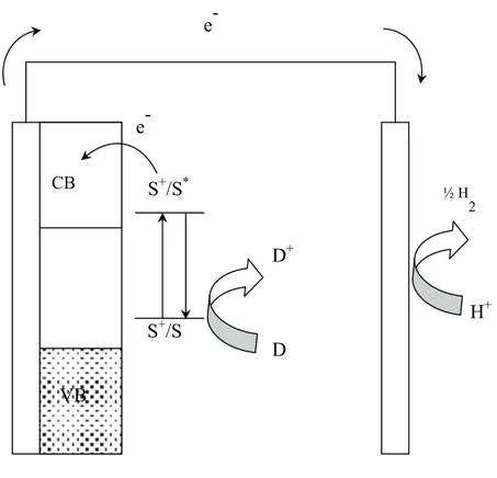
Unless sensitizers capable of performing directly an efficient water oxidation are designed, the use of sacrificial agents, although disadvantageous, cannot be avoided. It must be noted that there is a potentially large number of relatively abundant easily oxidizable ions and organic species that could be consumed to produce hydrogen. This type of conceptually simple sensitized photo-electrolytic cell is schematized in Fig.
counter electrode, thus decreasing the hydrogen yield, however this process can be avoided, or at least minimized, by an appropriate choice of D (eg. irreversible couples, non electro-active oxidized species) or simply by operating the two electrodes in separate compartments connected by a glass frit, a proton permeable membrane or a salt bridge
Fig. 1.14 Working principle of a dye-sensitized photoelectrolytic device based on a sacrificial agent.
S+/S S+/S* D+ VB CB D e -e -½ H 2 H+
1.3 Highly Ordered semiconductors nanostructures based on TiO
2Highly organized and ordered substrates produced by electrochemical formation or by template synthesis are attracting significant interest from the scientific community[43,44]. While fundamental efforts are being directed towards the understanding of self organization phenomena, technological implications are arising form the exploitation of structure-related peculiar properties which allow for promising applications in catalysis[45], photonic materials[45] and optical waveguides[46] and, particularly, in photoelectrochemistry[47]and photovoltaics[48], since grain boundaries, normally occurring between more conventional sintered nanoparticles, can be avoided or reduced.
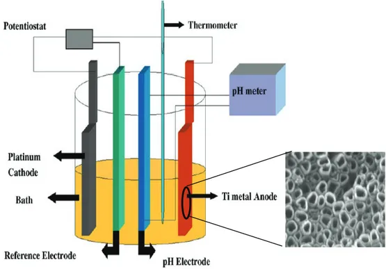
Although several attempts successfully achieved the production of nanotubes, their relatively short lengths (tens or hundreds of nanometers) [49] somehow limited their applications. However, in recent years, mainly P. Schmucki and C.A. Grimes have shown the possibility of growing high aspect ratio TiO2 nanotubes of considerable length and uniform pore diameter by tailoring the electrochemical conditions during the anodization of metallic titanium foils[50-52] (Fig. 1.15).
Fig. 1.15 Schematic apparatus for the electrochemical growth of titania nanotubes (right). From Grimes
In general the key process for anodic formation of titania nanotubes are: (1) metal oxide formation due to reaction of titanium with O2- or OH-. These anions can also migrate through the initially formed oxide layer reaching the metal/metal oxide interface where they react with the metal; (2) Ti4+ migration from the metal to the metal oxide interface under the intense electric field; (3) field assisted dissolution of the oxide at the oxide/electrolyte interface: under the intense electric field the Ti-O bonds are polarized and weakened promoting dissolution of metal cations (Ti4+); (4) chemical dissolution of titania in the HF containing electrolyte, which plays a key role in the formation of tubes rather than of an irregular mesoporous structure. Although the field assisted dissolution is initially dominating, due to the strong field across the initially thin oxide layer, it is the chemical reaction with fluorides that gives rise to localized dissolution of the oxide forming pits that act as a pore forming centers, according to
TiO2 + 6 F- + 4 H+→ TiF62- + 2H2O
The thinner barrier layer at the bottom of the chemically etched pits leads to a localized increase of the electric field which promotes field assisted dissolution leading to pore deepening and widening, while, at the same time the density of the pits increases finally leading to the full development of a densely packed nanotube array (Fig. 1.16). When the rate of chemical oxide dissolution at the mouth of the tube (top surface) becomes equal to the rate of inward movement, the thickness of the tubular layer ceases to increase. High anodization voltages increase the oxidation and field assisted dissolution, hence a grater nanotube length can usually be achieved before equilibrating with the chemical dissolution.
Fig. 1.16 Schematic diagram showing the nanotube on anodized titanium foil: (a) oxide layer formation;
(b) pit formation; (c) growth of pit into pores; (d) regions between the pores undergo oxidation and field assisted dissolution; (e) developed nanotube array. From Grimes at Al., Sol. Energy Materials & Solar Cells, 2006, 90, 2011.
As pointed out by Schmuki, another key parameter to achieve high aspect ratio nanotubes consists in adjusting the dissolution rate of TiO2 at the pore bottom while a relatively protecting environment, in which the TiO2 dissolution is slower compared to the bottom, is maintained at the walls and at the mouth of the tube (Fig. 1.17). The self acidification of the pore bottom occurs, mainly due to the electrochemical oxidation of elemental titanium, according to
Ti + 2H2O → TiO2 + 4H+
Hence it is possible, by operating in a buffered solution, to produce protons where is needed by adjusting the anodic current flow to an ideal value. Thus, while lower pH values can be obtained at the tube bottom, in turn favoring chemical dissolution of the oxide due to the “in situ” formation of HF, higher pH values and, consequently, a slower oxide dissolution rate can established at the top and at the walls of the nanotube,
thanks to the presence of pH buffering species (NH4F, (NH4)2SO4). The pH gradient (Fig. 1.17) has been calculated in great detail by using finite-difference numerical simulation, and it has been shown that a pH variation from 2 to 5 occurs by moving from the bottom to the top of the tube, corresponding to a 20 fold drop in the local chemical etching rate.
Fig. 1.17 Schematic representation of: (a) oxide formation and dissolution reactions; (b) pH profile
within the pore; (c) dissolution rate (proportional to the arrow length). From Schmucki et al., Angew. Chem. 2005, 44, 2100.
1.4 Experimental conditions for electrochemical titania nanotube
formation
In general potentiostatic or potential sweep methods are preferred over a galvanostatic approach which has the tendency to oscillate and destabilize the steady state conditions within the pore. A method devised by Schmucki et. al[50], involves the use of an aqueous electrolyte containing 1 M (NH4)2SO4 and smaller amount of NH4F (0.5-5% w/w ). The electrochemical treatment consists in a voltage ramp from open circuit potential to 20 V, adopting various scan rates, followed by a potentiostatic treatment at 20 V for different times.
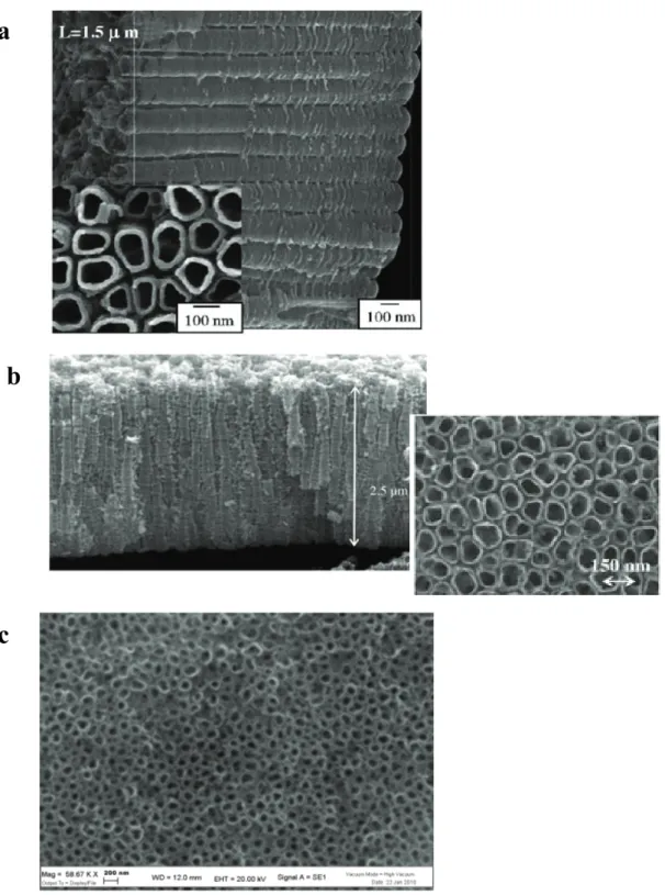
Considering, water based electrolytes, Grimes at al. [51]achieved the best results (i.e. nanotubes up to six microns long) in a solution containing either fluoride salts (NaF or KF) or HF, in the presence of buffer salts like sodium sulfate, or sodium or potassium hydrogen phosphate in a pH interval ranging from 3 to 5 (Fig. 1.18). The potential window necessary to induce nanotube formation was 10-25 volts which could be maintained for several hours, up to 25 (Tab.1). The as made nanotubes present an amorphous structure which crystallizes at high temperature ( > 280 C°) to give anatase and rutile. The rutile phase becomes dominating at temperatures higher than 620 C°.
Table.1 Electrolyte composition of KF based electrolytes and relative electrochemical treatment. V is constant voltage ant t is the application time. D and L stand for nanotube diameter and length, Q stands for quality of the anodized substrates. NT denotes an homogeneous nanotube coverage, No NT partially developed/porous surfaces. pH was adjusted by addition of sulfuric acid (pH 1-2) sodium hydrogen sulfate or citric acid (2.5-6.5). From Grimes et al. Sol.Energy Materials Sol. Cells, 90, 2006,2011
Fig. 1.18 Titania nanotubular arrays grown in various aqueous fluoride containing electrolytes. (a) 0.1 M
F- + 1 M SO
42- at pH 2.8 and at 25 V for 20 h; (b) 1 M (NH4)2SO4 + 0.5% NH4F (w/w) by using a
potential sweep from OCP to 20 V at 0.1 V/s; (c) 1M KF 0.5 M Na2SO4 at pH 4 at 25 V for 24 h.
a
b
Higher aspect ratio (up to an amazing 835 L/d ratio) nanotubes[52] could be obtained in organic electrolytes comprising an high dielectric constant solvent (N-methyl-formamide (NMF), Formamide (FA), dimethylsulfoxide (DMSO), ethylene glycol) a small percentage of water and fluoride salts of hydrofluoric acid. The highly polar FA and NMF increase dramatically nanotube length, probably due to an accelerated growth of the substrate. Infact, the dielectric constants of FA and NMF of respectively 111 and 182.4 are significantly higher than that of water (78.4). As a consequence, for any given potential the higher electrolytic capacitance induces a larger number of charges in the oxide layer, which in turn, promote an enhanced extraction of Ti4+. At the same time a limited presence of water reduces the oxide dissolution rate in the fluoride containing medium aiding a longer nanotube formation.
In comparison with aqueous electrolytes, the range of applied anodization potentials over which nanotube arrays are formed is significantly extended, with an upper limit of 50 V in FA and NMF electrolytes. This is consistent with a more difficult oxygen donation in comparison with water, requiring higher overvoltages to occur. However, higher anodization potentials also imply a grater driving force for both electronic and ionic conduction within the oxide layer, both factors favoring nanotube formation and growth.
The comparison between the anodization current recorded in an aqueous electrolyte and that obtained in FA-NMF solvents is indeed striking (Fig 1.19): while in aqueous environment passivation is almost immediately established, causing a quick drop in current, in FA-NMF the current remains at an high and constant level for at least 100 s, which is consistent with the formation of a thin oxide layer of high conductivity and a low titanium oxidation rate. It is the high conductivity of the oxide layer which enables a faster inward movement of the Ti/TiO2 interface, resulting in an improved nanotube length. Also DMSO is a suitable solvent for inducing long nanotube growth (Fig. 1.20), probably due to its protophilic properties which moderate the activity of HF. This minimize the loss by chemical dissolution from the tube mouth, allowing the tubes to grow deep into the titanium foil.
Figure 3.5 Figure 3.6
Fig. 1.19 Anodization current of Ti foil at constant 25 V in different electrolytic compositions: (A)
FA-NMF + NH4F; (B) NH4F aqueous; (D) KF aqueous.
A B
Fig. 1.20 FESEM images of anodically grown nanotubes in a FA based electrolyte at 35 V for 48 hours
1.5 Bibliography
(1) Ni, M.; Leung, M. K. H.; Leung, D. Y. C.; Sumathy, K. Renewable Sustainable
Energy Rev. 2007, 11, 401.
(2) Lewis, N. S. Inorg.Chem. 2005, 44, 6900-6911.
(3) Eisenberg, R.; Nocera, G. D. Inorg.Chem. 2005, 44, 6799-6801. (4) Nozik, A. J.; Memming, R. J.Phys.Chem. 1996, 100, 13061-13078. (5) Fujishima, A.; Honda, K. Nature 1972, 238, 37.
(6) Maldonado, S.; Fitch, A. G.; Lewis, N. S. Nanostructured and
Photoelectrochemical Systems for Solar Photon Conversion; Imperial College
Press: London, 2008.
(7) Sodergren, S.; Hagfeldt, A.; Olsson, J.; Lindquist, S.-E. J.Phys.Chem. 1994, 5552-5556.
(8) Gregg, B. A. Coordination Chemistry Reviews 2004, 248, 1215-1224.
(9) Gregg, B. A.; Pichot, F.; Ferrere, S.; Fields, C. R. J.Phys.Chem.B 2001, 105, 1422-1429.
(10) Kumar, A.; Santangelo, P. G.; Lewis, N. S. J.Phys.Chem. 1992, 834-842.
(11) Ryu Abe, Masanobu Higashi, and Kazunari Domen J. AM. CHEM. SOC.
2010, 132, 11828–11829
(12) Higashi, M.; Abe, R.; Takata, T.; Domen, K. Chem. Mater. 2009, 21, 1543– 1549.
(13) Maeda, K.; Teramura, K.; Lu, D.; Takata, T.; Saito, N.; Inoue, Y.; Domen, K.
Nature 2006, 404, 295.
(14) Abe, R.; Takata, T.; Sugihara, H.; Domen, K. Chem. Commun. 2005, 3829–3831 (15) Chun, W. J.; Ishikawa, A.; Fujisawa, H.; Takata, T.; Kondo, J. N.; Hara, M.;
Kawai, M.; Matsumoto, Y.; Domen, K. J. Phys. Chem. B 2003, 107, 1798–1803 (16) Santato, C.; Ulmann, M.; Augustynski, J. J. Phys. Chem. B 2001, 105, 936 -940. (17) Kay, A.; Cesar, I.; Gratzel, M. J. Am. Chem. Soc. 2006, 128, 15714–15721. (18) Sayama, K.; Nomura, A.; Arai, T.; Sugita, T.; Abe, R.; Yanagida, M.; Oi, T.;
Iwasaki, Y.; Abe, Y.; Sugihara, H. J. Phys. Chem. B 2006, 110, 11352–11360 (19) Abe, R.; Takata, T.; Sugihara, H.; Domen, K. Chem. Lett. 2005, 34, 1162–1163.
(20) Nakamura, R.; Tanaka, T.; Nakato, Y. J. Phys. Chem. B 2005, 109, 8920–8927. (21) Le Paven-Thivet, C.; Ishikawa, A.; Ziani, A.; Le Gendre, L.; Yoshida, M.;
Kubota, J.; Tessier, F.; Domen, K. J. Phys. Chem. C 2009, 113, 6156–6162 (22) Maeda K, Takata T, Hara M, Saito N, Inoue Y, Kobayashi H, Domen K (2005) J
Am Chem Soc 127:8286
(23) Maeda K, Xiong A, Yoshinaga T, Ikeda T, Sakamoto N, Hisatomi T, Takashima M, Lu D, Kanehara M, Setoyama T, Teranishi T, Domen K (2010) Angew Chem, Int Ed 49:4096
(24) Surface Nanostructures in Photocatalysts for Visible-Light-Driven Water Splitting -Kazuhiko Maeda and Kazunari Domen-
(25) Nakamura S, Mukai T, Senoh M (1994) Appl Phys Lett 64:1687
(26) Tsukazaki A, Ohtomo A, Onuma T, Ohtani M, Makino T, Sumiya M, Ohtani K, Chichibu SF, Fuke S, Segawa Y, Ohno H, Koinuma H, Kawasaki M (2005) Nat Mater 4:42
(27) Hirai T, Maeda K, Yoshida M, Kubota J, Ikeda S, Matsumura M, Domen K (2007) J Phys Chem C 111:18853
(28) Jensen LL, Muckerman JT, Newton MD (2008) J Phys Chem C 112:3439 (29) Wei W, Dai Y, Yang K, Guo M, Huang B (2008) J Phys Chem C 112:15915 (30) Fornarini, L.; Nozik, A. J.; Parkinson, B. A. J.Phys.Chem. 1984, 88, 3238-3243. (31) Nozik, A. J. Appl. Phys. Lett. 1976, 29, 150-153.
(32) Kainthla, R. C.; Zelenay, B.; Bockris, J. O. M. J. Electrochem. Soc. 1987, 134, 841-845.
(33) Grimes, C. A.; Varghese, O. K.; Ranjan, S. Light, Water, Hydrogen; Springer: New York, 2008.
(34) Khaselev, O.; Turner, J. A. Science 1998, 280, 425-427.
(35) Alstrum-Acevedo, J. H.; Brennaman, M. K.; Meyer, T. J. Inorg.Chem. 2005, 44, 6802-6827.
(36) Concepcion, J. J.; Jurss, J. W.; Brennaman, M. K.; Hoertz, P. G.; Patrocionio, A. O. T.; Murakami Iha, N. Y.; Templeton, J. L.; Meyer, T. J. Accounts of
Chemical Research 2009, 42, 1954-1965.
(37) Liu, F.; Concepcion, J. J.; Jurss, J. W.; Cardolaccia, T.; Templeton, J. L.; Meyer, T. J. Inorg. Chem. 2008, 47, 1727-1752.
(38) Concepcion, J. J.; Jurss, J. W.; Norris, M. R.; Chen, Z.; Templeton, J. L.; Meyer, T. J. Inorg.Chem. 2010, 49, 1277-1279.
(39) Jurss, J. W.; Concepcion, J. J.; Norris, M. R.; Templeton, J. L.; Meyer, T. J.
Inorg.Chem. 2010, 49, 3980-3982.
(40) Brimblecombe, R.; Koo, A.; Dismukes, C. G.; Swiegers, G. F.; Spiccia, L.
J.Am.Chem.Soc. 2010, 132, 2892-2864.
(41) Youngblood, J. W.; Anna Lee, S.-H.; Maeda, K.; Mallouk, T. E. Accounts of
Chemical Research 2009, 42, 1966-1973.
(42) Youngblood, J. M.; Seung-Hyun, A. L.; Kobayashi, Y.; Ernandez Pagan, E. A.; Hoertz, P. G.; Moore, T. A.; Moore, L. A.; Gust, D.; Mallouk, T. E.
J.Am.Chem.Soc. 2009, 131, 926-927..
(43) Kayes, B. M.; Richardson, C. E.; Lewis, N. S.; Atwater, H. A. IEEE
Photo.Spec.Conf 2005, 55-58.
(44) Kayes, B. M.; Atwater, H. A.; Lewis, N. S. J.Appl.Phys. 2005, 97 114302, 1-11. (45) Clarke, J.; Hill, D. R.; Roberts, J. J.Chem.Technol.Biotechnol. 1997, 68, 397. (46) Haginoya, C.; Ishibashi, M.; Koike, K. Appl. Phys. Lett. 1997, 71, 2934.
(47) Mor, K. G.; Shankar, K.; Paulose, M.; Varghese, O. K.; Grimes, C. A. Nano
Letters 2005, 5, 191-195.
(48) Grimes, C. A.; Mor, G. K. TiO2 Nanotube Arrays: Synthesis, Properties and
Applications; Springer: Dordrecht, Heidelberg, London, New York, 2009.
(49) Varghese, O. K.; Gong, D.; Paulose, M.; Ong, K. G.; Dickey, E. C.; Grimes, C. A. Adv.Mater. 2003, 15, 624.
(50) Macack, J. M.; Tsuchiya, H.; Schmucki, P. Angew.Chem.Int.Ed. 2005, 44, 2100-2102.
(51) Mor, G. K.; Varghese, O. K.; Paulose, M.; Shankar, K.; Grimes, C. A. Solar
energy Materials and Solar Cells 2006, 90, 2011-2075.
(52) Paulose, M.; Shankar, K.; Yoriya, S.; Prakasam, E. H.; Varghese, O. K.; Mor, G. K.; Latempa, T. A.; Fitzgerald, A.; Grimes, C. A. J.Phys.Chem.B. Letters 2006,
Chapter 2: Functionalization of titania photoelectrodes with
Group VI semiconductors
2.1 Introduction
Group VI semiconductors, where a metal Mn+ ( M = Cd2+, Bi3+, Cu2+, Pb2+) is combined with S2-, Se2-, Te2- to form an M2(S,Se,Te)n solid may offer interesting possibilities when employed in photoelectrolytic or photoelectrosynthetic devices applied to solar hydrogen production. Although in many of these semiconductors the quasi-Fermi energy of the photogenerated hole is too low to drive an efficient water oxidation, they can be advantageously used for the photoinduced oxidation of Na2S or of other easily oxidizable molecules or ions resulting in the concomitant production of hydrogen at the cathode of the photoelectrochemical cell[1-3].
It must be noted that H2S and sulfides are common, abundant and harmful contaminants present in fossil fuels and in natural gas, where H2S alone can account for up to 30 % of their total volume[4].
Thus, by exploiting solar energy and chalcogenide semiconductors, sulfides can be photoelectrochemically converted to less dangerous oxidized forms (i.e. polysulfides, Sn2-) and to molecular hydrogen thanks to an energy storing cycle which can be proposed as an interesting method for the photodegradation of H2S wastes according to the following simplified photocatalytic scheme, where CdS is chosen as an example of photoactive semiconductor:
H2S + 2 NaOH → Na2S + 2 H2O
CdS + hν → h+(CdS) + e-(CdS) (anode) 2h+ (CdS) + S2- (aq) → S + 2 CdS (anode) 2 e- + 2H2O → H2 (g) + 2 OH- (aq) (cathode)
Thus, the overall reaction is the splitting of H2S in S (or more appropriately in Sx2-, given the excess of S2- in solution) and H2. At the end of the photoelectrolysis one also retrieves the base which has been initially used to convert H2S into a water soluble sulfide salt, in which it is obviously easier and safer to handle.
Generally, group VI semiconductors are characterized by a relatively small band gap (from 2.4 eV for CdS to 1.4 eV for Bi2S3) and by intense direct transitions which allow for an efficient visible light absorption from relatively thin (few hundreds nm) layers of photoactive substrate[5]. Since in the presence of S2- and at an appropriate pH, the Fermi level of these semiconductors is more negative than that of TiO2 they can be used as photosensitizers to extend the spectral sensitivity and responsivity of TiO2 electrodes which merely act as electron gathering mediums (Fig.2.1a). The possibility of obtaining inter-particle electron transfer has possible important implications: the deposition of group VI semiconductors onto nanocrystalline porous TiO2 substrates (roughness coefficient 100-1000) leads to an effective light absorption from a relatively thin absorber layer (Fig. 2.1b), in which the photogenerated electron (e) and hole (h) pairs are relatively close to both the electrolytic solution containing S2- (hole acceptor) and to the electron collector, with the subsequent reduction of the probability of charge recombination.
Fig. 2.1 Sensitization of TiO2 by a visible absorbing semiconductor
Besides this effect, the coupling to TiO2 may also have a relevant stabilizing effect against the photochemical degradation of semiconductors like CdS or CdSe. While the self oxidation of the lattice sulfides by photogenerated holes can be controlled by using a high concentration of hole scavengers, like S2-, the trapping of electrons, responsible for the irreversible Cd2+/0 reduction, can be avoided by activating the electron transfer to TiO2. Fig. 2.2 can be taken as an illustrative example of the improvement in the photoelectrode stability obtained by coupling CdS to a TiO2 substrate: while the fundamental CdS absorption at 500 nm is maintained in CdS/TiO2 systems, it is lost in
e h h e TiO2 + hν hν Group VI semiconductor TiO2 hν
200 300 400 500 600 700 800 5 10 15 20 25 30
CdS + TiO
2 R% nm before irradiation after irradiation (20') 200 300 400 500 600 700 800 0 10 20 30 40 50 60 70 80Pure CdS
R% nm before irradiation after irradiation (20')pure CdS substrates after 20 minutes of intense irradiation in a sulfide containing electrolyte. The decreased reflectance at longer wavelength is indicative of the development of a grey coloration of the photoelectrode, consistent with the formation of Cd0
a
b
Fig 2.2 Diffuse reflectance spectra of CdS based electrodes before (black) and after (red) 20 minutes of
continuos irradiation under simulated sunlight. (a) Mixed electrode: 50 % W/W nanocrystalline TiO2 and
In a similar way, the sensitization of tubular titania structures could be equally promising, since the cylindrical geometry of the TiO2 core may allow for the generation of the charge carriers at a short distance from the electron collector, regardless of the penetration depth of the radiation, leading to an enhancement in electron collection efficiency as it is pictorially illustrated in Fig 2.3.
Fig.2.3 (a) TiO2 nanotubes functionalized with group VI semiconductors; (b) generation and collection of
charge carriers.
TiO2 nanotubes
To electron collector ( Ti foil )
visible absorbing semiconductor : CdS, CdSe, CdTe, Bi2S3 h e e h h
a b
e h e2.2 Methods of functionalization of titania substrates
Sulfur, Selenium and Tellurium have very similar chemical properties: many sulfides and selenides are insoluble compounds (ks(CdS) = 10-26, ks(Bi
2S3) = 10-98 e ks(CdSe) = 10-33) hence it is possible to obtain the functionalisation of titania electrodes by a simple chemical bath deposition.
Many methods of obtaining a CdS deposition on a variety of substrates have been devised[6-8] and all of these reside in the in situ reaction of S2- with Cd2+, which can be obtained by alternated repeated immersion of the photoelectrodes in separate solutions containing Na2S and Cd(NO3)2 or CdCl2. An analogous procedure can be adopted for depositing Bi2S3, starting from Bi(NO3)3 or Bi(Ac)3 (Ac=acetate) solutions. A convenient and stable selenide source for CdSe deposition can be represented by sodium selenosulfite (Na2SeSO3) which can be obtained by reaction of elemental selenium with a 4 fold excess of Na2SO3 at 70-80 °C. In the presence of Cd2+, SeSO3 2-gives a grayish precipitate which quickly decomposes, particularly under moderate heating (ca. 50 °C) to give red-brown CdSe[9,10].
In general, a thermal treatment in air improves the performance and the stability of the photoelectrodes leading to an enhancement in crystallinity, in electrical connections between the nanostructures and to an increased hole diffusion length. In the case of CdSe a partial sublimation of the photoactive film is observed starting from 260 °C. A post treatment with CdS can be helpful for encapsulating CdSe, making it more stable at elevated temperature, improving, at the same time, the photon to electron conversion at shorter wavelengths.
Bi2S3 (bismuthinite, orthorhombic) electrodes thermally degrade in air at T > 260 C° to form white bismuth oxide sulfate (Bi28O32(SO4)10) due to reaction with atmospheric oxygen. In nitrogen atmosphere the annealing can be carried out at 400 °C without observing decomposition. However, the best photoelectrochemical results were observed with photoelectrodes annealed in air at 220 °C for 15-20 minutes, in agreement with conditions reported by other authors in the preparation of TiO2 (P 25) supported Bi2S3 nanoparticles for environmental remediation[11].
The electrochemical methods of TiO2 surface modification by growth of lower band gap semiconductors rely on principles analogous to the chemical deposition, i.e. the
electrochemical generation of the anion (S2-, Se2-, Te2-) in a cation ( Cd2+, Bi2+) containing electrolyte, according to the following reactions
S + 2e- → S2-
Cd2+ (Bi3+) + S2- → CdS ( Bi2S3)
Se(Te)O2 + 6 e- + 4 H+ → Se2-(Te2-) + 2H2O Cd2+ + Se2- (Te2-) → CdSe(Te)
Compared to chemical impregnation methods, the electrodeposition may lead to more homogeneous surfaces and to a better control of the sensitizing semiconductor growth, since the anions are directly electrogenerated on the oxide surface with the desired rate. The precursor electrolytes for CdS and Bi2S3 deposition are very similar, consisting in a saturated sulfur solution in DMSO to which 0.3 M or Bi(NO3)3 are added. The CdSe precursor is composed by selenium oxide solution in sulfuric acid in the presence of Cd(NO3)2 [12]. Our preferred concentrations were 10-2 M SeO2 and 0.3 M Cd(NO3)2 in 4 10-3 M H2SO4.
The deposition can be performed by either potentiostatic, potentiodynamic (multiple scan) or galvanostatic procedures. In our case we have adopted a multiple scan deposition technique where the potential was linearly varied on subsequent cycles at cathodic potentials, usually between -0.3 and -1.1 V vs SCE, with a scan rate of 50 mV/s until strongly colored electrodes were obtained.
The deposition was considered complete when the maximum optical density (absorbance or, in the case of opaque substrates, spectral absorption) allowed for the absorption of at least 70% of the incident photons. A direct reliable estimate of the amount of deposited material from the integration of voltammetric waves was either difficult or impossible due to the capacitive TiO2 contribution, to the irreversible nature of the electrochemical process and to the lack of any clearly defined diffusion limited peak.
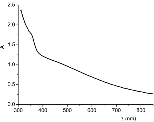
400 450 500 550 600 650 700 750 800 850 0.0 0.5 1.0 1.5 2.0 2.5 3.0 3.5 4.0 4.5 5.0 5.5 A nm)
2.3 Bi
2S
3/TiO
2photoelectrodes
The absorption spectrum of Bi2S3 chemically deposited on TiO2 nanoparticles shows a featureless continuous absorption in the whole visible region, with an estimated optical band gap of 1.4 eV (Fig. 2.4) [11,13]. Repeated (up to 40) chemical bath deposition from Bi(Ac)3 and Na2S leads to intensely colored electrodes with a maximum absorbance of the order of 4, allowing for an almost quantitative light absorption. Despite this, the chemical impregnation appears to be characterized by a scarce reproducibility, even by considering the same number and duration of the deposition steps, and the photoelectrochemical response in 0.1 M Na2S is promising but also highly variable: in the presence of a 0 V vs SCE potential bias, photocurrents ranging from 7 to 4 mA/cm2 (Fig. 2.5) were observed under a 0.2 W/cm2 visible light irradiation (HID lamp). A modest positive polarization results however in a strong enhancement of the photocurrent, which is superimposed to the contribution of the direct electrochemical oxidation of sulfides, whose onset is located at about 0.2 V vs SCE.
-0.8 -0.6 -0.4 -0.2 0.0 0.2 0 2 4 6 8 10 12 14 0.2 W/cm2 HID dark J (mA/ cm 2 ) V (V vs SCE)
Fig. 2.5 J-V characteristics under illumination (black) (0.2 W/cm2 HID lamp) and in the dark (red) of a
Bi2S3/TiO2 electrode in 0.1 m Na2S.
The electrodeposition process quickly leads (2-4 potential scans) to good quality Bi2S3 films with a good reproducibility. Although the optical density is lower than that obtained by chemical impregnation (Fig. 2.6), the Light Harvesting Efficiency (LHE) of the photoelectrodes varies between 95% and 50 % in the spectral region between 400 and 850 nm, with a sharp rise below 400 nm due to TiO2 absorption. The maximum photocurrent at 0 mV vs SCE is in the order of 5± 1 mA/cm2 in the presence of an incident irradiance of 0.12 W/cm2 (AM 1.5G). The advantage of having a panchromatic absorber is clearly evident from Fig. 2.7, where the UV component has been completely removed from the excitation light with a 420 nm cut-off filter. Under these conditions the photoelectrode does not undergo a substantial decrease in its performance, still reaching values of more than 3 mA/cm2 at 0 V vs SCE, showing that Bi2S3 is effectively injecting into the conduction band of TiO2.
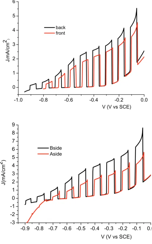
Interestingly, despite the good performances, the J-V curves recorded under shuttered illumination show a notable difference between front (electrolyte) side and backside (FTO contact) illumination evidencing a more effective photocurrent generation by
300 400 500 600 700 800 0.0 0.5 1.0 1.5 2.0 2.5 A nm)
backside illumination (Fig. 2.8). The effect is even more dramatic in thick electrodes, where the transients in front irradiation are about half of those recorded in backside mode, corroborating the indication of limitations arising from charge transport and collection. Although the J-V curves do not show dark cathodic features, usually originated from charge recombination mediated by surface states, the existence of a certain amount of electron recombination is also clearly suggested by the non ideally rectangular shape of the transients.
-0.8 -0.6 -0.4 -0.2 0.0 -1 0 1 2 3 4 5 6 J (mA/ cm 2 ) V (V vs SCE) of (/) cut 420
Fig. 2.7 JV curves of electrodeposited Bi2S3 with (red) and without (black) 420 nm cut off filter. 0.1 M
Na2.
Frontside irradiation
Backside irradiation Bi2S3/titania layer
Fig. 2.8 Shuttered J-V curves of Bi2S3/TiO2 systems in 0.1 M Na2S under Am 1.5 G illumination. (a)
thinner layer (20 deposition scans from 10-3 Bi3+ solution), (b) thicker Bi
2S3 layer (100 deposition scans
from 10-3 Bi3+ solution). -1.0 -0.8 -0.6 -0.4 -0.2 0.0 0 1 2 3 4 5 6 V (V vs SCE) back front J ( m A /cm 2 ) -0.9 -0.8 -0.7 -0.6 -0.5 -0.4 -0.3 -0.2 -0.1 0.0 -3 -2 -1 0 1 2 3 4 5 6 7 8 9 J( mA/cm 2 ) V (V vs SCE) Bside Aside
The IPCE under a potential bias of -0.5 V vs SCE is relevant when the photoelectrode is illuminated through the FTO (collector) side (backside) reaching values in the order of 30-10 % in the 350-450 nm region and extending to 830 nm (Fig.2.9). Although the UV contribution of TiO2 cannot be completely neglected, the sharp decrease in IPCE is in contrast with the absorption spectrum of Bi2S3, which decline smoothly and maintains high LHE values by moving from shorter to longer wavelengths, suggesting that high energy photons with a smaller penetration depth, being absorbed in closer proximity of the back contact are more effectively converted in electrons flowing through the external circuit. By contrast, illumination to the front side leads to an almost negligible photon to current conversion, indicating that only a small fraction of electron/hole pairs generated in the outer Bi2S3 layer is effectively capable to escape from recombination. Actually, the difference between the photocurrent measured in front and back illumination mode under full AM 1.5 (~ 100 mW/cm2) is smaller than what could be anticipated by observing the photoaction spectra recorded under a low intensity (~ 1 mW/cm2) monochromatic light. The reason is most probably related to the fact that, due to the low excitation intensity, nearly all of the monochromatic photons in the incident beam are absorbed by the most external layers of the black absorber, where the charge collection is poor, and by a lower conductivity of Bi2S3 itself, which, under a sufficiently high light intensity exhibits a photoconductor behavior object of recent investigations in the field of sensor devices[14,15].
Fig. 2.9 IPCE spectra of Bi2S3/TiO2 system biased at -0.5 V vs SCE. The negative bias is chosen from
minimizing the dark background from electrochemical oxidation of sulfides.
350 400 450 500 550 600 650 700 750 800 850 0 5 10 15 20 25 30 35 IP CE % (nm) 50 scan Aside 50 scan bside 100 scan aside 100 scan bside
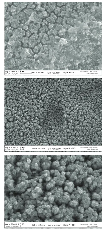
In order to improve charge collection, the electrodeposition of Bi2S3 on titania nanotubes can be successfully performed, as demonstrated by the SEM images of the top Bi2S3/nanotube structure (Fig.2.10). The multiple scan deposition at 10 mV/s from a diluted (10-3 M Bi3+) precursor electrolyte in DMSO leads to a quite homogeneous decoration of tubular nanostructures with Bi2S3, clearly evidenced by a considerable thickening of the nanotube walls, reaching a size of about 50 nm, resulting, in many cases, in the complete occlusion of the nanotube mouth. The presence of some spherical agglomerates of Bi2S3 with a diameter variable between 200 nm and 1 micron is also evident.
The photoaction spectra of the Bi2S3/nanotubes photoelectrodes (Fig. 2.11) have distinct characteristics when compared with those found for Bi2S3/nanoparticle systems: although the absolute IPCE are in the same order of magnitude, with values of 10-15% under -0.5 V vs SCE potential bias, a substantially constant photoconversion in the whole visible region is observed, as would be reasonably expected for a black absorber in which the light harvesting efficiency approaches unity. In other words, while in the planar Bi2S3/TiO2 electrodes the light collection efficiency drops dramatically, depending on the photon penetration depth and ultimately on the distance from the collector at which electron/hole pairs are generated, in Bi2S3/nanotubes the electrons are collected with analogous efficiency in both the blue and red part of the spectrum. This is consistent with the coated nanotube geometry, where, without respect to the penetration depth of the visible radiations, the charge carriers diffuse or migrate orthogonally to the tube axis[16], traversing in all cases nearly the same thickness of Bi2S3 before reaching the charge collector.
450 500 550 600 650 700 750 800 850 0.0 0.1 0.2 0.3 0.4 0.5 0.6 0.7 0.8 0.9 1.0 1.1 IPCE% / IP CE% ma x (nm) 45 scan triton X-100 45 scan
50 scan coll Bside 100 scan coll Bside
Fig. 2.10 Bi2S3/titania nanotubes surface obtained by multiple scan (45, 10 mV/s) electrodeposition of
Bi2S3 from 10-3 M Bi3+ electrolytes. Sample annealed in air at 220 °C for 30’.
Fig. 2.11 Normalized photoaction spectra: Bi2S3/titania nanotubes (black and red) compared to
2.4 CdS and CdSe/TiO2 photoelectrodes
The chemical bath deposition of CdS on titania nanotubes leads to photoelectrodes characterized by a satisfactory photoelectrochemical properties. SEM micrographs taken at 9700 X and at 51370 X indicate that after the annealing at 400 °C chemically deposited CdS forms a nanocrystalline network which covers and conglobes the anatase nanotubes which have a mouth diameter of about 100 nm (Fig. 2.12). Single CdS nanostructures cannot be resolved in SEM mode, however, higher resolution transmission microsocopy (HRTEM) studies carried out by Sun et. al. have confirmed that the initially formed CdS network consists of quantum dots whose size varies between 2 and 10 nm[17]. By contrast, the electrodeposition of CdS produces a much more homogeneous coating, which is actually difficult to detect in SEM imaging, simply resulting in a thickening of nanotube walls (Fig. 2.12c). Nevertheless, the diffuse reflectance spectrum (Fig. 2.12d) confirms without any doubt the presence of CdS, showing the typical steep and intense transition with onset located at about 600 nm, leading to a significant extension of the spectral sensitivity of the photoanode, with an effective absorption (75%-80%) of the photons in the 510-300 nm range.
a
b
Fig. 2.12 CdS modified nanotubes by (a) and (b) chemical bath deposition and (c) electrodeposition. (d)
Diffuse reflectance spectrum of the electrodeposited CdS/titania nanotubes (nt) surface compared to the unmodified titania NT surface. Titania NT were obtained from DMSO/HF anodization procedures.
300 350 400 450 500 550 600 650 700 750 800 0 10 20 30 40 50 60 70 80 R% (nm) TiO2nt + electrodepositedCdS TiO2nt c d
Fig. 2.12 CdS modified nanotubes by (a) and (b) chemical bath deposition and (c) electrodeposition. (d)
Diffuse reflectance spectrum of the electrodeposited CdS/titania nanotubes (nt) surface compared to the unmodified titania NT surface. Titania NT were obtained from DMSO/HF anodization procedures.
The photoaction spectrum of the CdS sensitized nanotubes recorded in 0.1 M Na2S at 0 V vs SCE shows a good conversion, approaching 50 % at 500 nm, in good agreement with the absorption spectrum of CdS, testifying an effective charge injection into TiO2 (Fig. 2.13). The good performance is confirmed under Am 1.5 irradiation, where phocurrents of the order of 6-9 mA/cm2 are recorded in 0.1 M Na2S (Fig. 2.13). The electrodeposited CdS substrates generate higher currents (ca. 20% higher with respect to chemically deposited substrates), but display a lower fill factor. In both cases the open circuit photovoltage is ≥ 1 V vs SCE. In the presence of a formate buffer as a sacrificial donor the photocurrents are more then doubled, reaching 16-18 mA/cm2 due both to a more effective hole scavenging which can be originated by HCOOH/HCOO- adsorption onto the CdS/TiO2 surface, and by secondary electron injection by highly reducing HCOO·intermediates which are known to inject into the conduction band of TiO2.
-1.0 -0.8 -0.6 -0.4 -0.2 0.0 0 3 6 9 12 15 18
chemically deposited HCOOH/HCOONa
chemically deposited Na2S Electrodeposited Na2S J (mA /cm 2 ) V (V vs SCE) 300 350 400 450 500 550 600 0 5 10 15 20 25 30 35 40 45 50 IP CE % nm)
Fig. 2.13 (a) Photoaction spectrum of chemically impregnated CdS/TiO2 nanotubes at 0 V vs SCE (b)
J-V curves under Am 1.5 illumination (0.12 W/cm2) in the presence of Na
2S (black chemically deposited,
Although in this case the sensitization of nanotubes with CdS produces good performances, comparable photocurrent densities (J ~ 6±1 mA/cm2 ) can be found through the sensitization via electrochemical deposition of more conventional transparent nanocrystalline electrodes made of sintered titania nanoparticles. The use of transparent CdS based electrodes has the advantage of allowing for the assembly of tandem configurations, in which two spectrally complementary photoelectrodes can be in parallel connected to sum the photocurrents (Fig. 2.14a). For example, a tandem photoanode made by a CdS/TiO2 and by Bi2S3/TiO2 heterointerfaces biased at 0 V vs SCE can generate photocurrents in the order of 12-14 mA/cm2 in 0.1 M Na
2S (Fig. 2.14b) thanks to the simultaneous exploitation of the high photon to current conversion of CdS in the blue part of the spectrum ( 300-550 nm) and of the extended spectral sensitivity of Bi2S3, which is able to capture and convert photons where CdS does not absorb, starting from 830 nm.
a
S
2-S (2-S
x2-)
2H
2O
H
2+ 2 OH
- CdS Bi2S3h
-1.0 -0.8 -0.6 -0.4 -0.2 0.0 -2 0 2 4 6 8 10 12 14 V (V vs SCE) J (mA/ cm 2 )
b
Fig. 2.14 (a) Scheme of a tandem photoelectrochemical cell based on CdS/TiO2 and Bi2S3/TiO2
heterointerfaces; (b) resulting J-V characteristic.
A panchromatic sensitization as well as a considerable efficiency in photon to electron conversion can be obtained by functionalizing titania nanostructures (nanotubes as well as nanoparticles) with CdSe. In this case both chemical and electrochemical deposition leads to morphologically similar surfaces where CdSe can be observed to decorate each nanotube. As previously observed, the electrodeposition is the preferred method for obtaining a more homogeneous coating of each nanostructure, where CdSe covers almost completely the entire length of every nanotube, occluding also their mouth (Fig. 2.15).
a
b
c
Fig. 2.15 SEM micrographs of (a) CdSe/titania nanotube heterostructures obtained by chemical bath
deposition ~ 19000 X; (b) CdSe functionalized nanotubes from electrochemical deposition at 5630 X; (c) higher magnification (23460 X) of (b).
Although a relevant loss of photoactive CdSe coating occurs by sublimation during the 400 C° annealing stage in air or under inert atmosphere (N2), the thermal treatment was found to be beneficial for both performance and stability of the photoelectrode. The optical band gap evaluated from the absorption spectrum (Fig. 2.16a) was found to be 1.65 eV, in good agreement with the literature reported values[18,19]. The IPCE extends from 310 to 750 nm keeping an almost constant plateau value which, with the annealed samples can reach 40 % (Fig.2.16b). The red shift in IPCE onset between untreated and annealed substrates is in agreement with the absorption spectra, where upon 400 C° treatment, a batochromic shift of the absorption threshold to about 750 nm can be observed. The increased IPCE indicate an efficient charge carrier transfer and a suitable band alignment at the CdSe/TiO2 interface. This features have been observed by other authors in CdSe/ZnO heterointerfaces[20], and have been explained by the loss of quantum confinement in CdSe nanoparticles which, due to the thermal formation of larger crystals, might facilitate the charge transport through the CdSe coating to the inner nanotube collector. Besides thermal sintering of the CdSe nanocrystals, other authors have attributed the increased reproducibility and durability of the photoelectrochemical response in cadmium calchogenide based PEC cells to the transition from cubic zinc blende to wurtzite structures, which becomes the dominating phase at temperatures > 350 C° [21].
300 350 400 450 500 550 600 650 700 750 800 0 5 10 15 20 25 30 35 40 45 as deposited 400 C° annealing IPC E % (nm) 350 400 450 500 550 600 650 700 750 800 0 1 2 3 4 bofore annealing after annealing KM unit s (nm)
a
b
Fig. 2.16 (a) Diffuse reflectance spectra (KM units) of chemically deposited CdSe on titania nanotubes;
-1.2 -1.0 -0.8 -0.6 -0.4 -0.2 0.0 0 2 4 6 8 10 12 electrochemical deposition chemical deposition J (m A/ cm 2 ) V (V vs SCE)
The performances under white light are satisfactory for both chemically and electrochemically deposited CdSe substrates ,showing photocurrents in the 10-11 mA/cm2 range at 0 V vs SCE and a Voc > 1 V (Fig. 2.17).
Fig. 2.17 JV curve under AM1.5G illumination (0.12W/cm2) of CdSe/TiO
2 NT photoanodes in 0.1 M
Na2S.
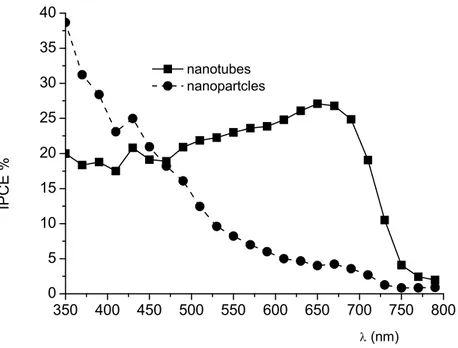
Sensitization by sequential electrodeposition of CdSe and CdS can be achieved with both colloidal (TiO2 nanoparticles) and nanotube surfaces, however, as previously observed with Bi2S3/TiO2 heterointerfaces, the comparison with the IPCE spectrum recorded for colloidal substrates in back (FTO collector) side illumination is consistent with a more favorable electron collection in nanotubular substrates, causing a broader photon to electron conversion and a significant IPCE maximum in the red part of the spectrum (650-700nm) clearly absent in colloidal electrodes, which, on the opposite, show a rather steep decrease in IPCE by moving from shorter to longer wavelengths (Fig. 2.18). Thus, also in this case, limitations arising from the relatively short hole diffusion length (~ 1μm in air annealed samples) [22] in CdSe may be overcome by exploiting the geometry of nanotube arrays.
350 400 450 500 550 600 650 700 750 800 0 5 10 15 20 25 30 35 40 (nm) nanotubes nanopartcles IPCE %
Figure 2.18 IPCE spectra in mixed CdS/CdSe/TiO2 interfaces: nanotubes (squares) compared to