Alma Mater Studiorum · Università di Bologna
Scuola di Scienze
Dipartimento di Fisica e Astronomia Corso di Laurea Magistrale in Fisica
A PCIe-based readout and control board to
interface with new-generation detectors for
the LHC upgrade
Relatore:
Prof. Alessandro Gabrielli
Correlatore:
Dott. Davide Falchieri
Presentata da:
Claudio Preti
Abstract
Questa tesi si riferisce principalmente al lavoro di design, sviluppo, produzione e vali-dazione di una nuova scheda PCIe, chiamata Pixel-ROD (Pixel Read Out Driver), come naturale prosecuzione della precedente serie di schede di readout, oggi montate nel Pixel Detector di ATLAS. In modo particolare, questa scheda è stata pensata come evoluzione per l’elettronica off-detector presente ad ATLAS, la quale è principalmente composta da schede VME, conosciute come Back Of Crate (BOC) e Read Out Driver (ROD). Inoltre, tutte le schede ROD sono state commissionate e disegnate dal Laboratorio di Progettazione Elettronica dell’INFN e del DIFA a Bologna.
Il progetto della scheda Pixel-ROD è cominciato due anni fa, poichè il trend generale per l’evoluzione dell’elettronica off-detector di LHC è quello di abbandonare la più vec-chia interfaccia VME, per passare a quelle più nuove e veloci (come il PCIe). Inoltre, poichè i rivelatori di ATLAS e CMS saranno accomunati dallo stesso chip di readout che interfaccerà i futuri Pixel Detector, la Pixel-ROD potrebbe essere usata non solo per l’evoluzione di ATLAS ma anche per altri esperimenti.
La caratteristica principale della Pixel-ROD è la possibilità di utilizzo sia come scheda di readout singola, sia in una catena reale di acquisizione dati, che si interfaccia con dispositivi di terze parti.
Il lavoro che ho svolto in questa tesi si concentra principalmente sul design, lo sviluppo e l’ottimizzazione della scheda prima della sua fabbricazione. Dopo questa fase, utiliz-zando i prototipi prodotti, mi sono concentrato sul lavoro di test e validazione dei singoli componenti e delle singole interfacce montate sulla scheda. Questa fase non è ancora ter-minata e richiede molto tempo per essere svolta, a causa della complessità dell’elettronica che è presente sulla Pixel-ROD.
Contents
Introduction 1
1 LHC 3
1.1 Accelerator’s parameters . . . 4
1.2 Main experiments at LHC . . . 5
1.3 The ATLAS detector . . . 5
1.3.1 Coordinate System for ATLAS . . . 5
1.4 ATLAS’s structure . . . 6
1.4.1 Magnetic system . . . 9
1.4.2 Inner Detector . . . 10
1.5 Structure of Pixel Detector . . . 12
1.5.1 IBL . . . 12
2 Off detector electronics 16 2.1 IBL’s electronics . . . 16
2.1.1 IBL BOC . . . 18
2.1.2 IBL ROD . . . 19
2.1.3 TIM . . . 22
2.1.4 SBC . . . 22
2.2 The road towards Pixel-ROD . . . 22
2.2.1 KC705 . . . 23
2.2.2 ZC702 . . . 27
2.3 The Pixel-ROD board . . . 33
3 Pixel-ROD tests results 43
3.1 Power supply debug and test . . . 43
3.2 Kintex-Zynq internal bus test . . . 53
3.3 Kintex interfaces and memory test . . . 56
3.3.1 Vivado IP Integrator and AXI4 Interface . . . 56
3.3.2 Architecture of the test . . . 64
3.4 SFP to GBTx test . . . 68
3.5 Zynq interfaces and memory test . . . 74
Introduction
This thesis mainly refers to the design, the development, the production and validation of a new PCIe board, named Pixel-ROD (Pixel Read Out Driver), as a natural follow-up of the previous series of readout boards, implemented into ATLAS Pixel detector. Particularly, this board was designed as an upgrade for the current off-detector electronics present at ATLAS, which is mainly made up of VME boards, known as Back of Crate (BOC) and Read Out Driver (ROD). In addition, all ROD boards have been designed and commissioned by the Electronic Design Laboratory of INFN and DIFA in Bologna. The project of Pixel-ROD board started a couple of years ago, since the general trend on the update for the off-detector LHC phase 2 electronics is to leave the older VME interface for newer and faster buses (such as PCIe). Moreover, as the ATLAS and CMS experiments will share the same readout chip that will interface the future Pixel Detectors, the Pixel-ROD board could be used not only for the ATLAS upgrade, but also for other experiments.
The main feature of the Pixel ROD board is that it can be used both as a standalone readout electronics or in real data acquisition chains by interfacing with third party devices.
This thesis is intended to provide a brief overview of the environment in which Pixel-ROD board was conceived. In particular, after this Introduction, the Chapter One summarizes the ATLAS experiment, focusing on the detectors point of view. Chapter Two shows, step by step, how the Pixel-ROD has been designed and intended. Chapter Three describes the tests that have been carried out so far. Finally, the Conclusions depict the current situation of tests, the obtained results and the future analysis that will be performed in order to match a real application on a specific experiment.
At this time, 2 Pixel-ROD prototype boards have been produced and are now being validated. The process of validation aims to verify board’s full functionality by
config-uring, debugging and testing each device present on the board.
In particular, my work in this thesis has been mainly focused on the design, the development and the optimization of the board before its fabrication. After that, on the prototype boards, I focused on the tests and validations of the individual devices and interfaces mounted on the board. This phase is still on-going and it is particularly time consuming, due to the complexity of the electronics involved.
Chapter 1
LHC
LHC (Large Hadron Collider) is the largest particle accelerator ever built, placed in the tunnel which housed LEP (Large Electron-Positron collider) in Geneva, near the French-Swiss border. It is managed by the European Organization for Nuclear Research, also known as CERN (Conseil Européen pour la Recherche Nucleaire), which is a collabo-ration among 22 member states plus other "observers" non-member states from around the world.
LHC is made up of a ring 27 km long [1], which is placed at a medium depth of about 100 m. There are four main points (see Figure 1.1) of interaction where protons are forced to collide. At these points, huge detectors (known as ATLAS, ALICE, CMS and LHCb) are set up to record every detail of the particle collisions, providing a tremendous amount of data to analyse.
Protons are not straightly inserted into the beam pipe of the main ring, but they undergo a sequence of accelerators thanks to which they reach the desired energy. Firstly, thanks to a linear accelerator named LINAC 2, protons reach the energy of 50 MeV; after that they are fed to the Proton Synchrotron Booster (PSB) through which they accelerate until 1.4 GeV. A second synchrotron, named Proton Synchrotron (PS) pushes the beam to an energy of 25 Gev; finally, protons are brought to 450 GeV and are ready to be inserted in the beam pipes of LHC. Here, they are accelerated to 6.5 TeV thanks to radio frequency cavities working at 400 MHz.
Figure 1.1: LHC overview.
1.1
Accelerator’s parameters
The nominal maximum collision energy for protons in LHC is 14 TeV, however the accelerator is now working with a collision energy of 13 Tev, that is 6.5 TeV per proton beam. The reason lying behind this fact is that, with this convenient expedient, powering up the magnets would take less time, since a lower magnetic field would be necessary. In this way the delivery of particle for physical experiments is optimized, thereby speeding up the route to potential new discoveries. At this energy, protons move with a speed very close to the speed of light in vacuum. In LHC, under nominal operating conditions, each beam has 2808 bunches of protons, containing about 1011 particles each, allowing many proton’s collisions at every bunch crossing. The beam is held in the accelerator ring by 1232 superconducting dipole magnets, that create a maximum magnet field of 8.3 T, and focused by 392 quadrupole magnets. The Large Hadron Collider is built to have a peak of instantaneous luminosity of L = 1034cm−2s−1.
1.2
Main experiments at LHC
As already stated, there are four main points of interaction along LHC’s ring, each one hosting a detector in which particles (protons or, for about one month per year, ions), are forced to collide.
• ATLAS, A Toroidal Lhc ApparaTus: it is one of the two general purpose detectors at LHC. This detector investigates a wide range of physical problems, spacing from research over the Higgs boson or dark matter to further measurements of the Standard Model parameters;
• CMS, Compact Muon Solenoid: it is the second general purpose detector at LHC. Together with ATLAS it shares the same scientific goals, although it uses different technical solutions and different magnet-system designs;
• LHCb, Large Hadron Collider beauty: this experiment is specialized in in-vestigating the slight differences between matter and antimatter by studying quark beauty particles;
• ALICE, A Large Ion Collider Experiment: it is a heavy ion collision detector. It is designed to study the physics of strongly interacting matter at extreme energy densities, where the matter forms a new phase, called quark-gluon plasma.
1.3
The ATLAS detector
As stated above, the ATLAS experiment is a general purpose particle detector installed at LHC, which is used to study different kinds of physical phenomena. The detector is 44 m long [2], with an outer diameter of 25 m and weights approximatively 7000 t. ATLAS has a cylindrical symmetry, as well as the detectors of CMS and ALICE.
1.3.1
Coordinate System for ATLAS
The ATLAS detector describes the events using a coordinate system where the origin is set in nominal interaction point, with the z-axis defined by the beam direction and the x-y plane is transverse to it [3]. The positive x-axis is defined as pointing from the interaction
Figure 1.2: Coordinate system for ATLAS.
point to the center of the ring, while the y-axis is pointing upwards (see Figure 1.2). The azimuthal angle φ is around the beam axis and the polar angle θ is the angle from the beam axis. Pseudorapidity η is then defined as η = −lntan(θ2): its value ranges from 0, corresponding to the vector lying on the y-axis, to infinity where it is along the z-axis. Using the pseudorapidity, one can define the distance ∆R in the pseudorapidity-azimuthal angle space as ∆R = p∆2R + ∆2φ. Other important variables, such as the
transverse momentum pT, the transverse energy ET and the missing transverse energy
Emiss
T are defined in the x-y plane.
1.4
ATLAS’s structure
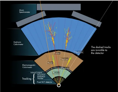
The structure of ATLAS’s detector is presented in Figure 1.3. It is built with a cylin-drical symmetry around the beam pipe axis centered on the interaction point, in order to guarantee a large acceptance in pseudorapidity (η). Ideally, it can be divided into four main regions: a barrel region, that covers low η phenomena; two end cap regions, with medium η; finally, two forward regions to cover the area with higher η. The over-all detector is therefore made up of different groups of sub-detectors, designed to track proton-proton collisions and study the particles that come out from this system. As shown in Figure 1.3 the innermost of these sub-detector systems is called Pixel Detec-tor; proceeding outwards calorimeters and muon spectrometers can be found. For what
Figure 1.3: ATLAS detector overview.
concerns the magnetic field, a central solenoid surrounds the Inner Detector in order to provide a 2 T magnetic field, while being surrounded by toroids in barrel and end-caps sections of the muon spectrometer, providing magnetic fields of approximately 0.5 T and 1 T respectively. Particles produced from collisions of protons pass firstly through the Inner Detector, which covers the region with |η| < 2.5. The charged particles will interact with different layers of the detector and produce hits, which will be used to reconstruct their trajectory. The momenta and the charge of these particles can be measured, as their trajectories are bent by a 2 T magnetic field provided by the central solenoid. A global section view of ATLAS detector is provided in Figure 1.4, illustrating how and where different particles can interact. As the innermost layer of ATLAS, the Pixel Detector provides essential informations, such as the recognition of first and sec-ond vertices. Therefore, the Inner Detector is designed to have high granularity and high momentum measurement resolution. In order to achieve the performance requirements, semiconductor detectors are used for precise measurements close to the beam (Pixel De-tector and Semiconductor Tracker ), while a noble gas deDe-tector is used in the outer layer (Transition Radiation Tracker ). Moving away from the collision point, the calorimeters
Figure 1.4: Section view of ATLAS detector in the transverse plane, illustrating layers’ positioning.
can be found. They are composed of the hadronic calorimeters and the electromagnetic calorimeters, which are designed to detect hadrons or electron/photons respectively, as well as to measure their energy and coordinates. The incident particles can interact with the instrumentation via electromagnetic or strong process, producing so a shower of secondary particles.
The calorimeters will not stop muons, as they interact very little with the calorime-ter absorber: therefore, the oucalorime-termost layer of ATLAS, named Muon Spectromecalorime-ter, is specifically designed to record and identify muons. Muons’ spectrometer is made up of four different types of chambers: two types are intended to provide position and mo-mentum measurement, while the other two types are meant to grant precise and robust information for the hardware-based trigger decision making.
1.4.1
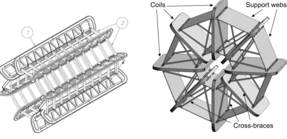
Magnetic system
The ATLAS superconducting magnet system is shown in Figure 1.5.It is made up of a central solenoid, which provides magnetic field for the Inner Detector, surrounded by a system of three large air-core toroids, generating the magnetic field for the muon spec-trometer. The overall dimensions of the magnetic system are 26 m in length and 20 m in diameter. At each end of the barrel toroid are inserted two end-cap toroids and lined up with the central solenoid. They have a length of 5 m, an outer diameter of 10.7 m and
(a) Barrel toroid magnets for ATLAS. (b) End-Cap toroids magnets for ATLAS.
Figure 1.5: Magnets system for ATLAS.
an inner bore of 1.65 m. The central solenoid extends over a length of 5.3 m and has a bore of 2.4 m. The unusual configuration of this magnetic system made its construction a real challenge, requiring a precise study and careful engineering. The Central Solenoid provides a central field of 2 T with a peak magnetic field of 2.6 T at the superconductor itself. The peak magnetic field on the superconductors in the Barrel Toroid and in the End-Cap Toroid are 3.9 T and 4.1 T respectively.
The position of the Central Solenoid in front of the calorimeter requires a careful mini-mization of the material in order to achieve the desired calorimeter performances. As a consequence, the Central Solenoid and the Liquid Argon calorimeters share one common vacuum vessel, thereby eliminating two vacuum walls.
1.4.2
Inner Detector
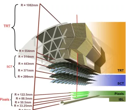
The Inner Detector (ID) is the closest detector to the beam pipe, therefore its design has to feature an excellent radiation hardness and a long term stability, while ensuring an adequate performance. As shown in Figure 1.6, the full Inner Detector is a cylinder
Figure 1.6: A section view of the ATLAS Inner Detector
with a length of 6.2 m and a diameter of 2.1 m. It covers the area with |η| < 2.5 and is segmented into cylindrical layers in the barrel region, while it has coaxial disks in the end-cap regions. As shown in Figure 1.7, ID is made up of three main different layers, which will be explained in the following paragraphs.
Transition Radiation Tracker
The Transition Radiation Tracker (TRT) detector is made up of thin drift tubes in the outer part of the ID, in which operates a non-flammable gas mixture composed by 70% Xe, 20% CO2 and 10% CF4, with a total volume of 3 m3. These straws are placed along
the pipe direction in the barrel region, while those in the end-cap region, have a radial direction.
Transition radiation is a form of electromagnetic radiation emitted when charged particle pass through an inhomogeneous mean, such as a boundary between two different means. The TRT occupies the largest space of the ID and provides the majority of the hits per track, hence highly contributing to the momentum measurement. TRT offers more hits per track in order to retrieve the information about momentum, even though it has a
Figure 1.7: Structure and arrangement of the layers of Inner Detector in the barrel region.
lower precision compared to the silicon detectors. Unlike all other active parts of ID, the drift tubes do not need to be cooled and are not subject of radiation degradation, as the gas can simply be replaced.
Semiconductor Tracker
The SemiConductor Tracker (SCT) is a tracker made up of silicon strips, with a technol-ogy similar to the one employed in the Silicon Pixel detector. The reason for using such trackers, instead of pixels, are mainly economical, since the barrel of SCT covers more than 30 times the surface of Pixel detector (63 m2 versus 1.73 m2). The barrel part of the detector is made of 4 layers, while for the end-cap 9 layers for each side have been mounted.
Pixel Detector
The last and innermost detector is Pixel Detector, which is the most important. In order to have good vertex performance, this detector has been designed to have the finest granularity. The system actually consists of four cylindrical layers, named as the
following, going outwards: Insertable B-Layer, B-Layer, Layer 1 and Layer 2. In the next section it will be described in details.
1.5
Structure of Pixel Detector
The current configuration of Pixel Detector consists of four layers, as shown in the bottom of Figure 1.7. The three outer barrels, named B-Layer(L0), Layer 1 (L1) and Layer 2 (L2), were the first to be mounted, while the Insertable B-Layer (IBL), was the last, during 2013 LHC shutdown. Together, the L0, L1, L2 layers are composed by 112 long staves in total, each one being composed by 13 modules tilted on the z axis, by 1.1◦ towards the interaction point; furthermore, in order to allow overlapping, the staves are tilted by 20◦ on the x-y plane.
A module consists of many components, such sensors, 16 Front End (FE-I3) chips, a flex-hybrid, a Module Controller Chip (MCC) and a pigtail. FE-I3s are responsible for reading the charge signal from pixels. Each FE-I3 is 195µm thick, with a top surface of 1.09cm by 0.74cm, counting 3.5 millions of transistors in 250nm CMOS technology. The module collects signals from the sensors, packaging them in a single data event, which is sent to the ROD board.
1.5.1
IBL
The Insertable Barrel Layer is a new pixel detector that has been inserted with a new shrunk beam-pipe inside the actual B-Layer. The reasons that led to this upgrade in 2013 shutdown are described hereafter.
Firstly, the inner layer was suffering a great mortality of pixels that would have increased over time, due to radiation exposure. This inefficiency caused a serious loss of b-tagging capability, which was completely restored thanks to IBL, even in the unfortunate event of B-Layer complete failure. Secondly, luminosity increase before the HL-LHC completion was too much for the read-out system and the pile-up would have led to readout ineffi-ciencies. The higher occupancy induced by luminosity would have affected the B-Layer more than the other ones, leading to inefficiencies in b-tagging [4]. Thanks to IBL, the b-tagging capability was completely restored and some redundancy was added as well; furthermore, the high granularity led to lower occupancy and higher precision. Finally,
the tracking precision was strongly improved, thanks to IBL’s pixels being closer to the interaction point. Improving the precision of impact parameters also resulted in a better sensitivity for signals in physics channels involving b-jets.
Being this close to the beam pipe forces some constraints that are not needed in other layers: electronics has to be much more radiation hard and the sensible area needs to cover more than the 70% of the surface, as in B-Layer. To achieve those objectives the FE-I4 was developed, leading to an active area of 90%.
Sensors for IBL
IBL’s sensors are different from ATLAS’s ones because of the technology chosen for the pixels. There were two main candidates:
• planar;
• 3D.
The main characteristics of these two technologies are explained hereafter, as well as the upgrade from FE-I3 chip to FE-I4.
Planar sensors were used in the B-Layer too, but the request on IBL’s ones was much stricter: in fact, the inactive border had to pass from the older 1mm to the new 450µm. Various studies were performed since B-Layer pixel were produced and now it is known that an irradiated sensor can collect much more charge if it is less thick. 3-D sensors have a completely different geometry from planar ones and are read from two electrodes at once, since the charge collected by these pixels is low. Another downside of these sensors is that noise increases along with the number of electrodes and it’s even affected by their diameter. Nevertheless, full 3-D sensors’ active area extends much closer to the surface, reducing non-sensible volume. The faces of 3-D sensors, independently from the type, are much closer one another, allowing a much lower bias voltage (150V versus 1000V of a planar sensor). This also leads to a lower leakage current and thus less cooling. When a particle passes through the electrode area, efficiency results diminished by 3.3%. This effect affects only in perpendicular particles and thus will not affect IBL for its sensors are tilted by 20◦.
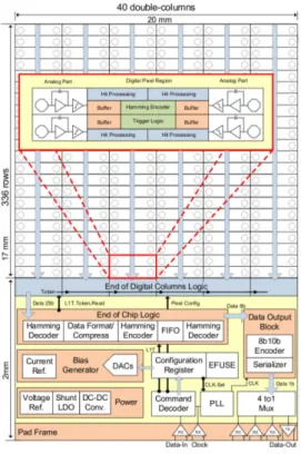
FE-I4
FE-I4, shown in Figure 1.8 is the new ATLAS pixel chip developed to be used in upgraded luminosity environments, in the framework of the Insertable BLayer (IBL) project but also for the outer pixel layers of Super-LHC.
Figure 1.8: FE-I4 Layout
FE-I4 is designed in a 130 nm CMOS process, in an 8 metal option with 2 thick aluminium top layers for enhanced power routing. Particular care has been taken to separate analog and digital power nets. With the thinning down of the gate oxide, the 130 nm CMOS process shows an increased radiation tolerance with respect to previous larger feature size processes.
The motivations for the redesign of the pixel Front-End FE-I3 came from several aspects, related to system issues and physics performances of the pixel detector. With a smaller innermost layer radius for the IBL project and an increased luminosity, the hit rate increases to levels which the FE-I3 architecture is not capable of handling.
In particular, it was shown that the current FE-I3 column-drain architecture scales badly with high hit rates and increased FE area, leading to unacceptable inefficiencies for the
IBL. FE-I4 stores hits locally to avoid a column-drain based transfer. The FE-I4 pixel size is also reduced, from 50 × 400µm2 to 50 × 250µm2 which reduces the pixel cross-section and enhances the single point resolution in z direction. FE-I4 is built up from an array of 80 by 336 pixels, each pixel being subdivided into analog and digital section. The total FE-I4 active size is 20 mm (z direction) by 16.8 mm (φ direction), with about 2 mm more foreseen for periphery, leading to an active area of close to 90% of the total. The FE is now a standalone unit avoiding the extra steering of a Module Controller Chip for communication and data output. Communication and output blocks are included in the periphery of the FE. Going to a bigger FE size is beneficial with respect to active over total area ratio as well as for the building up of modules and staves. This leads to more integrated stave and barrel concepts, and as a consequence reduces the amount of material needed per detector layer. Such a reduction of material has a drastic effect on physics performance, e.g. on b-tagging efficiency vs. light quark rejection factor. One of the main advantages of having a big FE is also the cost reduction.
Chapter 2
Off detector electronics
Before explaining the reasons that led to the development of a new board, it is wiser to look at the current set-up of the off-detector electronics for the Insertable Barrel Layer. High-energy physics experiments usually distinguish between on-detector and off-detector electronics: the former refers to the front-end electronics implemented near the detector itself, where radiation resistance is a fundamental parameter for the electronics; the latter refers to the readout system that is implemented far from the detector, thereby removing the requirement of radiation resistance and allowing the employment of more powerful devices.
The following section will present the off-detector electronics topic into details, in order to give a precise environment for which the new Pixel-ROD board was conceived and to understand the requirements that it needs to fulfill.
2.1
IBL’s electronics
The readout system for IBL requires an appropriate off-detector apparatus, which is schematically shown hereafter, in Figure 2.1. This readout system is made of several components:
• Back of Crate (BOC) board:
– Optical modules to interface FE-I4 chips with BOC board;
Figure 2.1: Schematic block view of th IBL readout system.
• Read Out Driver (ROD) board:
– Gigabit Ethernet to send front-end calibration’s histograms. • VME Crate;
• TTC Interface Module (TIM); • Single Board Computer (SBC).
Each BOC-ROD pair is able to interface and route data coming from 16 IBL modules (32 FE-I4 chips, for a total input bandwidth of 5.12 Gb/s), meaning that the whole IBL readout requires 15 BOC-ROD pairs, that can be all placed in a single VME crate.
Figure 2.2: Complete visual layout of the data acquisition system. In red the normal data path, in blue the deviation of the Histogram data path from the normal one.
A fraction of this set-up is implemented here in Bologna as well, where a VME crate hosts and in-terfaces a few BOC boards with RODs; furthermore, few front-end chips are available as well, even though the opti-cal links are missing, mainly because of their cost. The data path is presented in
sup-porting 160 Mb/s, connected to the BOC board via optical links. Here the signal from each line is converted from optical to electrical, then demultiplexed to one 12-bit-wide bus, which proceeds towards the ROD board, through the VME backplane connector. The ROD board begins the real data formatting, to build up a ROD data frame, that is sent to the TDAQ computers. On the ROD board, data can take two different paths (see Figure 2.2): the first routes the ROD data events back to the BOC, where four S-Link modules process the data towards the ATLAS TDAQ PCs, implementing a total output bandwidth of 5.12 Gb/s; the second route for data is toward the PC for histogram making, exclusively used during calibration runs in order to properly calibrate the FE-I4 chips.
2.1.1
IBL BOC
The BOC board, shown in Figure 2.3, is responsible for handling the control interface to the detector, as well as the data interface from the detector itself. Also, one major
Figure 2.3: IBL BOC board
task of the BOC is to provide the clock to the front end chips connected. In order to do so, the clock is received by the BOC from the TIM and can be delayed, if needed.
Furthermore, a Phase Locked Loop (PLL) generates copies of this clock for the ROD and the detector. The detector clock is then handled by the FPGAs and coded into the control streams for the individual detector modules.
The IBL BOC contains three Xilinx Spartan FPGAs: • one BOC Control FPGA (BCF);
• two BOC Main FPGAs (BMF).
BOC Control FPGA
The BOC Control FPGA, as the name suggests, is responsible for controlling the FPGA. A Microblaze embedded processor is instantiated on this FPGA, mainly in order to manage the Ethernet connection for the board, but it is able to implement some self test for the board as well. The BCF is also responsible for FPGAs configuration, where a two-step start-up sequence is used. Firstly, the BCF loads its configuration in “Master Serial Peripheral Interface” mode from a 64 Mbit SPI FLASH. Subsequently, the BCF firmware reads the configuration data for the two main FPGAs from a second SPI FLASH and downloads it via the Slave Serial configuration ports. Depending on the configuration, the BCF can also load software from a third SPI FLASH.
BOC Main FPGA
The two BMFs are responsible for encoding the configuration data for FE-I4 front end chips, which are coming from the ROD, into a 40 Mb/s serial stream that is sent straight to the FE-I4. This configuration stream itself can be generated by the BMFs, mainly for testing purposes. This two FPGAs also manage the deserialization of the incoming data from front-end chips on the RX path; after the data collection and the word alignment, the decoded data are sent to the ROD board. On the TX side, these two Spartan FPGAs also manage the optical connection via four S-Links to the ATLAS TDAQ system.
2.1.2
IBL ROD
The Insertable Barrel Layer Read Out Driver (IBL ROD) [5] is a board meant to be the upgrade of the older ATLAS Silicon Read Out Driver (SiROD), that is used for the ATLAS Off-Detector electronics sub-system in order to interface with Silicon Tracker
(SCT) and Pixel B0, L1 and L2 Front End Detector modules.
This board is designed in order to accomplish some tasks, like propagating timing and trigger signals to the front-end electronics, as well as sending an appropriate configuration to them. Indeed, the most important task for the ROD is accomplished during physical runs, when the board receives data and event fragments from the 32 FE-I4 chips and transform them into a ROD data frame, which is sent back to the ATLAS TDAQ, through the BOC’s S-Link connections (see Figure 2.2).
Figure 2.4: The IBL ROD board
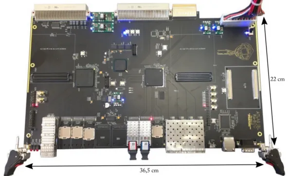
The IBL ROD (shown in Figure 2.4) is a 14-layers PCB on with many components, hereafter reported:
• One Digital Signal Processor MDSP (Texas Instruments TMS320C6201 - GJC200), which is currently not used;
• One ROD Controller (Master) FPGA (Xilinx Virtex-5 XC5VFX70T-FF1136);
• Two “Slave” FPGAs (Xilinx Spartan-6 XC6SLX150-FGG900);
• One Phase-Locked Loop PLL (Lattice ispClock 5620);
• 32 MByte SDRAM DDR;
• Four Mbit FLASH SST39VF040-70-4C-NH;
• Two GByte DDR2 SODIMM;
• 64 Mbit FLASH Atmel AT45DB642D;
• Three Gbit Ethernet interfaces with PHY DP83865.
Hereafter the main devices of the ROD board are described, in order to present the tasks and functionalities of each of them.
ROD Master
The Virtex-5 FPGA is the Master of the Read Out Driver, which must interface with the front-end chips, the triggers that come from TTC Module and all the information that refers to the Trigger itself. This FPGA contains a PowerPC, an embedded hard processor with its specific architecture. The tasks of this FPGA are many, like processing the trigger information and deliver it to the Spartan FPGAs or sending the event information (Event ID, Trigger Type and Bunch Crossing ID) to both Spartan FPGAs, so that they can be written in the header of the ROD event.
ROD Slaves
Both Spartan-6 FPGAs work as slaves on the ROD board and implement an embedded soft processor, named Microblaze, with its specific architecture. All data generated by IBL during ATLAS experiments pass through these two FPGAs and are collected inside the SSRAM; moreover, during calibration runs histograms can be generated and sent to the histogram server. Furthermore, each Spartan manages its Ethernet connection, through which histogram can be sent, as stated above.
Lattice PLL
Lattice ispClock 5620 Phase-Locked Loop (PLL) is an integrated circuit, that generates an output clock with a fixed frequency and phase relationship with the input clock. The function of the PLL is to compare the distributed clock to the incoming reference clock and change the phase and frequency of its output until the reference and feedback clocks are matched in phase and frequency. For what concerns clock sources, this board receives the clock (with a frequency of 40 MHz) from the BOC during standard runs; indeed, the need to test the ROD in a standalone mode required an internal quartz clock generator on the board. It is possible to choose between these two different clock sources by controlling a dedicated DIP switch. After that, the PLL multiplies the 40 MHz input clock, generating one with a frequency of 100 MHz. The 100 MHz and the 40 MHz clocks are then distributed all over the board.
2.1.3
TIM
The TTC (Timing, Trigger and Control) Interface Module (TIM) interfaces the ATLAS Level-1 Trigger system signals to the pixel Read-Out Drivers using the LHC-standard TTC and Busy system. This board is designed to propagate the TTC clock all over the experiment: for what concerns the IBL off-detector electronics, the TIM sends the clock to the BOC board, which then propagates it to the ROD, as stated above. Furthermore, the TIM receives and propagates triggers through the custom backplane (P3 connector).
2.1.4
SBC
The Single Board Computer, as the name suggests, is actually a computer mounted on a 6U board with a VME interface chip. It is used to control all the VME operations on the ROD and it can actually program the ROD FPGAs, usually after power up. It can also be used to monitor the temperature, or voltages, on the RODs master device.
2.2
The road towards Pixel-ROD
Since the ROD board described in the previous section met all the expectations that ATLAS experiment had, it was decided to implement this system also for all other layers
(B0, L1, L2). The effort on the IBL electronics required 15 ROD boards to be produced and tested in 2014, while the remaining layers required about 110 boards, whose last batch has just been installed at ATLAS. Alongside with this work, a huge effort was also spent into the development and upgrade of the firmware for the ROD boards.
The knowledge acquired with IBL electronics made also clear the limits of this system, especially looking to the future upgrade of the whole LHC detector to the higher lumi-nosity HL-LHC. The established Long Shutdown in 2023 [6] for the upgrade of the whole LHC will bring the nominal luminosity from five to seven times the actual one, with an expected luminosity peak of Lpeak = 7.5 × 1034cm−2s−1. Such huge improvement in
luminosity also means that the electronics will need to withstand a much higher data rate.
Looking into this direction, many electronic boards have been presented for the read-out of such experiments [7]. All the available electronic board’s projects share a common feature: the implementation of an electronic board designed to be flexible and highly con-figurable, with PCIe interface, as well as powerful FPGAs connecting to many optical transceivers.
Looking into high-speed devices, we decided to keep working with FPGAs from Xilinx, upgrading to the 7-Series family. This decision was taken in order not to waste all the experience and the efforts spent on the ROD board, while allowing the portability of the firmware onto this new one, named Pixel-ROD, after upgrading it on the newly introduced platform. Furthermore, given the success of the Master-Slave architecture from the ROD board, as well as for the reason just explained above, it was decided to use two FPGAs on the Pixel-ROD board. Since the process of creating and debugging such highly complex boards often turns out to be very time consuming, it was decided to design the Pixel-ROD from two evaluation boards made by Xilinx: the KC705 and the ZC702.
2.2.1
KC705
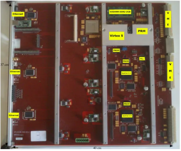
For the slave device we looked for a powerful FPGA from Xilinx’s Kintex family, a good example of which was already given by a Xilinx’s evaluation board, named KC705. The KC705, shown in Figure 2.5, was an interesting board for us in many ways, whose main devices and features are listed below [8]:
Figure 2.5: Xilinx’s KC705 demo board
• Kintex-7 28nm FPGA (XC7K325T-2FFG900C); • 1GB DDR3 memory SODIMM;
• PCI Express Gen2 8-lane endpoint connectivity; • SFP+ connector;
• Two VITA 57.1 FMC Connectors (one HPC, one LPC);
• 10/100/1000 tri-speed Ethernet with Marvell Alaska 88E1111 PHY; • 128 MB Linear Byte Peripheral Interface (BPI) flash memory; • 128 Mb Quad Serial Peripheral Interface (SPI) flash memory; • USB-to-UART bridge;
• USB JTAG via Digilent module; • Fixed 200 MHz LVDS oscillator; • I2C programmable LVDS oscillator;
First of all, the KC705 is a PCIe board: this interface is very important for newly developed boards, since it is the one that is more likely to replace the role of slower VME buses. In fact, VME bus data rate is 200 MB/s, while an 8 lanes PCIe Gen2 bus supports a data rate of 4GB/s. Furthermore, PCIe allows a new possible installation configuration: one or two of these boards can be directly connected on the motherboard of TDAQ PCs, thereby giving straight access to the main resources of the PC, like CPU and RAM, for a faster response and providing also an easier installation. This configuration is the one towards which ATLAS, as well as other experiments like CMS, are aiming to for the experimental phase that will start after the Long Shutdown in 2023.
Kintex-7 FPGA
The new Kintex-7 is a powerful medium-range FPGA, that can easily fulfill the role of both Spartan-6 devices on the ROD board [9, 10].
The Xilinx Kintex-7 XC7K325T-2FFG900 on this board has the following features:
• Advanced high-performance FPGA logic based on real 6-input lookup table (LUT) technology configurable as distributed memory;
• High-performance DDR3 interface supporting up to 1866 Mb/s;
• High-speed serial connectivity with built-in 16 gigabit transceivers (GTX) from 600 Mb/s to maximum rates of 12.5 Gb/s, offering a special low-power mode, optimized for chip-to-chip interfaces;
• A user configurable analog interface (XADC), incorporating dual 12-bit analog-to-digital converters (ADC) with on-chip temperature and supply sensors;
• Powerful clock management tiles (CMT), combining phase-locked loop (PLL) and mixed-mode clock manager (MMCM) blocks for high precision and low jitter;
• Integrated block for PCI Express (PCIe), for up to x8 Gen2 Endpoint and Root Port designs;
Kintex-7 (Pixel-ROD) Spartan-6 (ROD) Logic cells 326080 147443
BRAM Blocks (18 Kb) 890 268
Memory Interface 1866 Mb/s 800 Mb/s Table 2.1: Brief comparison between Spartan-6 and Kintex-7 features.
VITA 57.1 FMC connectors
Another strong point of this board are its two VITA 57.1 FMC [11] connectors, that allow to interface many external devices, thanks to this particular and standardized connection, shown in Figure 2.6. This additional I/O connection is achieved thanks to external I/O
Figure 2.6: A Xilinx demo board displayed as carrier, with external FMC mezzanine.
mezzanine module. In this standard, the board carrying the FPGA acts as carrier for the FMC mezzanine module, which enables the board to have flexible and different external connections. This connector standard supports up to 10 Gb/s transmission with adaptive equalized I/O, as well as single ended and differential signalling up to 2 Gb/s.
Two types of FMC connectors exist, both of which are present in the KC705 board (see Figure 2.5):
• Low Pin Count (LPC) connector, providing 68 user-defined single-ended signals or 34 user-defined differential pairs, one transceiver pair, one GTX clock and one differential clock (160 total pins);
• High Pin Count (HPC) connector, providing 160 user-defined single-ended signals (or 80 user-defined differential pairs), 10 serial transceiver pairs, two GTX clocks, four differential clocks (400 total pins).
On the KC705 four GTX transceivers are wired to the FMC HPC connector, while only one is connected to the FMC LPC. Therefore these connectors allow a new level of flexibility for FPGA boards, granting the user the possibility to properly choose its I/O devices by changing mezzanine module. Furthermore, this standard eliminates the need for complex protocol logic on the mezzanine, since devices placed there can be connected to the main board JTAG and I2C chains, therefore allowing a lower complexity of FPGA design and a simpler debug.
PCI Express connector
Since the Kintex-7 FPGA on KC705 board supports a PCIe connection up to Gen2 x8, the 8-lane PCI Express [12] edge connector performs data transfers at the rate of 5 GT/s. The PCIe transmit and receive signal traces have a characteristic impedance of 85Ω ±10%. The PCIe clock is routed as a 100Ω differential pair.
2.2.2
ZC702
The second demo board we took inspiration from is the Xilinx’s ZC702, shown in Fig-ure 2.7. As previously described, the ROD board hosts a Virtex-5 FPGA, implementing an embedded hard processor named PowerPC. This feature is highly important on the master FPGA, since it allows to write software (using C or C++ language), that can be run on this processor. For this reason the ZC702 becomes interesting for our project, since its FPGA embeds a hard processor [13], which allows to avoid changes in the firmware each time a particular function needs to be tested.
Hereafter the main features of the ZC702 demo board are listed:
• Zynq 7000 FPGA (XC7Z020-1CLG484C), featuring two ARM Cortex-A9 MPCore hard processors;
Figure 2.7: Top view of ZC702 demo board
• 1 GB DDR3 component memory (Micron MT41J256M8HX-15E); • 10/100/1000 tri-speed Ethernet with Marvell Alaska 88E1116R PHY; • 128 Mb Quad SPI flash memory;
• USB-to-UART bridge;
• USB JTAG interface using a Digilent module; • Two VITA 57.1 FMC LPC connectors;
• Fixed 200 MHz LVDS oscillator;
Zynq-7000 FPGA
The Zynq 7000 FPGA consists of an integrated Processor System (PS) and Programmable Logic (PL). The PS integrates two ARM CortexR TM-A9 MPCoreTM with a frequency
and peripherals including USB, Ethernet, SPI, SD/SDIO, I2C, CAN, UART, and GPIO. The PS runs independently of the PL and boots at power-up or reset.
Even though a detailed description of the architecture of the Zynq is not in the intention of this thesis, it necessary to proceed with a brief explanation of this system, in order to provide a better understanding of the topics covered in the next chapter. A schematic diagram of the Zynq FPGA is given in Figure 2.8, which illustrates the functional blocks. The Processor System is surrounded by a blue line in Figure 2.8,
Figure 2.8: Zynq 7000 architecture overview
while the Programmable Logic by a yellow line. The PL part is structured just as any other FPGA, featuring 85K logic cells and 560 KB of Block RAM, making it equivalent to an Artix -7 FPGA from the Xilinx 7 Series family.R
Indeed, the Processor System is far more complex, as figure Figure 2.8 shows. It can be divided in four main functional blocks:
• Memory interfaces; • I/O peripherals (IOP); • Central interconnect.
APU The Application Processor Unit [14], shown in Figure 2.9, is mainly made up of two ARM processing cores, each one with its associated computational units: a NEON Media Processing Engine (MPE) and Floating Point Unit (FPU), a Memory Management Unit (MMU) and a Level 1 cache memory, splitted in two sections for instructions and data.
Figure 2.9: Simplified block diagram of the Application Processing Unit
The APU also contains a Level 2 cache memory, and a further On Chip Memory (OCM). Finally, a Snoop Control Unit (SCU) forms a bridge between the ARM cores and the Level 2 cache and OCM memories.
The ARM Cortex-A9 processor mount-ed on this demo board can be clockmount-ed up to 667 MHz. Each of the two cores has separate Level 1 caches for data and instructions, both of which are 32 KB; as in the general case, this permits local
storage of frequently required data and instructions for fast access times and optimal processor performance.The two cores additionally share a larger Level 2 cache of 512 KB for instructions and data, and there is a further 256 KB of on-chip memory within the APU. Since modern computing systems are always very demanding for what concerns memory requirements, it often happens that the finite amount of memory available is not enough. In this respect, virtual memory can prove to be very useful, as it makes appear as there is more memory available in the system than what actually is. Here is where the Memory Management Unit (MMU) becomes helpful, since its role is to translate between physical and virtual addresses.
The Snoop Control Unit (SCU) undertakes several tasks, involving the interface between the processor and Level 1 and 2 cache memories and is mainly responsible for
maintain-ing memory coherency between the processor data cache memories, which are marked as L1(D) in Figure 2.9, and the shared Level 2 cache memory. It also initiates and con-trols access to the Level 2 cache, arbitrating between requests from the two cores where necessary.
From a programming perspective, support for ARM instructions is provided via the Xilinx Software Development Kit (SDK) which includes all necessary components to de-velop software for deployment on the ARM processor, as it will be shown more accurately in the next chapter.
Finally, one last additional functionality to the main ARM processor is the NEON engine, which provides Single Instruction Multiple Data (SIMD) facility to enable accel-eration of DSP type algorithms. NEON instructions are an extension to the standard ARM instruction set, and can either be used explicitly, or by ensuring that the C code follows an expected form and thus allows NEON operations to be inferred by the com-piler. As the SIMD term suggests, the NEON engine can accept multiple sets of input vectors, upon which the same operation is performed simultaneously to provide a cor-responding set of output vectors. This style of computation is suitable for applications involving digital signal processing (DSP), which operate on a large number of data sam-ples simultaneously with algorithms that are inherently parallel.
Memory interfaces The Zynq has two main memory interfaces, which connect it to few different memory types. Through the Central Interconnect, the APU can access the controllers of QSPI and other built in memories. However, the APU can access another very important memory controller, which is the DDR memory controller.
The DDR memory controller supports DDR2, DDR3, DDR3L, and LPDDR2 [15] devices and consists of three major blocks: an AXI memory port interface (DDRI), a core con-troller with transaction scheduler (DDRC) and a concon-troller with digital PHY (DDRP). The DDR interface (DDRI) arbitrates the requests from the eight ports (four reads and four writes). The arbiter selects a request and passes it to the DDR controller and trans-action scheduler (DDRC). The arbitration is based on a combination of how long the request has been waiting, the urgency of the request, and if the request is within the same page as the previous request. The DDRC receives requests from the DDRI through a single interface. Both reads and writes flow through this interface. Read requests include a tag field that is returned with the data from the DDR. The PHY processes read/write
requests from the controller and translates them into specific signals within the timing constraints of the target DDR memory. Signals from the controller are used by the PHY to produce internal signals that connect to the pins via the digital PHYs. The DDR pins connect directly to the DDR devices via the PCB signal traces. The DDR controller PHY (DDRP) drives the DDR transactions.
I/O Peripherals The I/O peripherals (IOP) are a collection of industry-standard in-terfaces for external data communication. The Zynq PS features a variety of inin-terfaces, which can be ideally divided into 2 groups: PS-PL interfaces and PS to External Compo-nents interfaces. The latter and most important group of interfaces is shown on the left side of Figure 2.8, where connection between the PS and external interfaces is achieved primarily via the Multiplexed Input/Output (MIO), that provides 54 pins of flexible connectivity, meaning that the mapping between peripherals and pins can be defined as required. Certain connections can also be made via the Extended MIO (EMIO), which is not a direct path from the PS to external connections, but instead passes through and shares the I/O resources of the PL. The available I/O includes standard communications interfaces, like Gigabit Ethernet Controllers, USB Controllers, UART Controllers and General Purpose Input/Output (GPIO), which can be used for a variety of purposes, including simple buttons, switches, and LEDs.
Interconnects The interconnects that are located within the PS are designed to work as switches with the specific task to facilitate the communication of read, write and response transactions between master and slave client. There are many interconnects within the Zynq PS, as shown in Figure 2.8: the most important one is the Central Interconnect, which interfaces many peripherals with the APU, therefore allowing the latter to send data as well as register configuration for the I/O peripheral interfaces. Other interconnects can be seen in Figure 2.8, such as PL to Memory Interconnect or OCM Interconnect, all sharing the same task, that is to allow communication exclusively from the permitted masters to specific slaves, via AXI protocol communication.
2.3
The Pixel-ROD board
The analysis of the two demo boards, described in the previous section, was fundamental for the realization of the new Pixel-ROD board. Coming this far, we decided to design the Pixel-ROD as a fusion from both KC705 and ZC702. While creating Pixel-ROD by merging the two demo boards, many features had to be removed, since not useful for a readout board, as we wanted the Pixel-ROD to be. Furthermore, other features had to be re-designed, as they needed to be shared among the whole hardware of the new board.
Speaking about KC705, with reference to the Figure 2.5, the main features that had been removed were of course the LCD display, the SD card reader and the HDMI port, as well as a few GPIO buttons and LEDs. On the side of ZC702, almost the same features were removed: SD card reader, HDMI port, GPIO buttons and LEDs were removed, along with one of the two LPC FMC, the USB port and PMODS connectors. All these features removed made room to more useful ones, like buses between FPGAs, which are mandatory since they are needed to implement a ROD-like "Master-Slave" architecture. Therefore, principal devices and features that are implemented on the Pixel-ROD board are the following:
• Kintex-7 28nm FPGA (XC7K325T-2FFG900C);
• Zynq 7000 FPGA (XC7Z020-1CLG484C), featuring two ARM Cortex-A9 MPCore; • 2 GB DDR3 memory SODIMM (Kintex DDR);
• 1 GB DDR3 component memory (Micron MT41J256M8HX-15E, Zynq DDR3); • PCI Express Gen2 8-lane endpoint connectivity;
• SFP+ connector;
• Three VITA 57.1 FMC Connectors (one HPC, two LPC); • Two 10/100/1000 tri-speed Ethernet with Marvell Alaska PHY; • Two 128 Mb Quad SPI flash memory;
• USB JTAG interface (using a Digilent module or header connection); • Two fixed 200 MHz LVDS oscillators;
• I2C programmable LVDS oscillator;
As previously stated, on the Pixel-ROD a bus has been added between the two FPGAs in order to obtain the necessary communication. There are three main types of buses, each one intended to provide specific features: the first and most important type of connection is given by the 21-bit differential bus, intended to provide an high speed communication link between Kintex and Zynq; the second type of bus is a 1-bit differential line whose main task is to share a common clock between the two FPGAs, whenever is needed; the last type of interconnection bus is a 5-bit wide, single ended bus, which is a general purpose bus. Along with these features that have been newly introduced, others had to
Figure 2.10: Custom JTAG configuration header. The blue lines and circles highlight the full JTAG chain configuration, while in red it is highlighted the one activating the internal JTAG, excluding the Kintex from the global chain.
be tuned to fulfill their roles, like JTAG chain and power supply stage. The former has been modified in order to include the main devices on the board, which are of course both FPGAs and two out of three FMC connectors (those controlled by Kintex). The JTAG chain was modified also in another way: a 12 (3x4) pin header (see Figure 2.10) was added in order to allow the possibility to exclude the Kintex from the JTAG chain. This
feature was added with the idea of prevent unwanted programming of the slave FPGA. Furthermore, an internal JTAG from Zynq to Kintex has been added: this feature allows to program the slave FPGA with the desired firmware, using Zynq as Master, once its firmware is defined. This can be very helpful during debugging session, when the Pixel-ROD board can be installed inside a PC, where it can be difficult to access to a JTAG port.
The last feature that had to be re-invented while designing Pixel-ROD board is the power supply stage. Coming from the two demo boards, which have the same devices for the power supply stage, we decided not to barely copy it, but to try to merge them instead. The reason behind this decision is mainly one: since the Pixel-ROD is intended to fit into a PC case [16], replying both supply stages would have been faster, but would have compromised the possibility to insert the board in a PC case for space related reasons. In Figure 2.11 it is shown a schematic representation of both demo boards power supply stage. As the figures show, they are very similar, since they both take in 12V from a Molex connector and provide this to different power controllers. These power controllers cover a very important role, since they do not only obtain from the 12 V input the desired output voltages, but they provide the precise sequence of power up. With the growth in FPGA complexity, the need for a precise sequence of power up began to play a very relevant role. On the Pixel-ROD board this task is achieved thanks to three Digital Pulse-Width Modulation (PWM) System Controller (UCD9248) [17], the same devices implemented on the demo boards. The UCD9248 is a 4 rail, 8 phases synchronous buck digital PWM controller designed for non-isolated DC/DC power application. When multiple power stages are configured to drive a voltage rail, the UCD9248 automatically distributes the phase of each DPWM output, in order to minimize ripple. This device integrates dedicated circuitry for DC/DC loop management with RAM and flash memory and a serial interface to support configurability, monitoring and management. In order to facilitate the configuration of these devices, a PC based Graphical User Interface (GUI), named Fusion Digital Power Designer, is provided by Texas Instrument. This tool allows to configure the system operating parameters for the application, storing the configuration to on-chip non-volatile memory. Furthermore, it is possible to get real time measurements of sensed voltages, once the device in configured and correctly interfaced.
Power Controller 1 Switching Regulator #1 VCCINT 1.0V @ 20A Dual Switching Regulator #1 VCCAUX (MGTVCCAUX) 1.8V @ 10A Dual Switching Regulator #1 VCC3V3 3.3V @ 10A Switching Regulator #2 VCCADJ 2.5V @ 10A 12V Power Controller 2 Dual Switching Regulator #2 VCC1V5 2.5V @ 10A Dual Switching Regulator #2 VCC2V5 2.5V @ 10A Dual Switching Regulator #3 MGTAVCC 1.0V @ 10A Dual Switching Regulator #3 MGTAVTT 1.2V @ 10A Linear Regulator 5.0V @ 1.5A max Linear Regulator VCCAUX_IO 1.8V or 2.0V @ 1.8A Linear Regulator VCC1V8 @ 1.8A Linear Regulator XADC_VCC 1.7V-2.0V @ 300mA Linear Regulator VCC2V8 @ 300mA
(a) KC705 power supply stage.
Power Controller 1 12V Power Controller 2 Dual Switching Regulator #3 VCCADJ 2.5V @ 10A Dual Switching Regulator #3 VCC1V5 1.5V @ 10A Dual Switching Regulator #4 VCCMIO_PS 1.8V @ 10A Dual Switching Regulator #4 VCCBRAM 1.0V @ 10A Dual Switching Regulator #1 VCCINT 1.0V @ 10A Dual Switching Regulator #1 VCCPINT 1.0V @ 10A Power Controller 3 Dual Switching Regulator #5 VCC3V3 3.3V @ 10A Dual Switching Regulator #5 VCC2V5 2.5V @ 10A Linear Regulator VTTDDR_PS 0.75V @ 3A Dual Switching Regulator #2 VCCAUX 1.8V @ 10A Dual Switching Regulator #2 VCCPAUX 1.8V @ 10A
(b) ZC702 power supply stage.
Figure 2.11: Schematic representation of demo boards power supply stage
interconnected one another, so that many different ways of sequencing the power up of the output rails are available. Of course, such complex devices need a reserved programming method: this feature is provided through the PMBUS connector, to which each device is interfaced. By connecting a PC running Fusion Digital Power Designer to the PMBUS port on the board, via its specific USB interface adapter, it is possible to configure every single parameter of the power up sequence. So after the analysis of the demo boards, the power stage for Pixel-ROD board was designed and is here reported in Figure 2.12. It is made up of three different Digital PWM System Controller (UCD9248), that are all supplied by the 12V voltage input, which is taken from Molex connector and then filtered. Each one of the UCD9248 controls four DC/DC Switching regulators, which are of three different types:
Power Controller 1 Switching Regulator #1 VCCINT 1.0V @ 20A Switching Regulator #2 VCCMIO/VCCAUX 1.8V @ 20A Switching Regulator #3 VCC3V3 3.3V @ 10A Switching Regulator #4 VCCADJ 2.5V @ 10A 12V Power Controller 2 Dual Switching Regulator #1 VCC2V5 2.5V @ 10A Dual Switching Regulator #1 VCC1V5 1.5V @ 10A Dual Switching Regulator #2 MGTAVCC 1.0V @ 10A Dual Switching Regulator #2 MGTAVTT 1.2V @ 10A Power Controller 3 Dual Switching Regulator #3 VCCAUX_IO 1.8V @ 10A Dual Switching Regulator #3 VCCBRAM 1.0V @ 10A Switching Regulator #5 MGTAVCCAUX 1.8V @ 10A Switching Regulator #6 VADJ_custom 1.0V @ 10A Linear Regulator VCC5V0 5.0V @ 2A Linear Regulator VCCSPI 2.8V @ 300mA Linear Regulator VCC1V8 1.8V @ 1.5A Two Linear Regulators VTT_DDR 0.75V
Figure 2.12: Schematic of Power Supply stage for Pixel-ROD
current of 20A;
• PTD08A010W, a single output switching regulator, with a maximum supplied current of 10A;
• PTD08D210W, a dual output switching regulator, with a maximum supplied cur-rent of 10A on each output.
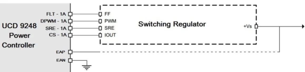
Figure 2.13: Schematic view of the interconnection between a single rail of the UCD9248 power controller and its switching regulator.
eight possible phases. In order to do so the Digital PWM System Controller needs a few signals (see Figure 2.13):
• a DPWM signal, that is the Digital Pulse Width Modulation output signal through which the switching regulator is able to define the output voltage;
• a EAP/EAN differential input signal through which the UCD9248 can read the output voltage from the DC/DC switch, therefore regulating or assessing an error whenever the read value is different from the one decided by the user;
• a CS signal, which is the Current Sense input signal, used to measure the output monitor value and eventually assess a fault if measurement is outside the user-defined range;
• a FLT signal, which is the input Fault signal used to assess an error on the actual monitored values, with respect to user-defined parameters.
2.3.1
Prototyping
From the analysis of all the required voltages and currents of the Pixel-ROD board from Figure 2.12, it is possible to determine the maximum required power from the board:
P =X
i
ViIi = 242W
This means that the board has to be realized in order to withstand a maximal input current of 20 A on the 12 V Molex connector, which is a considerable value of current
for this type of applications. The solution to this level of criticality is achieved through a good stackup.
Figure 2.14: Stackup of Pixel-ROD.
The stackup defines the composition, the thickness and the function of each layer of a Printed Circuit Board (PCB). In the Pixel-ROD case a safe stackup was adopted, which is shown in the Figure 2.14: a 16 layers PCB was chosen in order to provide the necessary space to the high number of traces in the board; furthermore, the required level of insulation is achieved by alternating signal layers with ground layers, as well as concentrating the power layers into the innermost section of the board.
Figure 2.15: Pre-Layout of Pixel-ROD
Given all these features, a layout was proposed for the Pixel-Rod board, which is represented in Figure 2.15. This proposed layout is pretty similar to the one of KC705 demo board, but with some adjustments: firstly, the SFP connector is moved on the left edge of the board, in order to shorten the length of the traces that connect the SFP to Kintex FPGA, thus allowing the possibility to reach a nominal speed of 9.6 Gbps; the power section has to be implemented on the right side of the boar, therefore being distant from critical devices, like DDR3 SODIMM, or again the SFP connector. Before
the fabrication of the board, a simulation was performed for the SFP connector, in order to verify the absence of major faults on this high-speed signal. By means of Hyperlinks software from Mentor Graphics, it was simulated a signal with data rate of 9.6 Gbps through the designed SFP traces and connector. The result, reported in Figure 2.16, shows what is called eye diagram: by simulating iteratively the signal over its traces, triggering on both rising and falling edges, it is possible to control the whether the periodicity of the signal is preserved or not. Many factors can damage the integrity of the signal, such as interferences with other signals or even noisy power supplies, making it shift or stretch between different cycles. These factors cause the shrinking of the blank area between signal’s levels (named eye), therefore deteriorating the signal itself. In Figure 2.16 it is possible to notice that the eye is open, meaning that the signal is preserved, even at such high data rate.
Another constraint in the realization of the board was its size. Since the Pixel-ROD is intended to fit a PC case, as already stated above, the maximum length for the board has been set to 30 cm, thereby adding little space for the device placement. Furthermore, since the Pixel-ROD is a PCIe board, also a constraint on the thickness was added, thus fixing the maximum number of layers to 16, in order to respect the PCIe standards. Finally, the height of the board was left free, to allow sufficient room for all the devices necessary on Pixel-ROD.
The result of all these efforts are hereafter shown, in Figure 2.17.
As the figure shows, the board height has been essentially increased, providing more room for the power supply Molex, as well as for the FMC LPC connected to the Zynq. Furthermore, in order to be compliant to VITA 57.1 FMC standard, the area above the two adjacent FMC connectors has been left empty.
Two prototypes of Pixel-ROD have been produced, in order to have a faster debug and hardware wake up phase, which is the topic of discussion of the next chapter.
Figure 2.17: The Pixel-ROD prototype. The components highlighted in blue are those connected to Kintex FPGA; the red ones are linked to the Zynq FPGA. The components highlighted in yellow belong to the power stage.
Chapter 3
Pixel-ROD tests results
Complex electronic boards, such as the Pixel-ROD, need a careful testing and hardware wake-up phase, especially when just at the prototype stage. With the expression hard-ware wake-up are here intended all the actions needed to assure that, when the board is powered up for the first time, the hardware is working correctly. This first step is needed in order to prove that the hardware is capable of being correctly configured, hence providing a suitable environment where major faults of the board are excluded and the user’s firmware can be actually tested.
The work that has been done on the Pixel-ROD can be mainly divided into 2 stages: the first goal has been the correct configuration of the board power up, which passes through the configuration of all three UCD9248 power controllers; the second goal has been the validation of devices and functionalities of Pixel-ROD, by implementing tests that aim to verify the expected performances. Therefore, a detailed description of the steps stated above is hereafter reported.
At present - March 2017 - all fundamental devices have been tested on both prototype boards, with the exception of FMCs and PCIe connectors, since a specific instrumenta-tion is needed in order to verify these interfaces.
3.1
Power supply debug and test
As previously stated, when such highly complex prototypes are produced with pro-grammable power supply devices, the act of switching on the board turns out to be
a non-trivial and high risk task. Therefore, during the design phase, the board has been given a specific feature to prevent damage to sensitive devices, like the FPGAs. In order not to spread uncontrolled voltages all over the board, the power stage was sectioned from the rest of the board by means of solder pads, shown in figure Figure 3.1.
Figure 3.1: Solder pad example.
Figure 3.2: Schematic detail of mistaken connections.
Solder pads are basically interruptions between ad-jacent power planes that are expected to be con-nected during normal operations; since they bring this interruption on a reachable layer (top or bot-tom of the board), they allow the soldering of the disjointed planes by means of a drop of tin or a 0 Ω resistor.
Starting with all open solder pads, we powered up the Pixel-ROD prototype number one by means of an external power supply, while monitoring it by means of an infrared camera and limiting the in-put current to 1 A, in order to prevent major faults. As soon as we powered up the system the generator reached the current limit, hence providing us with the information that something was wrong.
The reason behind this first fault is shown in Fig-ure 3.2: a mistake during the design phase allowed both digital and analog grounds to be left floating,
due to components Z10 and Z11 being erroneously declared as Do Not Place (DNP). Luckily, this problem was quickly identified and fixed, by welding them to the general ground plane.
An almost identical problem was found on the EAN signals (see signal description in 2.3): these nets need to be referred to the ground, in order to provide a correct read value for the UCD9248. Further checks on the generated netlist (the file listing each existing trace on the board) proved that all of these nets were not actually tied to the common ground, but rather to another reference with the same name, that the designing software had created. As a result, this error was causing a misleading read of the voltage value by the power controllers. Again, this problem was solved by patching the board with an
external wire connected with the ground signal provided via Molex input connector.
Figure 3.3: Schematic detail of the overly ag-gressive power sectioning. The solder pad J 123 placed before the power output, that ex-cludes voltage feedback too.
Aside for a DC/DC switch mounted backwards and for a couple of feedback signals (EAP/EAN differential pairs) that were reversed, thereby providing feedback to the wrong rail, a couple of more sneaky issues were identified and patched. For what concerns the first one, we realized that the sectioning of power supply stage was too much aggressive: in other words, the solder pads were placed way too upstream, hence excluding not
only the sensitive devices of Pixel-ROD, but also the voltage feedbacks to the UCD9248 power controllers, as shown in Figure 3.3 with reference to Figure 3.8. This caused the controllers to be unable of correctly configure the DPWM signal, which is used to control the DC/DC output voltage. The last mistake and maybe the most tough to identify,
Figure 3.4: Schematic detail of last mistake identified.
is shown in Figure 3.4: on the left side are reported 3 signals coming from one of the three UCD9248 controllers; on the right side the same three signals from the DC/DC switching stage. It is possible to notice that these connection are switched one another, therefore implementing a mistaken connection from the DC/DC switching stage to the UCD9248. It was particularly hard to identify this issue because of the number of nets involved: from each power controller 80 nets go to the DC/DC switching stage. Fur-thermore, in the schematic design of the Pixel-ROD each power controller is described but not straightly connected to its DC/DC switches. This is due to the fact that in the making of the schematic design for these highly populated boards, a hierarchical struc-ture is used, where each device is described in a single page. In this type of schematic, a specific page usually named Top Module or just Top, is reserved to trace and sum up the connections between devices described in their specific page. The mistake shown in
Figure 3.4 had to be found in the Top Module of Pixel-ROD schematic design, among all the connection between the high number of devices that make up the board.
After this long debug period, we could finally program the three UCD9248 power controllers by means of Texas Instruments Fusion Digital Power Designer.
Figure 3.5: Schematic representation of power controllers programming setup.
PMBUS Address RP M BU S(kΩ) 11 205 10 178 9 154 8 133 7 115 6 100 5 86.6 4 75 3 64.9 2 56.2 1 48.7 0 42.2
Table 3.1: Address resistor code. A brief representation of the set-up needed to
configure these devices is reported in Figure 3.5. Firstly, a Universal Serial Bus (USB) to Power Management BUS (PMBUS) adapter is used to in-terface the PC with the Pixel-ROD’s PMBUS re-served header connector. The PMBUS connection is an open standard protocol that defines a bus for communicating with power conversion and other devices. It is based on the System Management Bus (SMBUS), which is a single-ended two-wire bus, de-rived from I2C for the purpose of lightweight
com-munication. As shown in Figure 3.5, each device present on the Pixel-ROD board has its specific ad-dress, which is hardware-coded by means of two resistors.
At power-up, the power controller applies a bias current (IBIAS = 10µA) to each address detect pin,