for microfluidics applications
Cite as: APL Mater. 7, 081108 (2019); https://doi.org/10.1063/1.5070136Submitted: 19 October 2018 . Accepted: 24 July 2019 . Published Online: 14 August 2019 Matteo Agostini , Gina Greco , and Marco Cecchini
COLLECTIONS
This paper was selected as an Editor’s Pick
ARTICLES YOU MAY BE INTERESTED IN
Research on the selective adhesion characteristics of polydimethylsiloxane layer
AIP Advances
8, 095004 (2018); https://doi.org/10.1063/1.5041867
2D nanosheet-constructed hybrid nanofillers for polymer nanocomposites with synergistic
dispersion and function
APL Materials
7, 080904 (2019); https://doi.org/10.1063/1.5110228
Enhanced stability of guanidinium-based organic-inorganic hybrid lead triiodides in
resistance switching
Polydimethylsiloxane (PDMS) irreversible
bonding to untreated plastics and metals
for microfluidics applications
Cite as: APL Mater. 7, 081108 (2019);doi: 10.1063/1.5070136
Submitted: 19 October 2018 • Accepted: 24 July 2019 • Published Online: 14 August 2019
Matteo Agostini,a) Gina Greco, and Marco Cecchini
AFFILIATIONS
Laboratorio NEST, Istituto Nanoscienze-CNR and Scuola Normale Superiore, Piazza San Silvestro 12, 56127 Pisa, Italy a)Email:[email protected]
ABSTRACT
In order to properly manipulate liquids into microfluidic networks, an accurate sealing of the device is of paramount importance. Poly-dimethylsiloxane (PDMS) is ubiquitously used for fabricating microfluidic components, owing to its low cost, easy and fast fabrication, and optical transparency. However, PDMS is characterized by low surface energy, making its bonding to many substrates not trivial. Here is presented a versatile technique for PDMS microchannel bonding on untreated plastic and metal surfaces. First, the PDMS surface is function-alized with (3-aminopropyl) triethoxysilane (APTES) for further cross-linking with epoxy groups. Then, the PDMS-APTES surface is coated with Norland Optical Adhesive 74 (NOA74). Finally, the PDMS-APTES-NOA74 is put in contact with the target material and the glue is cured under a UV light. In order to characterize the bonding strength, a complete PDMS-on-gold microfluidic device is fabricated and tested with increasing injection pressures. Different liquids and a gas (nitrogen) are applied without leakage up to 2 bars, a value comparable to the one reported for the standard glass-PDMS bonding through plasma oxygen activation. The same technique is then successfully replicated with other nonmetallic substrates of interest for microfluidics, i.e., glass, poly(methyl methacrylate), polystyrene, polyethylene terephtha-late, cyclic olefin copolymer, demonstrating its great versatility and potential for, but not limited to, microfluidic applications and LOC engineering.
© 2019 Author(s). All article content, except where otherwise noted, is licensed under a Creative Commons Attribution (CC BY) license (http://creativecommons.org/licenses/by/4.0/).https://doi.org/10.1063/1.5070136., s
Lab on chips (LOCs) are devices expected to play a major role in many fields: biology, bioengineering, chemistry, and clin-ical diagnostics among all. LOCs are unique tools able to embed and automatize on a small chip surface (mm2-cm2) many opera-tions that are usually performed by trained personnel in specialized facilities. These operations include adding/mixing reagents, manip-ulating biological materials, and performing chemical and biochem-ical analyses.1,2 This can be accomplished by exploiting micro-and nanofabrication techniques for realizing miniaturized actuators, sensors, and microchannel networks. Thanks to the characteristics of the flows at the microscale, an unprecedented precision and con-trol of the reactions is thus achieved, along with a significant volume reduction of reagents and waste.3–5
One essential aspect in a LOC is the sealing of the microfluidic components. A tight sealing is necessary to properly inject and route
liquids without leakages, avoid external and cross-contamination, and protect the sensitive areas during device operation. Yet, this is not a straightforward task. As the microchannel dimension approaches the submillimeter scale and the network complexity increases, a good conformal contact of the layout of microchannels and the substrate is necessary over a large area.6In addition, the LOC substrates and the microchannel networks can be made of different materials (e.g., glass, plastic, metal, a composition of the previous) or have different coatings. Common substrates for LOCs are, for exam-ple, glass, cyclic olefin copolymer (COC), and poly methyl methacry-late (PMMA). These substrates are used for their low-cost, optical transparency, and easiness of patterning with large-scale production processes. On the other hand, one of the most widespread materi-als for sensing and/or electrical connections purposes in LOCs is gold, owing to its resistance to oxidization, optical and electrical
different materials results in a case-by-case approach to the sealing issue.
In the last few decades, polydimethylsiloxane (PDMS) has been ubiquitously used as a material for realizing microfluidic net-works, owing to its low cost, easy and fast fabrication through soft-lithography techniques, flexibility, and optical transparency.7–9 A high bonding strength between PDMS and the LOC surface is then mandatory to ensure a correct device operation. However, strong and permanent PDMS bonding is not always trivial owing to the low energy of the PDMS surface. The easiest method for PDMS sealing is conformal bonding, by simple interfacial contact, which allows a reversible pairing of the two surfaces. Although many operations can be realized with this procedure, it cannot be used where pressures above few tens of millibar need to be applied inside the microchannel or where a stable sealing over a long period of time is necessary.10,11 To this end, several approaches have been proposed. A plasma oxy-gen treatment, followed by a mild heating, can be used for perma-nently bonding PDMS and glass. This method can also be exploited with other substrates as long as they expose a sufficient amount of –OH groups on their surface upon plasma treatment. Indeed, the strong bonding stems from the cross-linking of hydroxyl groups with the activated PDMS surface. Unfortunately, this protocol can-not be applied to metals which do can-not naturally form an oxide sur-face layer or if such a sursur-face treatment is not feasible (e.g., plasma-sensitive surfaces, functionalized surfaces). Other methods that aim to avoid this surface treatment involve the use of adhesive tapes. Kim et al.12in 2009 proposed the use of a PDMS/polymer tape composite, made by spinning and then baking PDMS on a double-sided adhe-sive tape. This technique resulted in a bonding strength comparable to that obtained with the plasma oxygen treatment. Nonetheless, the authors had to use a knife plotter to fabricate the microfluidic net-work since soft-lithography was not compatible with their process. A similar concept was adopted by Thompson and Abate13in 2013. The authors realized a PDMS microfluidic device sealed by several types of tapes, resulting in several bar of bonding strength. However, at the end of the process, the tape is present at the microchannel-substrate interface. This technique is therefore difficult to apply if the microchannel must cover other structures such as sensors or actuators. Tang and Lee in 201014 demonstrated a PDMS-plastic covalent bonding by exploiting the amine-epoxy cross-link. By func-tionalizing the PDMS surface with (3-aminopropyl) triethoxysi-lane (APTES) and the plastic surface with (3-glycidoxypropyl) tri-ethoxysilane (GPTES), a cross-link could be established between the amines on the PDMS-APTES surface and the epoxy groups on the plastic-GPTES surface. As a result, the tested microfluidic devices could support pressures up to 5–6 bars. Despite being very effective, this protocol cannot be applied if the surface of the substrate cannot be functionalized with GPTES (i.e., if other functionalizations are necessary, such us probe molecules in case of biosensors). Finally, to the best of the authors’ knowledge, none of the techniques currently available have achieved a strong bonding between PDMS and noble metals (as gold) without previous functionalizations of the substrate. To date, this fact still hinders the integration of electrodes, sen-sors, and electric circuits in PDMS-gold-based, permanently sealed LOCs. A reliable, single process for PDMS bonding suitable for various untreated materials, as glass, metals, and plastics, is still lacking.
microchannel bonding on untreated plastics and metal surfaces, also suitable for the more standard glass surface. This process involves the use of the transparent UV-curable glue Norland Optical Adhe-sive 74 (NOA74) for the creation of a strong and stable bonding between PDMS and the substrate. The PDMS microchannel is func-tionalized with aminosiloxanes (APTES) after plasma oxygen acti-vation to create a covalent bonding with the epoxy groups of the glue. The process was characterized with contact angle measure-ment and scanning electron imaging. Leakage tests were performed by injecting dyes in a microfluidic chip bonded on gold with pres-sures up to 2 bars. Finally, in order to evaluate the suitability of the protocol with other substrates, we have tested the following mate-rials: gold, glass, poly(methyl methacrylate) (PMMA), polystyrene (PS), polyethylene terephthalate (PET), and cyclic olefin copolymer (COC). This process can also be applied to standard, commercially available, epoxy-based glues.
The microfluidic device for the leakage tests was realized with a standard soft lithography process. An SU8 2100 (MicroChem, GmbH) mold, 350 μm thick, was fabricated. The mold comprised several microchambers (4 mm and 3.5 mm sides, 350 μm thick) sep-arated by a 300 μm wall. The microchambers were connected to an inlet and outlet by a 350-μm-wide microchannel. The resist was spun on a silicon wafer (1000 rpm, 60 s), prebaked (65○C 10 min, ramp to 95○C 120 min), exposed with a UV-lithography machine (MJB4 SUSS, Microtech) with a dose of 390 mJ/cm2. After the exposure, the wafer was postbaked (65○
C 5 min, ramp to 95○
C 30 min), devel-oped for 30 min in the SU8 developer (MicroChem, GmbH), and stopped in isopropanol. The mold was then silanized for an eas-ier removal of the PDMS. First, the surface was activated with a plasma oxygen (FEMTO, Diener, Germany) treatment (30 W 1 min) and then dipped in Silanization Solution 1 (Sigma-Aldrich, #85126) for 20 min at room temperature. The mold was further washed in n-hexane (15 min), 1-octanol (15 min) and rinsed thoroughly in DI water. After silanization, PDMS (SYLGARD
®
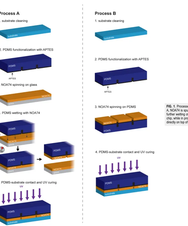
184) mixed in a ratio of 10:1 with its curing agent, was poured on top of the mold, degassed for 30 min in a desiccator, and baked at 80○C for 1.5 h in a convection oven. The metallized glass slides were coated with 15 nm of titanium, as an adhesion layer, and 150 nm of gold in a thermal evaporator (Kurt J. Lesker, Nano32).The PDMS-substrate bonding processes, shown inFig. 1, start with the substrate cleaning in deionized (DI) water and drying under a nitrogen stream. Then, after a plasma oxygen activation (25 W, 1 min), PDMS is functionalized with APTES (Sigma-Aldrich, #440140, 1% in DI water, 20 min at room temperature). The cor-rect functionalization was verified with a contact angle CAM 200 instrument (KSV Instruments, Helsinki, Finland) by acquiring 30 s videos of a DI water droplet dispensed by syringe and obtaining average ± standard deviation of the contact angle. Two bonding processes of the PDMS-substrate were tested. In process A, NOA74 (Norland Products) is spun on a glass slide (2000 rpm, 1 min) to create a thin and flat layer; the glue is then transferred to the PDMS surface by putting in contact the two surfaces (i.e., PDMS and glue-covered glass) for 5 s. In process B, NOA74 is directly spun on top of the PDMS at 6000 rpm. After the NOA74 layer is created on the PDMS surface, PDMS and substrate are put in contact and the glue is cured under a UV lamp (20 mW/cm2, 1.5 h). The thickness of the NOA74 layer was measured after spin coating on glass for
FIG. 1. Processes workflow. In process
A, NOA74 is spun on a glass slide for a further wetting of the PDMS microfluidic chip, while in process B, NOA74 is spun directly on top of the PDMS.
both processes A (2000 rpm) and B (6000 rpm) with a stylus pro-filometer (Bruker Dektak XT). Errors on the reported thicknesses are the standard deviation of at least 3 repeated measurements. The bonding process was tested on several substrates—PMMA (ARP 679.04, Allresist, GmbH, Strausberg, Germany, spun at 4000 rpm on a glass slide and dried overnight at room temperature), COC foils (thickness 140 μm, Microfluidic ChipShop GmbH, Jena,
Germany),15 PET foils (thickness: 250 μm, Coexpan, Montonate, Italy), and PS (cut from tissue culture Petri dishes, Falcon, Thermo Fisher Scientific)—and further confirmed also with a standard, com-mercially available, epoxy-based glue (Sigill, Pigal S.r.l., Bologna, Italy).
NOAs are UV-curable glues which contain epoxy groups.16,17 NOA74 is transparent and has low viscosity (∼90 cps) and excellent
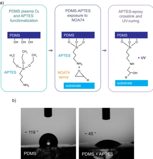
FIG. 2. PDMS functionalization with
APTES for further cross-linking. (a) Illus-tration of the role of the aminosilanes in creating a covalent bonding with the epoxy groups in NOA74. (b) Contact angles of a water droplet with bare PDMS and PDMS functionalized with APTES.
adhesion to metals, plastics, and glass.18Given the low viscosity of this glue, a thin adhesive layer can be easily realized by spin-coating. NOA74 thicknesses after spin-coating are 3.2 ± 0.3 μm for process A (spun at 2000 rpm) and 2.1 ± 0.1 μm for process B (spun at 6000 rpm). Without functionalizations, the PDMS surface is not wetted by this glue. Indeed, PDMS is often used as a mold for realizing NOA
structures, owing to their low reciprocal adhesion.19–21Thus, a direct bonding of the bare PDMS surface with NOA74 is not feasible. In order to overcome this issue, we functionalized the PDMS surface with APTES after plasma oxygen activation, providing amines for further cross-linking with the epoxy groups of NOA74. InFig. 2(a), an illustration of the main chemical processes involved is reported.
FIG. 3. Leakage tests setup. The
nitro-gen line goes through a 0.22μm
fil-ter and then into a pressure regulator which is set at 500 mbar when the MFCS is connected to the microfluidic device (blue path) or up to 2 bars when directly drives the input lines “in-1” and “in-2” (red path). A CCD was used to collect images and videos.
First, a plasma oxygen treatment of the PDMS is required in order to activate its surface. Then, the PDMS, exposing –OH groups, can be functionalized with APTES. We verified the PDMS functional-ization with APTES by measuring the water contact angle, which was 119○
± 2○ in the case of the untreated PDMS and 45○ ±5○ after functionalization [Fig. 2(b)], in agreement with the values reported in the literature.22The PDMS-APTES surface is then put in contact with NOA74 with two different processes (as described inFig. 1). In process A, the PDMS-APTES surface is wetted with NOA74 previously spun on glass, while in process B, the PDMS-APTES surface is coated with NOA74 by spin-coating. This step ends with the PDMS-APTES surface in contact with the NOA74-substrate [Fig. 2(a)central box]. In the last step, APTES bonds to the epoxy groups of the NOA74 and the glue is cured by UV expo-sure, providing the strong, irreversible bonding of the PDMS and the substrate.
With the aim of testing the two bonding processes for fluid leakage, we fabricated two PDMS microfluidic devices (one per pro-cess) with the same geometry bonded on gold-coated glass slides. These devices were further connected to the setup schematized inFig. 3. The PDMS microfluidic devices were composed by two microchambers (4 mm and 3.5 mm sides, 350 μm thick) separated by a 300 μm wall from an air-filled microchamber (top view in
Fig. 3). The two microchambers were connected to an inlet and out-let by a 350-μm-wide microchannel. This PDMS layer was bonded to a gold coated (150 nm thick) glass substrate, using process A or B (as described inFig. 1). For the leakage tests, we injected green and red dyes, one per microchamber, using a FLUIGENT
®
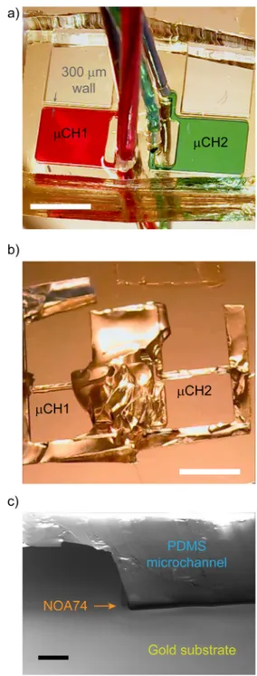
MFCS microfluidic pump under continuous monitoring with a CCD, as schematized inFig. 3. The applied pressures ranged from 0 to 70 mbar (Fig. 3blue path). The MFCS allows a maximum pressure of 500 mbar using the “PURGE” command. By repeating several injections of water, dyes, ethanol, and nitrogen from 0 to 70 mbar, and by using the 500 mbar purge (see videos in thesupplementary material), no leakage evidence was found. The tested pressure range is representative of a vast majority of microfluidics opera-tive conditions, but still below the benchmark PDMS-glass bonding strength achieved with the standard plasma oxygen procedure.12,23 Thus, in order to test higher pressures, we bypassed the MFCS and connected the pressure regulator directly to the liquid reser-voirs [Fig. 3 red path]. With this configuration, we could apply pressures up to 2 bars, the maximum value supported by our setup.Upon ethanol and nitrogen injection at a maximum pressure of 2 bars, neither leakage nor damage of the microchannels was obtained, as a proof of the strong bonding between the PDMS and the gold surface. Even after repeated cycles of pressurization, no device failures were observed. We did not observe any signif-icant expansion of the glue during the pressurization step. Even-tually, the microfluidic device could only be separated from the gold surface by ripping it apart with hands, leaving large residu-als on the surface, as is shown inFig. 4. During the leakage tests, in the case of process B, we occasionally observed chamber occlu-sion, owing to flooding of NOA74 that can occur during fabrication. In one case, this resulted in a complete clogging of the microchan-nel. NOA74 flooding is unavoidable in most cases for process B, being characterized by a direct NOA74 pouring onto the patterned PDMS surface. The NOA74 direct pouring and spin-coating steps of
FIG. 4. Leakage and unbonding tests. (a) Microfluidic chambers filled with red
(μCH1) and green (μCH2) dyes. (b) Residuals of the PDMS microfluidic channel after ripping it apart by hands. Scale bars in (a) and (b) are 4 mm. (c) The scanning electron micrograph of the PDMS residuals after ripping; the scale bar is 100μm.
process B, together with the channels geometry, could be the cause of the channels flooding. We therefore conclude that, while both pro-cesses can tightly seal PDMS on the substrate, process B can only be used for microchannels with a geometry that allow the spinning of a
the spinning-wetting steps that characterize process A are neces-sary in order to reach a finer control of the NOA74 spreading under the PDMS and avoid microchannel flooding/clogging. Nonetheless, process B requires fewer steps to be completed, and it is ideal for large structures.
After manual separation of PDMS from the gold layer, in the case of process A, we analyzed the remaining residuals of PDMS on the substrate by scanning electron microscopy. As expected, a NOA74 thin layer was observed only between the PDMS and the gold surface, with no evidence of NOA74 flooding inside the cham-ber [Fig. 4(c)]. Conversely, residuals of NOA74 could be found in the microchambers for process B. We also tested several microchan-nel widths (w = 10 μm, 50 μm, 100 μm) for evaluating the mini-mum w (wmin) that can be bonded with process A. We observed microchannel clogging forw equal to 10 μm and 50 μm, but not for w = 100 μm (Fig. S2). Therefore, we conclude that for process A 50 <wmin≤100 μm holds. The obtained wminalready covers a wide range of bondable microstructures for LOCs. Nonetheless, this does not exclude the possibility to further optimize the PDMS-wetting step, which is the most prone to determine the technique resolution and extend thewminto lower values.
The use of PDMS in microfluidics and LOCs still brings some difficulties owing to its hydrophobicity, nonspecific affinity to molecules, and gas permeability.24,25Indeed, during the last few years, many researchers have been putting effort into using other materials for realizing LOCs. To this purpose, our new process was successfully replicated with other nonmetallic substrates of interest for microfluidics, i.e., glass, PMMA, PS, PET, and COC (Table I), demonstrating its great versatility and potential for, but not limited to, microfluidic applications and LOC engineering. The choice of these materials was based on their growing interest not only in the LOC and microfluidics fields. In fact, glass and PMMA are already standard materials for substrates and microchannels, COC foils are frequently used in microscopy for their optical index similar to that of glass,26PS is the material of choice for cell cultures, and PET is a Food and Drug Administration approved material for food pack-aging. Remarkably, as a consequence of the optical transparency of the PDMS and the NOA74 glue, both processes A and B are com-patible with fine alignment instrumentation such as microscopes and mask aligners. These instruments are usually exploited with standard plasma-oxygen bonding for PDMS and glass.27Therefore, processes A and B can also be used whether a precise alignment between the microfluidic components and the substrates must be achieved. Furthermore, in order to confirm the broad applicability of TABLE I. List of tested materials as substrates. Gold and PMMA were used in the form of thin coatings.
List of tested substrates Gold Glass
Poly(methyl methacrylate) (PMMA) Polystyrene (PS)
Polyethylene terephthalate (PET) Cyclic olefin copolymer (COC)
able epoxy-based glues (see thesupplementary material). The results were in complete agreement with the NOA74 findings.
We have presented a novel technique for PDMS microchan-nels bonding on untreated plastic and metal surfaces. This process involves the use of, but it is not limited to, a UV-curable epoxy glue (NOA74) for the creation of a strong and stable bonding between PDMS and a great variety of substrates (glass, metals, and plas-tics). The PDMS microchannel is functionalized with APTES after a plasma oxygen activation, to allow the creation of a covalent bonding upon interaction with the epoxy groups of the glue, therefore provid-ing an irreversible sealprovid-ing of the device. Sealprovid-ing tests were performed in the case of two different processes (A and B) by injecting dyes and a gas in the PDMS microfluidic channels. Both processes resulted in a strong bonding with the surface, showing no leakage. Pressures could be applied up to 2 bars without any evidence of separation of the bound surfaces. Finally, the technique was successfully verified with other untreated substrates of interest in microfluidics, i.e., gold, glass, PMMA, PS, PET, and COC. As a remark, a plasma oxygen treatment of the substrate is not required, allowing a strong seal-ing even in cases where such a surface treatment is not feasible (e.g., functionalized surfaces, plasma-sensitive substrates). The versatility of this technique, along with its low complexity, makes it appealing for a great variety of applications in developing LOCs, allowing an unprecedented capability of bonding PDMS with nonfunctionalized noble metals (e.g., gold). This can be particularly useful for sealing structures as biosensors and actuators that can be damaged or can lose their functionalization if exposed to the conventional plasma oxygen treatment.
With the aim of demonstrating the broad applicability of the presented processes, we replicated the experiments with a common, commercially available, epoxy-based glue. The results are reported in thesupplementary material.
This work was supported by the “FAS14 GLIOMICS” project of “Regione Toscana”: proteomics/genomics/metabolomics for glioblastoma biomarkers discovery and their detection with an ultra-sensitive platform.
REFERENCES 1
E. K. Sackmann, A. L. Fulton, and D. J. Beebe,Nature507, 181 (2014). 2
D. Erickson, D. O’Dell, L. Jiang, V. Oncescu, A. Gumus, S. Lee, M. Mancuso, and S. Mehta,Lab Chip14, 3159 (2014).
3C. D. Chin, V. Linder, and S. K. Sia,Lab Chip
7, 41 (2007). 4R. Bashir,Adv. Drug Delivery Rev.
56, 1565 (2004). 5M.-I. Mohammed and M. P. Y. Desmulliez,Lab Chip
11, 569 (2011).
6Y. Temiz, R. D. Lovchik, G. V. Kaigala, and E. Delamarche,Microelectron. Eng. 132, 156 (2015) and references therein.
7
T. A. Duncombe, A. M. Tentori, and A. E. Herr,Nat. Rev. Mol. Cell Biol.16, 554 (2015).
8A. Sonato, M. Agostini, G. Ruffato, E. Gazzola, D. Liuni, G. Greco, M. Travagliati, M. Cecchini, and F. Romanato,Lab Chip16, 1224 (2016).
9
G. Greco, M. Agostini, S. Barone, and M. Cecchini,Sens. Actuators, B250, 525 (2017).
10M. Chu, T. T. Nguyen, E. K. Lee, J. L. Morival, and M. Khine,Lab Chip 17, 267 (2017).
11
M. Agostini, G. Greco, and M. Cecchini,Sens. Actuators, B254, 1 (2018). 12
13
C. S. Thompson and A. R. Abate,Lab Chip13, 632 (2013). 14
L. Tang and N. Y. Lee,Lab Chip10, 1274 (2010). 15
I. Tonazzini, A. Cecchini, Y. Elgersma, and M. Cecchini,Adv. Healthcare Mater. 3, 581 (2014).
16K. T. Kim, D. G. Kim, W. K. Hyun, K. B. Hong, K. Im, S. J. Baik, D. K. Kim, and H. Y. Choi,J. Opt. Soc. Korea12, 255 (2008).
17
S. M. Langelier, L. Y. Yeo, and J. R. Friend,Lab Chip12, 2970 (2012). 18
Seewww.norlandprod.com/adhchart.htmlfor detailed information about the NOA glues; accessed 02 October 2018.
19P. Wägli, A. Homsy, and N. F. De Rooij,Sens. Actuators, B
156, 994 (2011). 20H. Kim, Y. Yang, M. Kim, S. W. Nam, K. M. Lee, N. Y. Lee, Y. S. Kim, and S. Park,Adv. Funct. Mater.17, 3493 (2007).
21
E. P. Dupont, R. Luisier, and M. A. M. Gijs,Microelectron. Eng.87, 1253 (2010).
22
E. A. Smith and W. Chen,Langmuir24, 12405 (2008). 23
T. Squires and S. Quake,Rev. Mod. Phys.77, 977 (2005). 24
A. Gokaltun, M. L. Yarmush, A. Asatekin, and O. B. Usta,Technology5, 1 (2017).
25
D. A. Markov, E. M. Lillie, S. P. Garbett, and L. J. McCawley,Biomed. Microde-vices16, 91 (2014).
26C. Di Rienzo, E. Jacchetti, F. Cardarelli, R. Bizzarri, F. Beltram, and M. Cecchini, Sci. Rep.3, 1141 (2013).
27X. Li, Z. Yu, D. Geraldo, S. Weng, N. Alve, W. Dun, A. Kini, K. Patel, R. Shu, F. Zhang, G. Li, Q. Jin, and J. Fu,Rev. Sci. Instrum.86, 075008 (2015).