Chapter I – General Introduction
1
Chapter 1
General Introduction
1.1. Motivation
Carbon nanostructures, playing a central role in nanomaterials science and nanotechnology, are very attractive systems due to the wide diversity of their structural forms and peculiar properties.
When Lavoisier listed ‘‘Carbone’’ in his ‘‘Traite´ Elèmentaire de Chimie’’ as one of the newly identified chemical elements, for the first time just 220 years ago, he had already identified the versatility of carbon since he had shown that it was the elementary component of both diamond and graphite [1].
Since then, more allotropes of carbon have been reported and a large scientific community has been passionate about deciphering the properties of this element that can adopt many structures ranging from diamond and graphite (3D) to graphene (2D) [2], nanotubes (1D) [3] or fullerenes (0D) [4] as illustrated in Fig. 1.
The former three-dimensional allotropes have been known and widely used for centuries, whereas fullerenes and nanotubes have been only discovered and studied in the last two decades. With the exception of diamond, it is possible to think of fullerenes, nanotubes and graphite as different structures built from the same hexagonal array of sp2
carbon atoms, namely graphene. Indeed, fullerenes and nanotubes can be mentally visualized as a graphene sheet rolled into a spherical and cylindrical shape, respectively, and graphite can be described as a stack of alternately shifted graphene sheets.
Chapter I – General Introduction
2
Figure 1. Graphene is a 2D building material for carbon materials of all other dimensionalities.
Low-dimensional carbon allotropes: fullerene (0D),carbon nanotube (1D) and graphene (2D),[5].
The 2010 Nobel Prize in Physics honored Andre K. Geim and Konstantin S. Novoselov, who succeeded in producing, isolating, identifying, and characterizing graphene, [6].
Chapter I – General Introduction
3
The experimental isolation of single-layer graphene first and foremost yielded access to a large amount of interesting physics [8,9]. Initial studies included observations of graphene’s ambipolar field effect [2], the quantum Hall effect at room temperature [10-15], measurements of extremely high carrier mobility [16,17-19] and even the first ever detection of single molecule adsorption events [20,21]. These properties generated huge interest in the possible implementation of graphene in a myriad of devices, in part because two-dimensional crystals were thought to be thermodynamically unstable at finite temperatures [22,23].
The linear energy dispersion relation at low energies is a unique property among all known materials and it is an attractive one because it makes electron motion mimic the properties of photons. The practical consequence of this fact is the very high charge carrier mobility [24,25,26]. Infinitely large sheets of graphene are inherently two dimensional (2D) with zero bandgap.
The high mobility, the high current carrying capacity [27], the 2D or 1D atomic structure and the compatibility with planar technology makes graphene an exciting and promising addition to silicon-based CMOS. The novel band structure holds promise for as-yet unrealized devices that exploit the massless Dirac-fermion like linear energy dispersion of electrons in the material.
There are a number of motivations for using graphene-based devices in future nanotechnologies. Among them, the use of graphene can improve the electronic devices intrinsic performance and power efficiency or enable new functionalities, such as ultra-high-sensitivity detection for chemical and biological applications.
So far most of the research efforts on graphene-based electronics have been directed towards digital applications. However, conventional or even tunnel-based graphene FETs suffer from the lack of a well-defined energy gap, ultimately leading to poor on/off current ratios unless extremely narrow (1-2 nm) graphene nanoribbons are used as channel material. In analog applications, where the FET is used as an amplifier, the on/off problem is much more relaxed and the huge potential of graphene can be fully exploited.
Chapter I – General Introduction
4
In particular, the most promising analog applications for graphene electronics can be identified in high frequency low-noise amplifiers and/or power amplifiers, where the experimentally verified exceptional properties of respectively low-noise and high thermal conductivity, together with the high carrier drift velocity and mobility, are best exploited. The potential applications of graphene extend far beyond electronic devices. It is being touted as a material that will literally change our lives in the 21st century, like plastics did hundred years ago. Not only is graphene the thinnest (and lightest) possible material that is feasible, but it's also ~200 times stronger than steel and conducts both heat and electricity better than any material known to man – at room temperature. Potential applications for the material include replacing carbon fibers in composite materials, to eventually aiding the production of lighter aircrafts and satellites or stronger wind turbines; embedding the material in plastics to enable them to conduct electricity or just to make them stiffer, stronger, lighter or leak-tight; increasing the efficiency of electric batteries or supercapacitors by use of graphene powder; graphene based optoelectronic components promise closing the “terahertz gap” [28]; transparent conductive coatings for solar cells and (touch-enabled) displays; stronger medical implants; better sports equipment; artificial membranes for separating liquids; or nanogaps in graphene sheets may potentially provide a new technique for rapid DNA sequencing. Since graphene is so light, it holds a high potential in nanoelectromechanical (NEMs) systems and components and can usher in vast improvements in the speed of, for example, NEMs RF resonators to GHz frequencies. Graphene can be a part of future meta-materials built from stacks of other 2D materials such as BN or MoS2 [29,30].
These 2D materials have the inherent advantage of single layer nature with atomic smoothness, no dangling bonds or surface defects, high transparency and the possibility of easily controllable layer-by-layer growth. Such a device – including back insulation, channel, and gate oxide and interconnects – is not thicker than about 5 nm. Besides, there are no clear obstacles for the sub-10 nm lateral scaling either.
Chapter I – General Introduction
5
The future of graphene holds limitless possibilities into literally every corner of industry and manufacturing, and in the coming years it will likely become a commonplace substance, the way plastics are today.
While graphene has been known as a textbook structure to calculate band diagrams and predict unique electronic properties since the early 1940s, the experimental investigation of graphene properties, as a standalone object, has been almost inexistent until the very recent years because of the difficulty to identify and univocally characterize the single-atom thick sheet. Therefore, Fig.2 presents graphene identification data from (a) optical, (b) scanning probe and (c) electron microscopy as well as (d) ARPES, (e) Raman and (f) Rayleigh spectroscopy techniques.
Figure 2. Major techniques for graphene characterization. (a) optical microscopy, (b) atomic force
microscopy (AFM), (c) transmission electron microscopy (TEM),[31], (d) angle-resolved photoemission spectroscopy (ARPES), [32] (e) Raman scattering [33] and (f) Rayleigh scattering[34].
Chapter I – General Introduction
6
1.2. Outlines of the thesis
This work is dedicated to investigate the unique and excellent electrical and optical properties of graphene, through the fabrication and experimental study of several graphene based devices. Particular attention is paid to the details of all stages of the fabrication process which might have an effect on the properties of the final product. It also describes the characterization of graphene transistor structures, as well as experimental studies of charge transport.
I focused part of my research on optoelectronics and plasmonics of nanomaterials, in particular, I carried on a research that matched graphene and Plasmonics, the goal was to assess how the plasmonic response of metallic nanoparticles is modified by the presence of a graphene substrate, with results that could be very attractive as a starting point for the future optoelectronics applications.
This is how the thesis is planned: in the Chapter 2 I present a brief theoretical overview on the structural, electronic and optical properties of graphene.
In Chapter 3, I present the methods used for sample preparation, investigation of graphene flakes and the measurement setup. In particular, the identification of graphene is a very delicate step and involves the use of multiple techniques that complement each other. It is extremely difficult to find small graphene crystallites in the “haystack” of millions of thicker graphitic flakes. Thus, the identification is made by combining two or more of the following techniques: optical microscopy, Raman spectroscopy, SEM and the calculation of the contrast to give raise the best visibility.
The next, Chapter 4, is dedicated to the study of graphene based devices and their related features.
First, I fabricated 2D graphene FETs (GFETs) and explored several device designs to analyze transfer characteristic, mobility, and the influence of the contacts on the overall conductance.
The contacts between graphene and metal electrodes can significantly affect the electronic transport and limit or impede the full exploitation of the graphene intrinsic
Chapter I – General Introduction
7
properties. In this context I investigated the contact resistance on mono- and bi-layer graphene sheets by fabricating structures suitable for transfer length method measurements with Ni and Ti metals [36]. We also observed anomalies in GFET transfer characteristics, namely double dips, and here I present a work in which the origin of double dips in the transfer characteristics of GFET devices is explained [38]. In Chapter 5, I performed the characterization of Field Emission properties of several mono and bi layer graphene samples. I report the observation and characterization of field emission current from individual single- and few-layer graphene flakes laid on a flat SiO2/Si substrate. Measurements were performed in a scanning electron microscope chamber equipped with nanoprobes which allowed local measurement of the field emission current finding that the emission process is stable over a period of several hours and that it is well described by a Fowler–Nordheim model for currents over five orders of magnitude [37].
In the last Chapter 6, I present an exploration of the potential that electromagnetic surface waves known as surface plasmons may have in building both photonic elements and a new photonics technology based on nanostructured metals. I report results from an investigation into the plasmonic properties of metallic nanoparticles supported by substrates made of graphene, in order to extract information of its optical properties. In summary: the main accomplishments of this work are to:
a) The Set-up of a routine procedure to identify graphene samples and make their morphological characterization.
b) The fabrication of graphene based electronic devices, like graphene field effect transistors and non-volatile memories.
c) The Study of the influence of different metal contact on the overall conductance, and the investigation of anomalies in GFET.
d) The investigation of quantum tunneling phenomenon in graphene. e) The investigation of graphene as a substrate for plasmonics particles. These results will be presented in due course.
Chapter II – Properties of Graphene
8
Chapter 2
Properties of graphene
2.1. The graphene structure
Graphene is composed of sp2-bonded carbon atoms arranged in a two-dimensional
honeycomb lattice as shown in Fig. 3.
Figure 3. Atomic and electronic structures of graphene. (a) Graphene lattice consists of two
interpenetrating triangular sublattices, each with different colors. The atoms at the sites of one sub-lattice, (i.e. A) are at the centers of the triangles defined by the other lattice (i.e. B), with a carbon-to-carbon inter-atomic length of 1.42A°.
It has been studied theoretically for a long time as building block of graphitic materials in other dimensions [39]. The most famous allotrope of graphene is graphite, consisting of stacked graphene layers, held together only by weak Van der Waals forces.
The lattice can be seen as consisting of two interpenetrated triangular sub-lattices, for which the atoms of one sub-lattice are at the center of the triangles defined by the other with a carbon-to-carbon inter-atomic length, a C–C, of 1.42A. The unit cell comprises two carbon atoms and is invariant under a rotation of 120° around any atom.
Chapter II – Properties of Graphene
9
Each atom has one, s orbital, and two in-plane p orbitals contributing to the mechanical stability of the carbon sheet. The remaining p orbital, perpendicularly oriented to the molecular plane, hybridizes to form the π* (conduction) and π (valence) bands, which dominate the planar conduction phenomena [40].
2.2. Structural properties of Graphene
The structure can be seen as a triangular lattice with unit vectors a1 and a2, which enclose
an angle of 60°, spanning the unit cell as shown in Fig.4.
The unit cell has a diatomic basis comprising two equivalent carbon atoms A and B . The lattice vectors can be written as:
Figure 4. Hexagonal honeycomb lattice of graphene The primitive lattice vectors a1,2 are defining the unit cell. There are two carbon atoms per unit-cell, denoted by A and B. Also shown are the vectors to the first nearest neighbors of an A atom δ1,2,3
Chapter II – Properties of Graphene
10
Where a ≈ .4 Å is the nearest-neighbor C-C spacing, which is shorter than that in cubic diamond and the value of lattice constants is a1=a2 .46Ǻ .
When extending the graphene layer , we consider the other three next nearest neighbor vectors in real space, given by:
Starting from the unit vectors a1 and a2 the reciprocal lattice vectors b1 and b2 are
defined by the condition ai · bj = 2π δij. From that the first Brillouin zone of graphene is readily constructed (see Fig. 6).
Figure 5.
In reciprocal space, the first Brillouin zone also has hexagonal shape (Fig. 5, 6). Among the high-symmetry points, the points K and K’ at the corner of the Brillouin zone will be of special interest for the band structure.
Chapter II – Properties of Graphene
11
Figure 6. The equal energy contours are drawn, and the Brillouin zone (BZ) is indicated by dashed
lines. The Dirac points K and K’ are marked by arrows, and the reciprocal lattice vectors
are also
drawn. It is clear that the six points at the corners of the first Brillouin zone fall into two groups of three which are equivalent, so we need to consider only two equivalent corners that we denote as K and K’.
There are two types of graphene structure namely the zigzag and the armchair type. These structures differ according to the orientation and the direction of the edges. By looking at the figure and considering the edge along the y-axis, we see an armchair structure. Using the edge along the x-axis, it is possible to recognize the zigzag shape,
fig.7.
Chapter II – Properties of Graphene
12
2.3. Electronic band structure of the graphene lattice
After defining the lattice structure, the next step is to determine the band diagrams. One of the reasons justifying the interest in graphene lies in its energy band spectrum and in its electronic properties which are very special and different from standard semiconductors. Basically, according to their the electronic properties, materials are classified as metal, semi-metals, semiconductors or insulators. This classification is derived from the densities of states and band structures of the material.
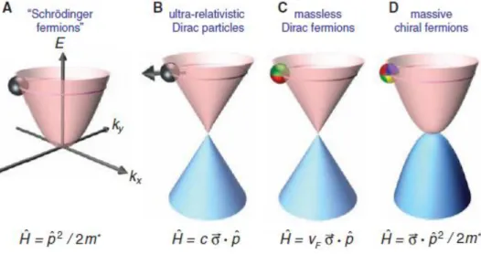
In condensed matter physics, the Schrödinger equation rules the world, usually being quite sufficient to describe electronic properties of materials.
Charge carriers in semiconductors have a non-zero effective mass, and their behavior can be well described by the Schrodinger equation.
Graphene is an exception: its charge carriers mimic relativistic particles and are easier and more natural to describe starting with the Dirac equation rather than the Schrödinger equation [41-49].
Figure 8. (A) Charge carriers in condensed matter physics are normally described by the Schrödinger
equation with an effective mass m* different from the free electron mass (p is the momentum operator). (B) Relativistic particles in the limit of zero rest mass follow the Dirac equation, where c is the speed of light and σ is the Pauli matrix. (C) Charge carriers in graphene are called massless Dirac fermions and are described by a 2D analog of the Dirac equation, with the Fermi velocity vF ≈ 1 × 10⁶
m/s playing the role of the speed of light .(D) Bilayer graphene provides us with yet another type of quasi-particles that have no analogies. They are massive Dirac fermions described by a rather bizarre Hamiltonian that combines features of both Dirac and Schrödinger equations. The pseudospin changes its color index four times as it moves among four carbon sublattices (2–4).
Chapter II – Properties of Graphene
13
Although there is nothing particularly relativistic about electrons moving around carbon atoms, their interaction with a periodic potential of graphene’s honeycomb lattice gives rise to new quasiparticles that at low energies E are accurately described by the (2+1)-dimensional Dirac equation with an effective speed of light vF≈106m/s. These
quasiparticles, called massless Dirac fermions, can be seen as electrons that lost their rest mass m0 or as neutrinos that acquired the electron charge e. The relativistic-like
description of electron waves on honeycomb lattices has been known theoretically for many years, never failing to attract attention, and the experimental discovery of graphene now provides a way to probe quantum electrodynamics (QED) phenomena by measuring graphene’s electronic properties.
In the high-energy limit, the linear energy–momentum relation is no longer valid and the bands are subjected to a distortion leading to anisotropy, also known as trigonal warping [6]. Upon stacking layers on top of each other, one first obtains bilayered graphene, which exhibits its own set of very specific properties. The center of the aromatic rings of the upper graphene sheet sits on top of an atom of the lower sheet, so that the symmetry is trigonal rather than hexagonal. With the inter-plane interaction, the charge carriers acquire a mass and the dispersion recovers a parabolic dispersion described by the Schrodinger formalism. Nevertheless, bilayer graphene remains gapless if one ignores trigonal warping.
The lateral confinement of the 2D lattice into nearly 1D ribbons causes band gap opening, which opens the possibilities to exploit the electronic properties of graphene in semiconductor device applications.
We use a “tight binding” (TB) or linear combination of atomic orbitals (LCAO) method for calculating the energy band structure, which stands as the basis of all electronic (and optical) properties of graphene. A common approximation is to neglect the on-site overlap (pz ground state energy) and the overlap between wave functions centered at
different atoms (i.e. the σ skeleton). The electrons populating the pz orbitals in the
Chapter II – Properties of Graphene
14
in which Φ(r) is the wave function for free electron moving in the electric field of isolated atom and Ckj are the Fourier coefficients. To construct periodic Bloch
functions, let , Ckj = N-1/2eik.Rj where N is the number of atoms in the system. Thus,
The band structure is calculated by evaluating the eigenvalues of the Hamiltonian matrix for the k values. The Hamiltonian of the system is in the form:
where is
The diagonal matrix elements represent the
p
z orbital ground state energy and can bechosen as the reference point of the energy i.e. to zero. The off-diagonals are given by:
where Φm
=
Φ(r-r
m) Usingρ
m=r
m-r
j to connect the matrix elementChapter II – Properties of Graphene
15
and
is the hopping parameter for the nearest neighbor. Its value for graphene is γ0 ~2.8 eV.
Plugging the coordinates of the nearest neighbors into the expression yields:
or
The eigenenergy of H(k) is specified by the secular equation:
We get the energy dispersion (or band structure) of 2D graphene to be:
This relation (plotted in Fig. 9) looks linear for low energies near the six corners (K or
Dirac-points) of the two-dimensional hexagonal Brillouin zone. Let’s call
k = K + dk and examine this linearity by expanding the expression for H12(k), eq.2.12,
Chapter II – Properties of Graphene 16
The Fermi velocity υF, is defined as
If we had expanded around K’ we would have obtained the complex conjugate of Eq.2.15. To determine the energy relation near the K point we can write the Hamiltonian in the form:
and the E-k relationship comes out in the form
Due to this linear dispersion relation at low energies, electrons and holes near these six points behave like relativistic particles described by the Dirac equation for spin 1/2 particles. That is why the electrons and holes are called Dirac fermions, and the six corners of the Brillouin zone are called the Dirac points.
The linear energy dispersion relation makes graphene quite different from most conventional three-dimensional semiconductors, which exhibit parabolic bands (energy is proportional to the square of the momentum) and a band gap. Intrinsic graphene can be thought of as a semi-metal, or a zero-gap semiconductor, as shown in Fig. 8.
Chapter II – Properties of Graphene
17
Figure 9. Energy bands of graphene. (left) Energy spectrum in units of γ0 = 2.8 eV (nearest neighbor
hopping energy) as a function of momentum ki. (right) Zoomed portion of the linear energy band near
the Dirac point. The maximum energy at k = 0 can be estimated from Eq.2.14
2.4. Carrier statistics and mobility in graphene (Inserire immagine)
Graphene’s quality clearly reveals itself in a pronounced ambipolar electric field effect (Fig.10) such that charge carriers can be tuned continuously between electrons and holes in concentrations n as high as 1.1013 cm-2 carrier concentration [50] and remarkably high
electron mobility at room temperature with reported values in excess of μ ~ 15 000 cm2/Vs.
Moreover, the observed mobility weakly depend on temperature T, which means that μ at 300K is still limited by impurity scattering and, therefore, can be improved significantly, perhaps, even up to ≈ 100,000 cm2/Vs.
Chapter II – Properties of Graphene
18
Although some semiconductors exhibit room-temperature μ as high as ≈ 77,000 cm2/Vs
(namely, InSb), those values are quoted for undoped bulk semiconductors. In graphene, μ remains high even at high n (>1012cm-2) in both electrically and chemically- doped
devices [51] , which translates into ballistic transport on submicron scale (up to ≈0.3 μm at 300K).
Figure 10. Ballistic electron transport in graphene. Ambipolar electric field effect in single-layer
graphene. The insets show its conical low-energy spectrum E(k), indicating changes in the position of the Fermi energy EF with changing gate voltage Vg. Positive (negative) Vg induce electrons (holes) in
concentrations n =αVg where the coefficient α ≈7.2·1010cm-2/V for field-effect devices with a 300 nm
SiO2 layer used as a dielectric [52-54]. The rapid decrease in resistivity ρ with adding charge carriers indicates their high mobility (in this case, μ ≈ 15,000cm2/Vs and does not noticeably change with
temperature up to 300K).
Scattering by acoustic phonons in graphene limits the low field room temperature μ to 200 000 cm2/Vs at a carrier density of n ~ 2.1011 cm−2, which was experimentally
achieved in suspended graphene [25]. However, for graphene in contact with oxides or dielectrics, scattering of electrons by optical phonons of the substrate dominates at room temperature.
Chapter II – Properties of Graphene
19
The intrinsic optical phonon energy in graphene is ωop ≈ 160 meV, thus emission is not possible in the case of low energy transport. It has been shown that the surface optical (SO) phonon energy of common dielectrics is lower, in the 20 – 80 meV range [55].
Impurity scattering can be an important factor too, depending on the impurity concentration of the substrates. High-κ dielectrics have lower energy SO modes thus the mobility has a lower limit. On the other hand the higher dielectric constant screens the impurity charges more effectively. The two competing effects renders the maximum achievable mobility to ~10 000 cm2/Vs at room temperature and is more or less
independent of the choice of the dielectric at nimp~5.1011 cm-2 impurity concentration
and at n ~ 1012 cm-2 charge density [55].
The relation between the scattering rate 1/τ and mobility in semiconductors is
μ = τq/m*, where q is the electron charge and m* is the effective mass.
For graphene it is [56]:
where νF is the Fermi velocity and n is the carrier concentration.
Equation 2.20, turns the attention towards an interesting fact, namely that the mobility is highly dependent on the carrier concentration in graphene, which is examined in detail in the following.
Using the energy dispersion relation of graphene, which is conical at low energies (Eq. 2.19) to determine the 2D density of states (ρ(E) kdk/π, DOS), it can be written:
Chapter II – Properties of Graphene
20
where
g
v=2
is the valley degeneracy andg
s=2
is the spin degeneracy. Only some ofthese states are populated by carriers and it is defined by the Fermi-Dirac distribution at a given Fermi level EF:
To find the electron density, the product of the Fermi-Dirac distribution and the DOS has to be integrated over the whole energy range:
The integral can be evaluated [31] if we introduce u = E/kT and η = EF/kT:
Where
is the Fermi-Dirac integral with j Γ(…) is the gamma function and the sign on η is
+ for electrons and – for holes. In the special case when the Fermi level is at 0eV Eq. (2.24) simplifies to:
Where ni is called the intrinsic carrier concentration. Unlike in case of materials with
bandgaps, the intrinsic carrier concentration in graphene does not depend exponentially on temperature, but quadratically.
Chapter II – Properties of Graphene
21
This is a very interesting and unique phenomena but it has not yet been observed because it requires samples with very low residual impurity concentration. A way to get rid of the effect of impurities is to suspend graphene.
It is well known that mobility is a function of carrier concentration in graphene and very high mobility values can be obtained only at very low carrier concentrations.
Starting from the equation for the drift current of a graphene FET:
where n is the 2D carrier concentration, and E is the electric field along the channel. The conductivity is σ=J/E, and one can extract the mobility specifically for a 2D graphene field effect transistor geometry:
where e is the electron charge, n is the 2D carrier concentration, LG is the gate length, W is the channel width, VDS is the source-drain bias, VGS is the gate bias and V0 is the
threshold-or Dirac-point voltage. This definition of the mobility is inversely proportional to carrier concentration therefore it gives extremely high mobility values for low carrier concentrations. This can be called conductance based mobility (μCON). We can also define a field-effect mobility (μFE) as the change in the sheet conductivity of graphene due to carrier density modulation Δn as:
The expression can be modified to the form:
Chapter II – Properties of Graphene
22
Where gm=dID/dVGS is the transconductance. As opposed to μCON the field-effect
mobility μFE goes to zero at the lowest carrier concentrations at the Dirac point, since
the drain current reaches a minimum when the gate bias equals the Dirac point, and by definition gm=dID/dVGS=0.
2.5. Some interesting properties
2.5.1.1. Stability in two dimensions
The fact that two-dimensional atomic crystals do exist, and moreover, are stable under ambient conditions [148] is amazing.
More than 70 years ago, Landau and Peierls argued that strictly two-dimensional (2D) crystals were thermodynamically unstable and could not exist.
A standard description [149] of atomic motion in solids assumes that amplitudes of atomic vibration u near their equilibrium position are much smaller than interatomic distances d, otherwise the crystal would melt according to an empirical Lindemann criterion (at the melting point, u ≈ 0.1d).
For instance, the melting temperature of thin films rapidly decreases with decreasing thickness, and they become unstable (segregate into islands or decompose) at a thickness of, typically, dozens of atomic layers. For this reason, atomic monolayers have so far been known only as an integral part of larger 3D structures.
The argument was later extended by Mermin [147] and is strongly supported by a whole omnibus of experimental observations.
Chapter II – Properties of Graphene
23
As a result of this small amplitude, the thermodynamics of solids can be successfully described using a picture of an ideal gas of phonons, i.e. quanta of atomic displacement waves (harmonic approximation).
In three-dimensional systems, this view is self-consistent in a sense that fluctuations of atomic positions calculated in the harmonic approximation do indeed turn out to be small, at least at low enough temperatures.
In contrast, in a two-dimensional crystal, the number of long-wavelength phonons diverges at low temperatures and, thus, the amplitudes of interatomic displacements calculated in the harmonic approximation diverge [150-151].
According to similar arguments, a flexible membrane embedded in three-dimensional space should be crumpled because of dangerous long-wavelength bending fluctuations [152]. However, in the past 20 years, theoreticians have demonstrated that these dangerous fluctuations can be suppressed by inharmonic (nonlinear) coupling between bending and stretching modes [152-154]. As a result, single-crystalline membranes can exist but should be ‘rippled’. This gives rise to ‘roughness fluctuations’ with a typical height that scales with sample size L as Lζ, with ζ ≈ 0.6. Indeed, ripples, fig. 11, are observed in graphene, and play an important role in its electronic properties [154].
Figure 11: Illustration of a single-layer graphene sheet with out-of-plane corrugations. The
thermodynamic stability of the 2D crystal is believed to be accounted for mainly by such ripples [7]. (Image source: J. Meyer [7])
Chapter II – Properties of Graphene
24
2.5.1.2. Anomalous Integer Quantum Hall Effect
Classically, an electrical conductor carrying a current I in a perpendicular magnetic field
B⊥ will show a potential difference Uxy= UH across the opposite sides of the conductor.
The hall resistance RH = UH/I = −B⊥/(n·e·t) is the ratio of the potential drop divided
by the current, where n is the charge carrier density, e is the electron charge, and t is the thickness of the conductor. The Hall Effect is a consequence of the Lorentz force acting on the charge carriers: the transverse magnetic field deflects the carriers, causing them to accumulate at one side of the conductor.
In two dimensional electron gases (2DEGs) at low temperatures and high magnetic fields, it was found [57] that the Hall conductivity σH = ρH−1 takes on discrete values of
Where h is the Planck constant, e is the electron charge and
ν
is due to the spin and thevalley degeneracy of the 2DEG. This is due to the fact that in a perpendicular magnetic field, the electrons in the 2DEG are forced to move in quantized cyclotron orbits with discrete energy levels. These energies, known as Landau levels (LLs), are given by:
Where ωc = eB/m is the cyclotron frequency. The Hall conductivity σH remains constant when the Fermi energy EF is between two LLs and increases by a discrete value, when EF passes the next higher LL.
Chapter II – Properties of Graphene
25
Figure 12. (Left) Landau levels for Schrödinger electrons with two parabolic bands touching each
other at zero energy. (Right) Landau levels for Dirac electrons.
The QHE in single layer graphene (SLG) differs from that in conventional 2DEGs in the sense that the Hall conductivity plateaus are shifted [4] and form at
This so-called half-integer QHE of SLG was first measured by Novoselov et al. [54] (see
fig.13) and Zhang et al. [58]. The reason for this shift of 2e2/h is that in graphene, the LL energies are given by:
An important peculiarity of the Landau levels for massless Dirac fermions is the existence of zero-energy states (with ν = 0 and a minus sign in the equation).
Chapter II – Properties of Graphene
26
Figure 13: QHE measurements at 4 K/14 T of a single layer graphene device by Novoselov et al.
[54].The Hall conductivity σxy = ρ−1H as a function of the carrier concentration n forms plateaus at
half-integer values of 4e2/h (red curve), while the longitudinal resistivity ρ
xx vanishes at these values of n
(blue curve).
This situation differs markedly from conventional semiconductors with parabolic bands where the first Landau level is shifted by ½hωc. As shown by the Manchester and Columbia groups [54,58] the existence of the zero-energy Landau level leads to an anomalous QHE with half-integer quantization of the Hall conductivity (Fig.13),
instead of an integer one (for a review of the QHE, see, for example [59]). Usually, all
Landau levels have the same degeneracy (number of electron states with a given energy), which is proportional to the magnetic flux through the system. As a result, the plateaus in the Hall conductivity corresponding to the filling of first ν levels are integers (in units of the conductance quantum e2/h). For the case of massless Dirac electrons, the
zero-energy Landau level has half the degeneracy of any other level.
This anomalous QHE is the most direct evidence for Dirac fermions in graphene [15, 16].
Chapter II – Properties of Graphene
27
2.5.1.3. Klein paradox
Quantum tunneling
Quantum tunneling is a consequence of very general laws of quantum mechanics, such as the Heisenberg uncertainty relations. A classical particle cannot propagate through a region where its potential energy is higher than its total energy . However, because of the uncertainty principle, it is impossible to know the exact values of a quantum particle’s coordinates and velocity, and thus its kinetic and potential energy, at the same time instant. Therefore, penetration through the ‘classically forbidden’ region turns out to be possible. This phenomenon is widely used in modern electronics, beginning with the pioneering work of Esaki [60].
When a potential barrier is smaller than the gap separating electron and hole bands in semiconductors, the penetration probability decays exponentially with the barrier height and width. Otherwise, resonant tunneling is possible when the energy of the propagating electron coincides with one of the hole energy levels inside the barrier.
Surprisingly, in the case of graphene, the transmission probability for normally incident electrons is always equal to unity, irrespective of the height and width of the barrier [61-63].
In QED, this behavior is related to the Klein paradox [61,64-66]. This phenomenon usually refers to a counterintuitive relativistic process in which an incoming electron starts penetrating through a potential barrier, if the barrier height exceeds twice the electron’s rest energy mc2. In this case, the transmission probability T depends only
weakly on barrier height, approaching perfect transparency for very high barriers, in stark contrast to conventional, and non relativistic tunneling. This relativistic effect can be attributed to the fact that a sufficiently strong potential, being repulsive for electrons, is attractive to positrons, and results in positron states inside the barrier. These align in energy with the electron continuum outside the barrier. Matching between electron and positron wave functions across the barrier leads to the high probability tunneling described by the Klein paradox.
Chapter II – Properties of Graphene
28
In other words, it reflects an essential difference between non relativistic and relativistic quantum mechanics. In the former case, we can measure accurately either the position of the electron or its velocity, but not both simultaneously. In relativistic quantum mechanics, we cannot measure even electron position with arbitrary accuracy since, if we try to do this, we create electron-positron pairs from the vacuum and we cannot distinguish our original electron from these newly created electrons.
We first note that the wave function for Dirac fermions in graphene can be given by:
where Φ(k) = tan-1 ky/kx. We now consider scattering by a finite potential well of
magnitude V0 and width D, as shown in fig.14. There are thus three regions as marked in the figure. In region I, we have:
Which has a right and left moving component, where s =±1, and in polar coordinates, and considering fermions with Fermi momentum kF , we have ky = kF sin Φ(k) and kx = kF cos Φ(k). In region II:
Chapter II – Properties of Graphene
29
Figure 14: The proposed setup to demonstrate the Klein paradox. An incoming Dirac Fermion hits a
finite potential well of magnitude V0 and width D. The transmission is calculated as usual in elementary
quantum mechanics by demanding the continuity of the wave functions. Figure from reference [67]
Where θ = tan-1 k
y/qx and
and for the region III we have only a
right moving component:
Chapter II – Properties of Graphene
30
Where s = sign(E) and s’ = sign(E-V0). According to the standard prescription, the coefficients of the wave functions must be determined such that continuity is preserved at the boundaries x = 0, D, but the derivative need not be matched in this case, unlike with the Schrodinger equation. The transmission as a function of incident angle is T(Φ) = tt*, and is given by:
What is unusual about this result is that for Dqx = nπ, the barrier becomes completely
transparent (T(Φ) = 1), which includes normal incidence (Φ 0).
This is the Klein paradox, and is unique for relativistic electrons. Some nice results are reported in fig.16 , where, depending on the value of V0, there are several points with
complete transmission.
Figure 15. The transmission results from equation 7 for different values of V0, where D = 110nm
(top), and D = 50nm (bottom). Aside from normal incidence there are potentially other points of absolute transmission as well. This absolute transmission is a manifestation of the Klein paradox. Figure from reference [67]
Chapter II – Properties of Graphene
31
2.5.1.4. DOS for Graphene and Semiconductors
Fig. 16 shows a comparison between the electronic structure of graphene and a
two-dimensional electron gas (2DEG) in a standard semiconductor. The band structure of graphene has a linear dispersion, and valence and conductance band touch at the K and K’ points: E(q) ≈ ±~ђυF |q| (Fig. 16(a)). Considering the fourfold degeneracy due to
spin and valley degeneracy, this dispersion relation leads to a two-dimensional density of states D2D(E) = 2|E|/πђ2υ2
F. The density of states is linear in energy and vanishes at
the Dirac point for ideal graphene. (Fig. 16(b)).
The dispersion relation of a typical direct band gap semiconductor is depicted in Fig.
16(c). It is parabolic with a gap between valence and conductance band.
The conductance band dispersion can be described as E = EC + ђ2k2/2m* , for the
valence band it is similar. The two-dimensional density of states is zero for the region of
the band gap, and constant in the valence and conductance band region:
D2D(E) = m*/ πђ2.
Figure 16: Comparison between graphene and standard 2D semiconductor electron gases. (a)
Schematic drawing of the band structure of graphene around the K-point. (b) Density of states of graphene. (c) Schematic drawing of the band structure of a standard semiconductor with direct band gap. (d) 2D density of states for a standard semiconductor.
Chapter II – Properties of Graphene
32
The unusual properties mentioned here are just a few examples of the many interesting properties of graphene based materials. The literature on graphene, despite its relatively young age, is enormous, and it is almost impossible for one to keep abreast of the rapid progress that this field is currently undergoing. This makes graphene an exciting field to be involved in.
2.6. Optical properties
Graphene can be profitably used in photovoltaics, thanks to the remarkably high optical transmission over a wide spectral range, coupled to the mentioned high electron mobility, extremely useful for charge collection in solar cells [68, 69].
In optoelectronics, graphene based devices have been designed and studied for high-speed radiation detection [70], light emission from organic LED [71], as transparent conductive sheets substitutive of ITO, for example for touchscreens, liquid crystal displays or photovoltaic cells [72-74], or ultracapacitors for energy storage [75], and solid state mode-lockers in fiber lasers [76].
In view of the optimization of the graphene performances, it is evident that optical properties, such as reflectance, transmittance and absorption, deserve particular attention.
In general the optical properties of graphene are governed by its dynamical conductivity
σ (ω). For frequencies greater than the typical inverse scattering time ω>> t−1 the optical
conductivity σ (ω) within a single-particle tight-binding theory can be written as [77, 78] :
where f0 = (exp[(e − μ)/kBT] + 1)−1 is the Fermi function, μ is the chemical potential,
kB is Boltzmann’s constant, and T is the temperature. The first integration in Eq.2.30 gives the contribution from intraband processes, which after integration read as:
Chapter II – Properties of Graphene
33
which for temperatures kBT << μ reduces to
The second term in equation 2.30 describes the contribution to the conductivity from interband processes.
After integration of the second term we arrive at
Where θ(ω − 2μ) is the step function. We can see that for transition frequencies
ω >>μ , the logarithmic singularity is cut off with the temperature and the expression
for σ inter reduces to:
This result has important implications for the optical properties of graphene. Since σ inter
is constant, optical properties such as the transmission T and absorption A should also be constant according to:
Chapter II – Properties of Graphene
34
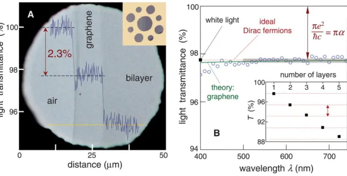
The relationship A = 1 − T holds because the reflectance R is negligible (R = 1/4π2a2T
< 0.1%). Experimental verification of this theoretical prediction has been given by Nair et al. [79] Fig. 17 shows the results obtained by Nair et al..
For light transmission throughout the visible, graphene indeed only absorbs 2.3% of impinging light. Further, absorption as a function of graphene layers is additive which points towards a negligible interlayer coupling with respect to the optical properties of graphene.
Figure 17: Universal transmission of graphene. (a) Experimental setup for measuring the optical
transmission of graphene; micromechanical exfoliation of graphene on a copper grids with apertures of varying size. (b) Constant transmission through a freely suspended graphene layer over visible wavelength range. The inset shows transmission values as a function of the number of graphene layers. Images are taken from [79]
Chapter III – Graphene Production and graphene characterization techniques
35
Chapter 3
Graphene production and graphene
characterization techniques
3.1. Introduction
Despite the intense interest and the continually experimental progress, widespread implementation of graphene devices has yet to occur. This is primarily due to the difficulty of reliably producing high quality samples, especially in any scalable fashion [80]. The challenge is really 2-fold because performance depends on both the number of layers present and the overall quality of the crystal lattice [81- 84]. So far, the original top-down approach of mechanical exfoliation has produced the highest quality samples, and a number of alternative approaches to obtaining single layers have been explored. One of the key elements in graphene discovery, and still nowadays in handling it in most studies, resides in the use of an appropriate substrate that maximizes the optical contrast of the carbon atom monolayer in the wavelength range of maximal sensitivity for the experimentalist.
3.2. Graphene production
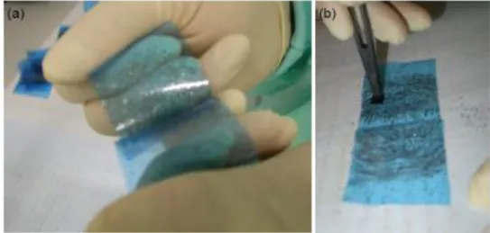
In all my experiments single layer graphene was produced by a micromechanical cleavage exfoliation technique by sticky “scotch”-tape of graphite to peel-off a few layers of graphene.
Graphite is a polycrystalline material originating from one of the following sources:
1. Highly Ordered Pyrolytic Graphite (HOPG); 2. Kish graphite;
Chapter III – Graphene Production and graphene characterization techniques
36
HOPG is a synthetic product widely used in different scientific experiments as a substrate. The controlled growth of HOPG, based on thermal decomposition of hydrocarbon, allows it to be chemically clean and AB stacked, however it may still have lattice defects, and it was principally used in this thesis for graphene production.
The second type, Kish graphite is a byproduct of the metal industry and is produced during the cooling of molten steel. Therefore, it is expected to have metallic impurities, yet can also be chemically purified. Natural graphite is mined around the world in the form of a lump, amorphous and crystalline flake graphite and its properties strongly depend on the geography. However, even good quality monocrystals of natural graphite may contain up to 5 % of rhombohedral phase which is known to have smaller average interlayer distance [102]. The choice of this particular type is based on the big lateral size of monocrystalline areas it is made of and therefore the big size of graphene flakes extracted (up to 50 µm).
Figure 18: Hexagonal graphite lattice arranged in Bernal A-B stacking. SEM image of natural graphite,
scale bar 100 µm.
Part of the fabrication process took place in a cleanroom. Since the air is a complicated mixture of common gases (nitrogen, oxygen, argon, carbon dioxide etc.) and a large number of traces of other species, it is impossible to count all contaminants arriving at a flake surface during and after its fabrication. In the ideal case graphene should not be exposed to the air, but this is difficult to achieve and at present moment no methods
Chapter III – Graphene Production and graphene characterization techniques
37
have been reported whereby a graphene flake is always kept (when fabricated and measured) in a clean, controlled atmosphere.
An adsorption process is usually classified as chemisorption (e.g., a covalent bond formation) or physisorption (weak van der Waals forces), depending on the type of the force responsible for the attractive interaction. Graphene will easily physisorb different atoms and molecules and their presence can influence the charge transport. If the surface is heated, the energy transferred to the adsorbed species will cause it to desorb. Thus, in the presence of such species in the environment, there will be a dynamical balance between incoming and leaving adsorbates. The rate of leaving follows an activation rule, ∝ x exp (−u/RT), where x is the fraction of the surface covered by adsorbate, u is the binding energy and T is the temperature of the surface. The rate of arriving is ∝ (1 − x) p, where p is the partial pressure of the vapor. Therefore a contaminated surface can be cleaned by increasing its temperature (annealing) in a clean environment.
3.3. Experimental method for graphene fabrication
In order to locate and contact graphene flakes, an orientation grid is needed on the substrate, fig.19. Usually this is done by writing a matrix of cross-like markers or number referenced markers, fig.20, using electron beam lithography (EBL) and then evaporating Ti/Au or Cr/Au (2 nm/40 nm) and lift-off.
Chapter III – Graphene Production and graphene characterization techniques
38
Figure 20. A grid referenced-markers The distance is 75um along x and 40um along y .
So the wafers needed a cleaning treatment prior to graphene deposition, in fact, the surface can potentially get contaminated during the shipping and storage.
Here, I report two cleaning methods that I used:
1st Method
Acetone, room temperature (ultrasonic aggravation, 5-10 minutes), wet transfer to IPA, room temperature (ultrasonic aggravation, 5-10 minutes),
dry in N2 flow.
2nd Method
Acetone, boil 56∘C (ultrasonic aggravation, 5-10 minutes), wet transfer to IPA, room temperature (ultrasonic aggravation, 5-10 minutes),
dry in N2 flow.
The first method is a standard method of cleaning. The second is a more aggressive version of the first, utilizing normal behavior of organic solvents to increase its reactive ability at higher temperatures.
At this point, the exfoliation method took place: it consist to use a common adhesive tape and to repeat the stick and peel process a dozen times which statistically brings a 1 µm thick graphite flake to a monolayer thin sample.
Chapter III – Graphene Production and graphene characterization techniques
39
Because the inter-layer Van der Waals interaction energy is of about 2 eV/nm2, and the
order of magnitude of the force required to exfoliate graphite is about 300 nN/µm2 [85],
this extremely weak force can be easily achieved with an adhesive tape.
Historically, the first method that succeeded in the isolation of a single graphene sheet has been the micromechanical exfoliation of highly oriented pyrolytic graphite (HOPG) in the very simple fashion method developed by Novoselov et al. in 2004 [2, 53,86].
Figure 21. Single layer graphene was first observed by Geim and others at Manchester University. Here
a few layer flake is shown, with optical contrast enhanced by an interference effect at a carefully chosen thickness of oxide.
In principle, any adhesive tape could be used for the cleavage of graphite into graphene, but we use single-side adhesive ‘Nitto’ tape (SWT-20), which is used in the semiconductor industry for wafer protection. The tape consists of a specially formulated acrylic adhesive ∼ 10 µm thick on a PVC film carrier.
A small piece of graphite (usually a few mm lateral size and less than 100 µm thick) is placed between two pieces of the tape and then two tapes are torn asunder, splitting the graphite piece into halves (Fig.22).
Chapter III – Graphene Production and graphene characterization techniques
40
Figure 22. Nitto adhesive tape (blue) with graphite flakes (black)
This procedure is repeated a few times until the graphite covers a significant area on the tape surface and in order to cleave the graphite into thinner flakes (Fig. 23), so, each part has to be thinner than the original one.
Between five and ten folding events is a good number: if the tape is folded less often, the graphite is not cleaved enough, and the resulting graphene flakes are too thick. If folded too many times, the graphene flakes become smaller, with more glue residues. In a next step, the graphene flakes are transferred onto a wafer prepared with the alignment markers.
Figure 23: Deposition of graphene (a) Folding of the sticky tape, covered with graphite flakes (b) Transfer of the flakes from the tape to the Si/SiO2 substrate.
Chapter III – Graphene Production and graphene characterization techniques
41
A chip is placed on top of the tape in a region where it is uniformly covered by graphite exfoliated, and then pressed against a freshly cleaned wafer with a pressure of 100 N/cm2 with tweezers or with a finger, and removed straight away. This creates many
flakes on the surface of the wafer with a variety of thicknesses from a monolayer up to a few microns held by the Van der Waals force. Once the tape is attached to the surface, the best result usually comes with the force applied perpendicular to the surface. Increasing the vertical pressure leads to an increase in the total flake density but can damage the surface oxide layer and leaves unwanted dust.
Typically, graphite flakes occupy a few percent (0-5 %) of the total wafer area. The presence of organic contamination (e.g. skin secretion, exhaled air, vacuum grease) on the surface often increases the flake adhesion and therefore the covering ratio.
After a number of graphene depositions done according to the procedure explained above, we have found that two depositions done in exactly the same way do not result in the same average flake density. The reason for this can be that the adhesion force depends on the environmental conditions.
So, another technique could be used: once the tape is attached to the surface of the chip, without pressing each other, it is possible to keep them in a vacuum chamber for 24 hours, and finally remove the tape gently.
The action of the pressure in the chamber that decreases the value regularly up to 10-6Torr, plays the rule to press uniformly the tape on the all surface. The effect is to
increase the total flake density and to improve the flake adhesion on the surface.
After removing the sample from the tape, glue residues can to be left on the sample, so limiting the carrier mobility [89,90]. A post-deposition cleaning and heat treatment, as well, is thus required to remove the residue.
Therefore, as already said, the chips are cleaned in acetone and isopropanol, and a short ultrasonic pulse is applied to make sure the flakes chosen for processing in the next step stick well to the surface, and if possible followed by 2 min of oxygen plasma ashing. Others graphene preparation is attempted by different approaches, one of this that is a more “scalable” method to produce graphene is to grow it on a suitable planar surface using chemical vapor deposition (CVD), molecular beam epitaxy (MBE), or by the
Chapter III – Graphene Production and graphene characterization techniques
42
reduction of SiC [93-95]. These methods can now produce both multilayer and single-layer graphene on large-area substrates. The clear advantage is that one can cover an entire wafer with graphene by such growth methods.
Neverthless, despite tremendous progress with alternatives, mechanical exfoliation with cellophane tape still produces the highest quality graphene flakes available and it remains the best method in terms of electrical and structural quality of the obtained graphene, primarily because it benefits from the high-quality of the starting single crystalline graphite source. The size of the deposit is also appreciable, and can be purchased on supporting substrate in the fraction of square millimeter. However it will be challenging to bring this approach to large scale production level, which is why other strategies have attracted a renewed interest.
3.4. Techniques for the detection and characterization of
graphene flakes
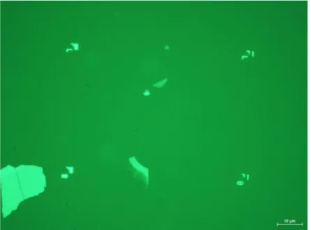
After the deposition, the chip is covered by many graphene flakes of different thicknesses. An optical microscope (Nikon Eclipse LV-150) is used to detect thin flakes
Fig.24.
Figure 24: Optical Microscope and an image of the graphene flakes of
Chapter III – Graphene Production and graphene characterization techniques
43
3.4.1.1. Optical Microscope
The visibility of graphene has been studied theoretically [103] and experimentally [104]. Optical microscopy is a technique that allows to quickly discern the thickness before moving on to more precise and less direct methods such as Raman spectroscopy, used to selectively investigate small portions of the sample.
The advantages of the optical microscope imaging are: i) graphene can be viewed optically with minimal magnification (4x, 10x, 20x, 40x, 100x); ii) Approximate thickness is determined by color (black, white, blue, purple, pink).
Disadvantages of this technique lie on: the uncertainty of the identification and the invisibility of graphene when using an unsuitable substrate and/or inadequate source wavelength [103].
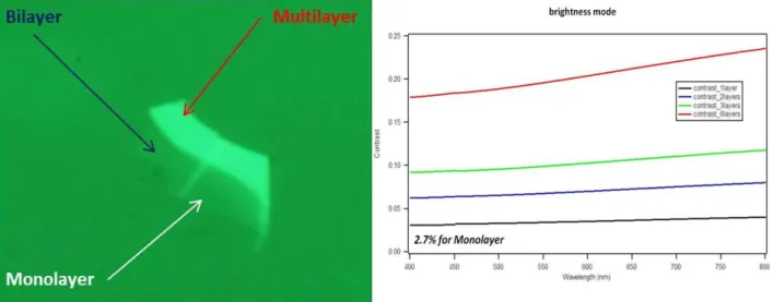
3.4.1.2. Study of contrast for rapid identification of Graphene
Graphene flakes with various thicknesses both single layer graphene (SLG) and few layer graphene (FLG), once the flakes are deposited on a dielectric substrate, can be rapidly identified by white light contrast analysis via an optical microscopy survey [2].
Contrast in optical image strongly depends on many parameters [110, 111]: the incident angle of the light source, the luminance of the source, the thickness of the dielectric film, the dielectric material, the substrate of the thin dielectric film, and, obviously, on the graphene flake thickness.
This rapid identification mechanism, is essentially based on the contrast raising from the interference of the reflected light beams at the air-to- graphene, graphene-to-dielectric and (in case of thin dielectric films) dielectric-to-substrate interfaces [103].
The thickness of the oxide layer has to be carefully chosen. It was shown that the flake’s contrast oscillates as a function of the oxide thickness, due to the interference of the reflected light., and only for very specific thicknesses, the contrast of a single graphene layer is strong enough to be detected in white light due to the flake’s opacity and the increased optical path [13].
Chapter III – Graphene Production and graphene characterization techniques
44
Thin films of SiO2/Si(100) (300 nm) are the typical substrates used for such a rapid identification [109], for which the apparent contrast of graphene monolayer is at about 12% at 550 nm, where the sensitivity of the human eye is optimal. This phenomenon is easily understood by considering a Fabry–Perot multilayer cavity in which the optical path added by graphene to the interference of the SiO2/Si system is maximized for specific oxide thicknesses [86, 87, 88].
Graphene is not completely transparent to the light source radiation, but it is visible thanks to the changes of optical paths of the light through the oxide thickness.
We can explain this phenomenon using Fresnel theory, a model for reflection and transmission of graphene based on normalized conductance that does not require the use of graphene's refractive index, but rather the use of the optical conductance.
Figure 25. Optical paths of the light on Graphene/SiO2/Si structure
The universal optical conductance of a graphene monolayer in the limit of massless Dirac fermion bandstructure is Z0=e2/ 4 . By normalizing the optical conductance with
free space impedance Z0 we have:
where α is the fine structure constant. The universal conductance, when normalized by the impedance of free space, is a fundamental physical constant independent of unit system.
Chapter III – Graphene Production and graphene characterization techniques
45
If m is the number of graphene layer normalized conductance is Z = mσ0Z0=mπα, we
model graphene as a surface carrying a surface current, sandwiched between two materials, numbered as 1 and 2.
The boundary conditions fig.28 for the electromagnetic fields are
Figure 26. A schematic diagram of boundary surface (heavy line) between different media.
where n denotes the interface normal between materials 1 and 2, Ei and Hi are the
electric and magnetic field vectors in each medium, respectively, and Js = mσ0Es is the
surface current density with the optical conductance σ0 = e2/4 for each of the m layers.
The Fresnel coefficients for s and p polarized incident light are:
Chapter III – Graphene Production and graphene characterization techniques 46 where θi is the angle of incidence and n1 sinθi=n2 sinθt defines the angle of refraction.
For a finite aperture, we need to include the incident and the transmitted angles through our optical system. The intensity of reflected light for a finite aperture is:
where I0 is the incident intensity and dΩ is the differential solid angle subtended by the
imaging optics.
At normal incidence the power Transmittance is:
transmission coefficient is given by:
Where:
≈ 1/137
Graphene only reflects < 0.1% of the incident light in the visible region, rising to ~ 2% for ten layers. Thus, we can take the optical absorption of graphene layers to be proportional to the number of layers, each absorbing A ≈ – T ≈ πα ≈ . % over the
Chapter III – Graphene Production and graphene characterization techniques
47
The absorption of graphene can be modulated by an external gate field [176]. This is because interband absorption within a range of 2ΔEF, where ΔEF is the field-induced
shift of the Fermi level from the Dirac point, should be blocked fig. 27.
Figure 27. Schematic illustration of the optical transitions in a (field) doped single layer graphene.
When the excitation (photon) energy is less than the difference 2Δ(EF - EDirac), the transition is forbidden.
The best visibility of graphene can be obtained by contrast ratio, also known as the visibility, which is simply the difference in reflected optical intensity from graphene and substrate, Igraphene and Isubstrate respectively, and normalize the difference with respect to the substrate reflection intensity:
Where Ig is the reflected optical intensity of the graphene and Is is the reflected optical
intensity of the background.
On low-index substrates, such as glass n2=1.52, graphene’s conductance is sufficient to produce a 7% contrast ratio in optical reflection at normal incidence. High-index substrates, such as silicon, require a low-index layer of carefully controlled thickness to produce visibilities exceeding 1%, fig.28.
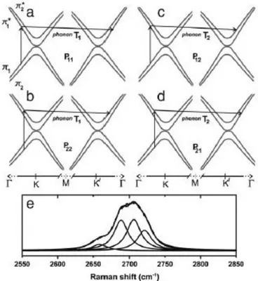
![Figure 30. Raman spectrum of a graphene edge, showing the main Raman features ref. [117]](https://thumb-eu.123doks.com/thumbv2/123dokorg/7193137.74938/53.893.260.624.387.684/figure-raman-spectrum-graphene-edge-showing-raman-features.webp)
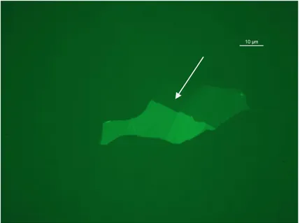

![Figure 42: The contrast image of graphene sheets on quartz substrate, ref.[139]](https://thumb-eu.123doks.com/thumbv2/123dokorg/7193137.74938/64.893.215.679.278.569/figure-contrast-image-graphene-sheets-quartz-substrate-ref.webp)