Università degli Studi di Catania
Dipartimento di Ingegneria
Elettrica, Elettronica ed Informatica
International Ph.D. in Energy
XXVII Cycle
Graphene Heterostructures
with
Wide-Bandgap Semiconductors
Gabriele Fisichella
Coordinator: Prof. Ing. L. Marletta
UniCT Supervisor: Prof. Ing. A. Raciti
IMM-CNR Supervisor: Dott. F. Giannazzo
Graphene (Gr) is a two-dimensional material constituted by an atomically thin carbon membrane, characterized by a unique combination of excellent electrical, optical, thermal and mechanical properties. Its main limitation for microelectronic applications is related to the lack of a bandgap, leading to a poor Ion/Ioff ratio when it is considered as channel
material for MOSFET devices. Novel device concepts based on Gr heterostructures with semiconductors are currently under consideration, in order to overcome these limitations. These devices are based on the vertical current transport through Gr interfaces with semiconductors or thin insulators. Their working principle exploits some unique properties of Gr, such as the atomic thickness and the field effect modulation of its workfunction. Some demonstrations of these devices, recently reported in the literature, have been based on the integration of Gr with Si technology.
This thesis work has been focused on the fabrication and the electrical characterization of high quality heterostructures of Gr with wide-bandgap semiconductors (WBS), such as Silicon Carbide (4H-SiC), Gallium Nitride (GaN) and related alloys (AlxGa1-xN), which
present superior properties for high power and high frequency electronic applications. At first, the fabrication methods have been discussed, i.e.
(i) the controlled graphitization of the surface by high temperature thermal annealing, for 4H-SiC;
(ii) a highly reproducible transfer method to move Gr, grown by CVD on copper foils, to the surface of AlGaN/GaN heterostructures.
A detailed structural, morphological and spectroscopic characterization of these Gr/WBS heterostructures has been carried out by the joint application of several analytical techniques, such as AFM; TEM, micro-Raman spectroscopy.
Secondly, the current transport mechanisms through these heterostructures have been investigated in details by properly fabricated test devices and by nanoscale resolution electrical characterization techniques (CAFM, SCM). A correlation between the nanoscale structural, morphological and electrical properties of the interfaces with the devices average electrical behavior has been achieved.
Basing on these results, some potential devices applications (such as the Gr/SiC Schottky diode with a gate modulated barrier and the hot electron transistor constituted by a Gr/AlGaN/GaN heterostructures with a Gr-base) have been discussed and their advantages with respect to the Si counterparts have been estimated.
These research activities have been carried out within the International Ph.D. course in Energy (University of Catania) and supported by the National Project PON Ambition Power (PON01_00700).
The course was organized in two main phases:
(i) the academic training, which was carried out at the Department of Electric, Electronic and Computer Engineering (DIEEI), University of Catania
(ii) the research activity, entirely carried out in the laboratories of the Institute of Microelectronic and Microsystems (IMM-CNR), Catania
In that regard, I want to thank Prof. Ing. Luigi Marletta, coordinator of Ph.D. course and Prof. Ing. Luigi Fortuna, academic training project manager. Furthermore, I would like to thank Dr. Corrado Spinella, former Director of CNR-IMM, Catania and Dr. Guglielmo Fortunato, present acting Director, for the access to the facilities of the Institute.
I would like to thank all the people who have supported and assisted me in this work.
I would like to express my gratitude at first to my Supervisor at CNR-IMM, Dr. Filippo Giannazzo, who has provided me, with great patient and care, all the essential basis on which I could build the activities described in this work.
I would like to express my thanks to my Supervisor at the University of Catania, Prof. Ing. Angelo Raciti, for his presence and his willingness.
Thanks to all the people of the team at CNR-IMM of which I was part: Dr. Fabrizio Roccaforte, who oversaw with determination the activity in its entirety, to Salvo DiFranco, who helped me with his experience to solve major practical problems in the manipulation of materials, to Dr. Raffaella Lo Nigro, who introduced me in this research field and to all the other members of the team, Dr. Patrick Fiorenza, Dr. Giuseppe Greco, Dr. Marilena Vivona, Aurora Piazza and Emanuela Schiliro, for the scientific and the moral support given to me on several occasions.
My thanks go also to other members of the CNR-IMM, Dr. Corrado Spinella, Dr. Giuseppe Nicotra and Corrado Bongiorno for the useful TEM analysis, Dr.
Thanks to the people from ST Microelectronics, Catania, for the essential support regarding materials and electrical measurements apparatus necessaries for the continuation of this activity and in particular to Dr. Sebastiano Ravesi and his team, Dr. Stella Loverso and Dr. Silvestra DiMarco, to Dr. Noemi Spartà to Dr. Cristina Tringali, to Dr. Corrado Accardi, to Dr. Ferdinando Iucolano and to Dr. Mario Saggio and his team.
Thanks to Prof. Guido G. Condorelli, and to Dr. Cristina Tudisco from the department of Chemistry of the University of Catania, for the collaboration with XPS measurements and to Prof. Simone Agnello and his team from the department of Physics of the University of Palermo, for Raman measurements.
Thanks to Ing. Mattia Frasca for the administrative support during the Ph.D. activity.
I would like to tank all the international partners, and in particular Prof. Heiko B. Weber and the members of his team, Prof. Michael Krieger, Dr. Stefan Hertel and Dr. Andreas Albert from the Chair for Applied Physics, Friedrich-Alexander University – Erlangen-Nuremberg (Germany), and Prof. Rosita Yakimova from the IFM, Linkoping University (Sweden), for their essential contributions within the framework of Gr on SiC.
Introduction 1
Chapter 1: Graphene, physical properties and production methods 7
1.1 Physical properties 7
1.2 Graphene preparation methods 21
1.2.1 Exfoliation of Graphite 21
1.2.3 Chemical Vapor Deposition of graphene on catalytic metals 22 1.2.4 Epitaxial graphene by controlled graphitization of Silicon Carbide 25
1.2.5 Graphene transfer 35
Chapter 2: Graphene heterostructures with semiconductors 43
2.1 Physics of the Gr/semiconductor junction 45
2.2 Devices based on the Gr/semiconductor junction 50
2.3 Hot electron transistors with a graphene base 53
2.4 Graphene field effect tunnelling transistors 56
Chapter 3: Fabrication of graphene heterostructures with
wide-bandgap semiconductors 59
3.1 Transfer of CVD grown graphene by electrolytic delamination and
thermo-compression printing 61
3.1.1 Description of the transfer procedure 61
3.1.2 Study of the electrolytic delamination kinetic 74
3.2.1 Fabrication of Schottky contacts on on-axis and off-axis SiC (0001) by hydrogen intercalation at epitaxial Gr/SiC interface 95
Chapter 4: Electrical characterization of graphene heterostructures with
wide-bandgap semiconductors 97
4.1 Gr/AlGaN/GaN heterostructures 97
4.1.1 Lateral current transport in Gr in contact to AlGaN 97 4.1.2 Vertical current transport in Gr/AlGaN/GaN heterostructures 99 4.1.3 From Schottky to ohmic graphene contacts to
AlGaN/GaN heterostructures: role of the AlGaN layer microstructure 116
4.2 Lateral and vertical electrical characterization
of epitaxial graphene on SiC 121
4.2.1 Lateral current transport 121
4.2.2 Vertical current transport through EG/SiC interface 130 4.3 Perspective vertical devices based on Gr/WBS heterostructures 135 4.3.1 Barristor based on the QFEG/SiC Schottky barrier 135 4.3.2 Graphene base HET based on the Gr/AlGaN/GaN heterostructure 139
Summary 145
List of Figures
Figure 1.1: allotropes of carbon represented starting from a Gr sheet (a):
(b) graphite, (c) carbon nanotubes and (d) fullerene. 7
Figure 1.2: (a) Crystal structure of monolayer Gr with A and B atoms shown as empty and full circles. The shaded rhombus is the conventional unit cell while a1 and a2 are primitive lattice vectors. (b) Reciprocal lattice of
Gr where the first Brillouin Zone is indicated with the high symmetry point Γ as the centre, K and K’ as the two non-equivalent corners and M, M’, and M’’ as the three non-equivalent centers of the edge while b1 and
b2 are reciprocal lattice vectors. 9
Figure 1.3: (a) Energy dispersion relation of the σ (red) and the π (blue) bands of the momentum |k| along the directions defined by the high symmetry points Γ, M and K. (b) Dispersion relation of Gr for the whole set of
points of the first Brillouin Zone. 10
Figure 1.4: carrier density as a function of EF - ED at a temperature T = 300 K
and (above) the variation of the EF in the Dirac cones. 12
Figure 1.5: calculated intrinsic electron mean free path (a), mobility (b) and conductivity (c) versus the carrier density n at three different temperatures (T = 10, 100 and 300 K) for a Gr sample with size
W = 1 µm × 1 µm. 15
Figure 1.6: UV–vis spectra for a different number of Gr layers, from the single layer to a four layer stack [52]. The transmitted light decreases
almost proportionally with the number of layer. 16
Figure 1.7: Phonon dispersion of Gr along high symmetry lines in the hexagonal Brillouin zone. Three Acoustic (A) and three Optical (O) phonon modes are reported. At low q, the wave vector q is linear for Longitudinal (LA) an in-plane Transverse (TA) Acoustic phonons and
Figure 1.8: Phase diagrams for the binary system (a) Ni-C and (b) Cu-C: the maximum solid solubility of C is strongly different in Ni and Cu, with ∼0.6 % at TM = 1455°C and ∼0.0076 % at TM = 1085°C for Ni and Cu
respectively. (c) and (d) illustrate the different growing mechanisms of Gr on (c) Ni where the segregation of C from bulk is the main phenomena and on (d) Cu where the surface epitaxial growth dominates.
23 Figure 1.9: SEM image of Gr domains grown on Cu before merging. Insert in
the top shows a magnification of the same domains [92]. 25 Figure 1.10: 3D illustration of the hexagonal polytype SiC which exposes two
faces with different terminations: the Si-terminated face (0001) on top
(magenta) and the C-terminated face (000-1) on the bottom (blue). 26 Figure 1.11: Schematic illustration of Gr growth: (a) subilimation of Si atoms
and reorganization of remaining C atoms in a Gr islands; (b) merging of the islands in a Gr layer and starting formation of a second Gr layer under the firs layer; (c) repetition of the same mechanism for a therd Gr
layer. 27
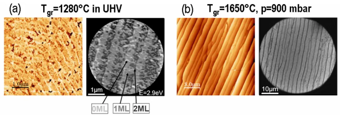
Figure 1.12: AFM morphologies and low energies electron diffraction images (left and right of each group respectively) in the cases of (a) Gr grown
in UHV at 1280°C and (b) in Ar at 900 mbar [19]. 28
Figure 1.13: LEED patterns for Gr grown on (a) the S-terminated face and on (b) the C-terminated face. Dispersion of the π-bands measured with ARPES perpendicular to the ΓK-direction of the Gr Brillouin zone for (c) a Gr single layer and (d) a double layer on the S-terminated face and
for (e) multilayer Gr on the C-terminated face. 30
Figure 1.14: temperature dependence of the Gr mobility for the case of the n-type doped Gr in the presence of the underlying buffer layer. The
mobility drop from 20 K to 300 K is more than 50% [107]. 32 Figure 1.15: Dispersion of the π-bands measured with ARPES perpendicular
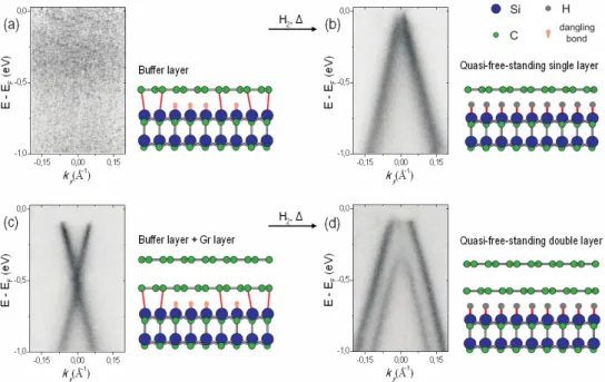
to the ΓK-direction of the Gr Brillouin zone and correspondent schematic illustration before and after the hydrogen treatment for an as grown buffer layer (a,b) and an as grown buffer layer plus a second Gr
layer (c,d) [22]. 33
Figure 1.16: temperature dependence of the Gr mobility for the case of the p-type doped Gr after the hydrogen treatment. The mobility drop from
Figure 1.17: Schematic illustration of Gr transferred from a TRT to a target
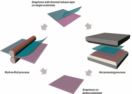
substrate by roll-to-roll or by hot pressing [121]. 38
Figure 2.1: (a) Gr and n-type semiconductor in separated systems, (b) connected in an ideal Schottky barrier without surface states and (c) considering the effect of the interfacial states. (d) Analogues representation of Gr with the p-type semiconductor in separated systems, (e) connected in an ideal Schottky barrier without surface states and (f)
considering the effect of the interfacial states. 46
Figure 2.2: qualitative atom disposal sketch (above) and schematic representation (below) of the band diagrams for the epitaxial (a) and the quasi-free-standing (b) Gr interface with 6H-SiC (0001). Large blue and small red circles represent silicon and carbon atoms of the SiC lattice respectively, grey circles represent carbon reorganized over SiC and magenta circles represent the hydrogen that passivates SiC surface. The polarization vector inside and outside of the SiC is indicated at the bottom of the figure. Circled charges represent the pseudo-charge induced by polarization. D sketches the electrostatic potential between
the SiC surface and the Gr layer [152]. 49
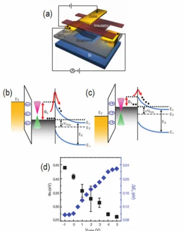
Figure 2.3: (a) A schematic diagram to show the concept of a Gr Barristor. (b-c) Schematic representation of the band diagrams of the n-type device with an applied gate bias on the top of Gr. Applying negative voltage on the gate induces holes in Gr, increasing its work function and increasing the SBH (c) while positive gate voltage decreases the SBH
(d) [9]. 52
Figure 2.4: (a) A schematic diagram to show the collector-up GB-HET structure and the common-base configuration. Gr is used as the base region for an HET structure. The purple arrows indicate the transport direction of the hot electrons. (b-c) schematic representation of the band diagrams of the device, where red arrow represent hot electrons tunnel from the silicon emitter to the Gr base through the SiO2 tunnelling
barrier. Depending on the VBE hot electrons possesses different kinetic
energy, which allows or not allows traveling over the filtering barrier.
Figure 2.5: (a) Schematic structure of Gr field-effect tunnelling transistor. (b-c) Graphic representation of the band structure for the operational principle when a Vg is applied measuring a zero bias Vb when no
tunnelling current is reached (c) and for a finite VB. (d). Tunnelling
characteristics through ~6 hBN layers measured for different Vg from
5 V to -45 V [12]. 57
Figure 3.1: (a) Optical image and (b) Raman Spectroscopy of the as-grown Gr
on Cu. 61
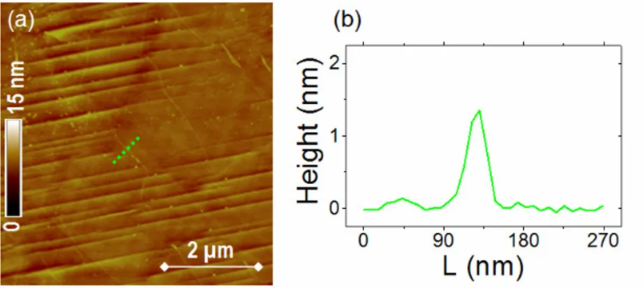
Figure 3.2: (a) AFM morphologies of as-grown Gr on Cu. A line scan perpendicular to a wrinkle of Gr on Cu is depicted and the
corresponding height profile is reported in (b). 62
Figure 3.3: (a) hot embossing NIL equipment by Karl-Suss. and (b) detail of the thermo-compressive chamber inside, consisted of thermally and mechanically controllable elements i.e. a chuck (below) and an harm
(above) . 63
Figure 3.4: (a-c) Schematic illustration of the copper planarization obtained pleasing the wrinkled copper foil (in orange) on the chuck x-y plane (a), pressing it respect to the z axes, by the arm (b) and realizing the arm pressure (c) as described by the pressure ramp in (d). (e-g) Schematic illustration of the copper attachment on a rigid substrate, obtained fishing the copper foil by the arm vacuum aspiration and aligning it above a silicon substrate (in violet) on which a double face TRT is attached (in yellow). The attachment is obtained repeating the pressure
ramp in (d). 64
Figure 3.5: (a -d) Schematic illustration of the TRT/PMMA/Gr/Cu stack preparation performed by the spin coating of Cu with PMMA (represented in blue) (a), the bake of PMMA and the contemporary release of the double face TRT (in yellow) at 150°C (b) followed by the single face TRT attachment (in magenta) on the PMMA surface, pressing the tape respect to the z axes, by the arm (c).Finally the arm releases the pressure and fishes by vacuum aspiration the final TRT/PMMA/Gr/Cu stack (d). Graphic description of the bake ramp (in magenta) followed by a pressure ramp (in black) respect to the time axis
Figure 3.6: Schematic representation of the electrolytic cell defined by a Gold foil (in yellow) working as the anode and the TRT/PMMA/Gr/Cu foil (in magenta, blue and orange respectively) working as the cathode, in a
KOH solution. 67
Figure 3.7: (a) AFM morphologiy of Gr after its separation from the metal foil (b), i.e., when it is still attached to the PMMA/TRT stack.. A line scan perpendicular to a wrinkle of Gr on PMMA is depicted in (a) and the corresponding height profile is reported in (c). A small crack in the Gr
membrane is also indicated in (a) with a circle. 69
Figure 3.8: (a-d) Schematic illustration of thermo-compressive transfer-printing process to transfer the PMMA/Gr stack (in blue) from the TRT (in magenta) (a) to the target substrate(in grey) (d), pressing it respect to the Z axes and heating by the chuck and the arm (b). Chemical elimination of PMMA to obtain a free Gr (in black) on the
target substrate (d). 70
Figure 3.9: (a-d) AFM morphologies of Gr transferred on SiO2 substrates and
(e-g) corresponding thermo-compressive ramps exploited for the transferring; (a) Gr transferred by hand, (b) Gr transferred with the high pressure and fast ramp (e), (c) Gr transferred with the optimal pressure and a fast ramp (f), Gr transferred with the final slow
thermo-compressive ramp (g). 71
Figure 3.10: (a) Set of Raman spectra collected on different positions of the Gr transferred on a SiO2 substrate, (b) plot of 2D shift and of I2D/IG for
the set of the collected positions and (c) optical image of the sampled
positions. 74
Figure 3.11: AFM morphology of Gr membranes transferred on SiO2/Si
substrates after electrolytic delamination with three different KOH concentrations: 0.05 M (a), 0.15 M (b), 0.60M (c). Histograms of wrinkles height (d), (e), (f), and distances (j), (k), (l) for the three
Figure 3.12: (a) Schematic representation (front view) of H2 bubbles
nucleation and growth at Cu perimeter: Gr wrinkle at the Cu foil perimeter (i); bubble nucleation and growth, with the deformation of the wrinkle cavity (ii); detachment of Gr from Cu (iii); coalescence of two expanding neighboring cavities (iv). (b) Schematic representation (side view) of the cavity at its maximum expansion and representation of the forces involved in the Gr delamination. (c) Measured time td for Gr
delamination from 1 cm2 Cu foil as a function of the electrolyte concentration (CKOH) and fit with the discussed microscopic model. In
the inset, the dependence of H2 supersaturation in the solution is
reported versus CKOH and fitted with the expression S = aCKOH b
. 80
Figure 3.13: Representative tAFM analyses of the bare AlGaN surface of samples A (a) and B (b). Cross-sectional TEM images of the same
samples are shown in (c) and (d). 82
Figure 3.14:Two typical tAFM images of Gr transferred to the AlGaN surface of the samples A (a) and B (b). Representative Raman spectra of Gr on
AlGaN and SiO2 (c). 83
Figure 3. 15: (a) schematic representation of the miscut angle θ formed by the SiC ingot growth axis [0001] and the vector orthogonal to the plane of cutting of the wafer. (b) 3D projection of the SiC ingot grown in the [0001] direction intersected by the plane of cutting (blue plane) with a
miscut angle θ. 85
Figure 3.16: Atomic force microscopy image of the surface morphology (a) and line profile (b) on a virgin 4H-SiC(0001) substrate cut at an angle of
8° with respect to the basal plane along the [1120] direction. 87 Figure 3.17: tAFM Surface morphology for the samples annealed at 1600 (a)
and 1700°C (b). 87
Figure 3.18: (a) 3D projection of the surface morphology of the sample annealed at 1700°C to highlight the topography of wrinkles. The blue line in (a) corresponds to the line-profile scan in (b) taken in the
direction parallel to the steps to estimate the heights of a wrinkle. 89 Figure 3.19: Typical Raman spectra measured on virgin 4H-SiC (0001) and
Figure 3.20: HRTEM of the step profile for an EG sample grown at 1700°C on 8° off axis 4H-SiC (0001) cross-sectioned perpendicularly to the [1-100] (b) Statistical distribution of the angle measured for different steps. HRTEM measures used to evaluate the number of Gr layers on
the (0001) face grown at 1600 C (c) and 1700°C (d). 91
Figure 3.21: Optical image on the O2 etched stripes in the graphitized 4H-SiC
sample by annealing at 1700°C (a). AFM height profile taken on a stripe of pristine SiC (b) and on a stripe of the sample annealed at 1700°C (c),
respectively. 92
Figure 3.22: HAADF atomic resolution STEM image of the cross sectioned profile along the [1120] direction of the (0001) surface (a) and the (11-2n) surface (b). EELS spectra and the simultaneously acquired HAADF STEM image of a faceted step in the annealed 4H-SiC sample cross-sectioned along the [1120] direction (c). Schematic cross section of the structural configuration of the 1st C layer on the faceted surface,
as deduced from STEM and EELS analyses (d). 94
Figure 3.23: schematic illustration of (a) an n+-doped 4H-SiC 3,5 off-axis with a n--doped epitaxial layer and (b) a nominally on-axis semi-insulating SiC where a nitrogen ion implantation was employed to obtain a surface n--well region and a buried n+-layer. (c) and (d) schematically illustrate the QFEG grown by thermal decomposition at 1680°C under Ar flux near atmospheric pressure followed by hydrogen intercalation at 850°C in a H2 flux, for the off-axis (c) and the on-axis
(d) samples. 95
Figure 3.24: Schematic representation of Au-capped (a) and uncapped (b) QFBLG contacts on on-axis SiC (0001) with a n--well region and a buried n+-layer obtained by nitrogen ion implantation. Schematics of Au-capped (a) and uncapped (b) QFBLG contacts on a 3.5°off-axis SiC
Figure 4.1: (a) Schematic representation of a TLM test structure fabricated on the Gr membrane residing on AlGaN. (b) I–V characteristics measured between pairs of contacts at different distances and (c) extracted resistance plotted vs. the pads distance. Analogous (d) schematic representation, (e) I-V characteristics and (f) resistance plotted vs. the pads distance for Gr residing on SiO2. From the linear fit of R versus d,
the Gr sheet resistance was evaluated. 98
Figure 4.2: Sheet resistance (Rsh) plotted vs. versus Vg from -40 V to 40 V, for
Gr residing on SiO2. 99
Figure 4.3: Two different series of I–V curves collected using an Au coated AFM tip displaced on a square array of 25 positions on AlGaN/GaN (a) and Gr/AlGaN/GaN (b). Schematic representations of the experimental setup for local I-V measurements by CAFM, in the inserts of (a) and (b). Fitting of two representative forward bias ln(I)–V curves acquired on AlGaN (c) and Gr/AlGaN (d). Conduction band diagrams of AlGaN/ GaN (e) and Gr/AlGaN/GaN heterostructures (f) with the equivalent circuit of a Schottky AlGaN/GaN diode represented as two diodes
back-to-back in series. 101
Figure 4.4: Histograms of the ΦB1, ΦB2(0) (a), and ns0 (b) obtained on an array
of 25 tip positions (spaced 1 µm from each other) on the AlGaN/GaN
and Gr/AlGaN/GaN heterostructures. 106
Figure 4.5: Behavior of ΦB1, and ΦB2(0) versus the deflection set point (DSP),
for the AlGaN/GaN and Gr/AlGaN/GaN heterostructures. 107
Figure 4.6: Behavior of ΦB1, ΦB2(0) (a) and ns0 (b) versus the metal
workfunction for the AlGaN/GaN and Gr/AlGaN/GaN heterostructures. 108 Figure 4.7: Calculated conduction band diagram for the Gr/AlGaN/GaN
heterostructure at zero bias. 109
Figure 4.8: AFM morphology (a) and phase (b) images of a region including bare AlGaN and AlGaN coated by few layers of Gr (1, 4, 5, 6 and 7 layers in a step-like fashion). (c) Height profile measured along the indicated line in (a). (d) Height values measured with respect to the AlGaN baseline level as a function of the layer number N. By linear fitting of the data, the interlayer separation (h = 0.34 ± 0.01 nm) and the
Figure 4.9: Histogram of ngr0 at the different positions in the Gr/AlGaN/GaN
heterostructure. 111
Figure 4.10: (a) Two representative C-Vtip curves measured on the
AlGaN/GaN and on the Gr/AlGaN/GaN heterostructures using an Au coated tip. In the insert, there is a schematic representation of the SCM experimental setup. (b) Electron density nsof AlGaN/GaN 2DEG as a
function of Vtip , obtained by integration of the representative C-Vtip
curves in (a). (c) Electron density ngr in Gr, as a function of Vtip. The
relation between ns and ngris shown in the insert. 113
Figure 4.11: Measured capacitance of the Gr/AlGaN/GaN heterostructure (Ctot) compared with the quantum capacitance of the AlGaN/GaN 2DEG
(CQ,ord) and the Gr quantum capacitance (CQ,gr) 114
Figure 4.12: The energy band structures of the Gr/AlGaN/GaN heterostructure at equilibrium (Vtip = 0) (a), under reverse (Vtip < 0) (b) or forward
polarization (Vtip > 0) (c). 115
Figure 4.13: I-V characteristics collected on the bare AlGaN surface of samples A (a) and B (b) and on the Gr-coated regions of samples A (c) and B (d). The fitting of representative forward bias I-V curves (with I on logarithmic scale) using the thermoionic emission model has been
reported in the insets of (a), (b) and (c). 117
Figure 4.14: Histograms of the SBH values obtained from the I-V characteristics at different tip positions on bare AlGaN (samples A and
B) and Gr-coated AlGaN (sample A). 118
Figure 4.15: (a) AFM Morphology and (b) corrispondent current map
collected for the a highly defective AlGaN surface of sample B. 119 Figure 4.16: Schematic band-diagrams for Au contacts (a) on planar AlGaN
and Au/Gr contacts (b) on planar AlGaN (solid lines) and on a V-defect
(dashed lines), where the AlGaN thickness is locally reduced. 120 Figure 4.17: Schematic representations of TLM test patterns oriented in the
direction (a) parallel ([1-100]) and (b) orthogonal [11-20] to the substrate steps. (c) Optical image of the TLM devices. Measured resistance R vs. the pad distance (d) in the two directions. The calculated
Figure 4.18: Cross-section schematics of a top-gated EG field effect transistor with channel length LG = 10 µm and channel width W = 100 µm (a). Channel conductance vs. top-gate bias and carrier density for FETs with the channel length along the [11-20] direction, i.e. orthogonal to the SiC steps, and the [1-100] direction, i.e. parallel to the SiC Steps (b). Calculated mobility µ in the electron branch for FETs with the channel
length along [11-20] and [1-100] directions (c). 123
Figure 4.19: Surface morphology (a) and the corresponding current map (b) measured by CAFM on the as-grown EG/4H-SiC(0001) sample. Line-profiles of the height (c) and of the current (d) along the indicated
directions in the maps. 124
Figure 4.20: 3D projection of the surface morphology measured in a region nearby a 200 nm-thick Ni/Au contact onto EG(a). High resolution morphology (b) and resistance map (c) obtained by CAFM in the 100 nm × 100 nm region indicated in (a) by the circle. Line-scan taken in the direction perpendicular to the steps (d), indicated by the horizontal arrow in (c). Line-scans taken in the direction parallel to the steps along (11-2n) and (0001) faces (e), as indicated by the vertical
black and red arrows in (c). 125
Figure 4.21: Histograms of the REG values, obtained on 20 different terraces
and facets within the EG sample. 126
Figure 4.22: Histogram of the local mean free path distribution in EG grown
on 8°off axis 4H-SiC (0001) by annealing at 1600 C. 129
Figure 4.23: Representative I-V characteristics measured on Au capped QFBLG contacts to SiC with 10 µm (a) and 1 µm diameter (b). AFM
morphologies of the contacts are shown in the inserts. 131 Figure 4.24: Dependence of the measured SBH on the contacts diameter for
QFBLG contacts fabricated on SiC substrates with large (a) and small
terraces (b). 132
Figure 4.25: CAFM morphology (a,c) and current map (b,d) on uncapped QFBLG-SiC contacts to on on-axis SiC (upper images) and 3.5°
Figure 4.26: (a) Dependence of the ideality factor on the contacts diameter for QFBLG contacts fabricated on SiC substrates with small terraces. (b) plot of the ideality factor vs. the correspondent SBH. The red line is the linear fit which indicates that when n tends to the unity the SBH
approximate the value ~1.6 eV. 134
Figure 4.27: (a) schematic cross section of a QFEG/SiC vertical Barristor and
(b) expected behavior of ΦBvs. Vg. 135
Figure 4.28: (a) forward bias Ids - Vds characteristics for different values of Vg
and (b) Ids - Vg transcharacteristics for different Vsd voltages calculated
for a barristor based on the QFEG/SiC Schottky barrier. 137 Figure 4.29: (a) schematic cross section of a Gr/Si vertical Barristor,
considering an ideal Gs/Si interface obtainable by hydrogen passivation
of the Si surface. (b) Expected behavior of ΦBvs. Vg for this device. 137
Figure 4.30: (a) forward bias Ids - Vds characteristics for different values of Vg
and (b) Ids - Vg transcharacteristics for different Vsd voltages calculated
for a Barristor based on the Gr/Si Schottky barrier. 138
Figure 4.31: Schematic representations of the cross-section (a) and of the top-view (b) of a Metal/Al2O3/Gr/AlGaN/GaN HET where the AlGaN
layer works as the emitter-base barrier, the 2DEG at AlGaN/GaN
interface as the emitter and Gr as the base. 140
Figure 4.32: energy band diagram of the Metal/Al2O3/Gr/AlGaN/GaN HET:
for Veb = 0 and Vbc = 0 (a), for Veb > 0 and Vbc = 0 and finally for Veb > 0
and Vbc > Φbc0 - Φeb0, when an Ic is observed for Fowler-Nordheim
tunneling across an affective barrier Φ≈Φbc0 - Veb (c). 140
Figure 4.33: estimated plot of the Ib injected in the base as a function of Veb (a).
The calculated Ic plotted as a function of Veb for various values of Vbc
(b) and vice versa as a function of Vbc for various values of Veb (c). A
strong dependence of the Ic from the Vbc bias is clearly visible. 142
Figure 4.34: comparison between the emitter current (Ie), the current injected
in the base (Ib) and the collector current (Ic) plotted vs. the Vbe for a
List of Tables
Table 1.1: Main physical properties of Gr and possible applications. 20
Table 3.1: physical properties of Si, 4H-SiC and GaN [169]. 59 Table 3.2: Time (td) required to obtain the complete delamination of Gr from
Acronyms
2DEG two-Dimensional Electron Gas
4H-SiC Hexagonal polytype 4H Silicon Carbide AC-STEM Aberration Corrected Scanning TEM AFM Atomic Force Microscopy
AlGaN/GaN Aluminum Gallium Nitride/Gallium Nitride
ARPES Angle-Resolved inverse PhotoEmission Spectroscopy CAFM Conductive Atomic Force Microscopy
C-V Capacitance-Voltage CVD Chemical Vapor Deposition DC Direct Current
EELS Electron Energy Loss Spectroscopy EG Epitaxial Graphene
FET Field Effect Transistor FWHM Full Width at Half Maximum
GB-HET Graphene Base Hot Electron Transistor Gr Graphene
HAADF High Angle Annular Dark Field hBN hexagonal Boron Nitride HET Hot Electron Transistor
HOPG High Oriented Pyrolytic Graphite HRTEM High Resolution TEM
LEED Low Energy Electron Diffraction
MOCVD Metal Organic Chemical Vapor Deposition
MOSFET Metal-Oxide-Semiconductor Field-Effect Transistor NIL Nano-Imprint Lithography
PDMS PolyDiMethylSiloxane
PECVD Plasma-Enhanced Chemical Vapor Deposition PMMA Poly(Methyl MethAcrylate)
QFBLG Quasi-Free-standing BiLayer Graphene QFEG Quasi-Free-standing Epitaxial Graphene RMS Rout Mean Square
SBH Schottky Barrier Height
SCM Scanning Capacitance Microscopy
STEM Scanning Transmission Electron Microscopes tAFM tapping mode Atomic Force Microscopy TEM Transmission Electron Microscopy TLM Transmission Line Model
UHV Ultra High Vacuum v. d. W. van der Waals
WBS Wide-Bandgap Semiconductor XPS X-ray Photoemission Spectroscopy
Graphene [ 1 ] (Gr) is a two-dimensional (2D) sheet of C atoms with sp2 hybridization. It is currently one of the most investigated topics in condensed matter physics, with an exponential growth in the number of scientific papers (but also patent applications) published yearly on this subject. In only ten years from the first pioneering experiments by Geim and Novoselov [ 2 ], the research on Gr evolved into several branches, addressing different potential applications of this material, including electronics, optoelectronics, spintronics, nanomechanics, magnetism, chemistry, nanomedicine and so on. Furthermore, this research field covers nowadays an entire class of (2D) materials, including chemical derivatives of Gr (such as the graphene oxide, graphane, fluorographene,…), boron nitride, transition metal dichalcogenides (MoS2, WS2, MoSe2, WSe2,..), topological
insulators, silicene, germanene, phosphorene, [3]…
The strong interest of the scientific community on Gr is mainly due to the unique combination of excellent electrical [ 4 ], optical [ 5 , 6 ], thermal [ 7 ] and mechanical [8] properties in this atomically thin material, which pave the way to several applications in different fields.
In particular, the excellent carrier mobility (> 105 cm2V-1s-1 under “ideal” conditions and 104 - 105 cm2V--1s-1 in “ordinary” conditions), the carrier density modulation by field effect [9,10,11,12], the excellent thermal conductivity, the optical transparency (∼97.3% for a monolayer of Gr) and the mechanical flexibility, make Gr a material of choice for some applications in electronics, such as RF devices, optoelectronics, photovoltaics, flexible electronics.
The main limitation of Gr for electronic applications is represented by the “zero-bandgap”, which results in a low ratio between the on- and off-state currents when Gr is used as a channel material in a conventional Metal-Oxide-Semiconductor Field-Effect Transistor (MOSFET) architecture. Several studies have been performed in the last years with the aim to open a bandgap in the Gr band structure, either by quantum confinement effects in Gr nanoribbons lithographically defined from 2D Gr, or by proper chemical modification (hydrogenation, fluorination,..) of Gr. In most of the cases, the observation of a bandgap was accompanied to a strong degradation of Gr mobility, i.e. to losing one of the main advantages of Gr.
Currently, two main trends emerged for Gr used in electronics:
(i) Replacing Gr with other semiconducting 2D materials (such as MoS2) in the
channel of MOSFETs devices, and using Gr for interconnects or as a source/drain or gate contact;
(ii) Employing Gr as active material in new device architectures (i.e. different from MOSFET), where some of its peculiar physical properties (atomic thickness, field effect modulation of workfunction, low density of states…) can be profitably used. These alternative device concepts (more extensively discussed in the following) are mainly based on heterostructures of Gr with semiconductors or insulating materials.
Due to the unavailability of high quality semiconducting 2D materials on large area, the first approach is currently pursued only on explorative basis.
On the other hand, the second solution can take benefit of the huge progresses in the synthesis of high quality Gr on large area during the last 10 years, in particular by Chemical Vapor Deposition (CVD) on catalytic metals or by controlled graphitization of the silicon carbide (SiC) surface. Obviously, the fabrication of heterostructures of Gr with semiconductors or insulators requires significant efforts aimed at the integration of these materials.
It is well known how Gr electronic properties (carrier density, mobility) are strongly affected by the interaction with the underlying substrate. To date, many of the efforts have been directed to minimize the effect of such interactions in order to preserve as much as possible the outstanding “in plane” transport properties of Gr, to be used as a high mobility conductor in “lateral” devices.
On the other hand, a deeper understanding of the current transport phenomena through Gr/semiconductor or Gr/insulator interfaces are highly required to adequately describe the working principle of the above mentioned “vertical” devices, based on Gr heterostructures.
This thesis work is focused on the fabrication of high quality heterostructures of Gr with Wide-Bandgap Semiconductors (WBS), such as Silicon Carbide (SiC) [13], Gallium Nitride (GaN) and related alloys (AlxGa1-xN) [ 14,15, 16 ], and on the
investigation of current transport at these interfaces. SiC and GaN are, to date, the most technologically relevant and strategic materials for high power, high frequency and energy efficient electronics. In particular, SiC plays a major role in the fabrication of Schottky diodes and MOSFETs, for high power applications (already commercially available in the range of 600 - 1200 V), whereas GaN-based
power and high frequency applications, taking advantage of the high mobility two dimensional electron gas (2DEG), which is spontaneously formed at the interface between AlGaN and GaN in AlxGa1-xN/GaN heterostructures [14,17].
Hence, the motivation of this work is to exploit Gr in junction with these WBSs, taking advantage from their peculiar electronic properties, such as the high critical electric field and the presence of a 2DEG at AlxGa1-xN/GaN interface. This can
result in the demonstration of novel electronic device concepts or in the introduction of new functionalities in existing SiC and GaN devices.
SiC is particularly interesting for the fabrication of heterostructures with Gr, since Gr can be directly grown on its surface by controlled graphitization during high temperature thermal treatments. SiC polytype, crystalline orientation and wafer miscut angle strongly influence Gr growth. In particular, using the (0001) face of the hexagonal polytypes (4H or 6H), monolayer or few layers of Gr epitaxially oriented with respect to the substrate are obtained, with highly homogeneous coverage also on wafer scale [18,19,20]. Due to these peculiar qualities, Gr on SiC has been widely investigated in the last years. Gr provides a high-mobility 2DEG suitable for low power RF devices fabrication on SiC surface [21]. Furthermore, it is very interesting also as a contact to SiC, since excellent quality ohmic or Schottky contacts can be obtained by properly tailoring the atomic structure of Gr/SiC interface [22,23]. However, much remains to understand about the impact of SiC peculiar morphology both on the lateral current transport in the Gr sheet and on the vertical current transport through the Gr/SiC interface [24].
Gr integration with GaN has been recently considered, both for optoelectronic applications (i.e., as a transparent conductor in GaN LEDs [25]), and as a heat dissipation element for thermal management in power High Electron Mobility Transistors (HEMTs) [26]. Probably, a limiting factor in this case is the difficulty to grow Gr directly on the GaN surface. Therefore, in order to have a Gr single sheet over a sufficiently large area, suitable for electronic applications, a transfer procedure must be adopted to move the Gr membrane from the growth substrate (typically copper) to GaN. This is a critical step for the final quality of the heterostructure.
In my Ph.D. activities, the following experimental issues have been addressed: (i) The fabrication and the high-resolution structural and morphological
characterization of high quality Gr heterostructures with 4H-SiC (0001) and AlxGa1-xN/GaN;
(ii) The electrical characterization of transport properties through these Gr/semiconductor interfaces, employing advanced nanoscale-resolved characterization techniques (conductive atomic force microscopy and scanning capacitance spectroscopy), in order to correlate the local structural and electrical properties.
This thesis is organized in four chapters, as follows:
In Chapter 1, an overview of the Gr general physical properties and of the state-of-the-art Gr production methods is provided. Particular attention will be paid to the two main large-area growth methods, i.e. the CVD growth on catalytic metals and the controlled graphitization of SiC. The current transfer methods to move Gr from the metal foil to an arbitrary target substrate will be discussed in details, since it represents a critical step for the final quality of Gr.
In Chapter 2, an overview of the literature results on Gr heterostructures with semiconductors and/or insulators is reported. In particular, the basic physics of Gr/semicondutor contacts will be introduced. Furthermore, an introduction will be provided on the device concepts based on Gr heterostructures reported to date in the literature, i.e. (i) the Gr/Si Schottky diode with a gate modulated barrier (Barristor), (ii) the Hot Electron Transistor (HET) with a Gr base, and (iii) the field effect modulated tunnel devices.
In Chapter 3 is illustrated the experimental activity on the fabrication of Gr heterostructures with AlxGa1-xN/GaN and with 4H-SiC. A highly reproducible
transfer method has been developed to move Gr grown by CVD on copper foils to the final substrate. This approach was based on some innovative solutions, such as the electrolytic delamination process to separate Gr from the copper foil [27] and a thermo-compressive transfer printing of the delaminated Gr on the target substrate. These solutions can have significant potential impact in the industrialization of Gr transfer procedure. Differently than the typical transfer approach (where Gr is separated from Cu by chemical etching of this metal), this method preserves Cu, making it available for an unlimited number of CVD growth cycles. This would reduce both the production costs and the environmental impact, in the perspective of a process scale-up. Furthermore, it potentially eliminates Cu contaminations on Gr, which can hinder its integration in semiconductor fabs. The use of thermo-compression printing (based on the hot embossing nanoimprint lithography technology) allows a highly reproducible stamping of delaminated Gr on the desired substrate position.
This transfer method was demonstrated to be valid to transfer Gr on several substrates (including Si, SiO2, SiC, GaN,…).
In particular, it has been employed to fabricate Gr heterostructures with AlGaN/GaN, obtaining a uniform Gr coverage on AlGaN layers with different morphologies, i.e. on flat and defects rich ones.
Gr heterostructures with SiC were obtained by the controlled graphitization of the surface during high temperature (1600 – 1700°C) thermal treatments. The effect of the annealing temperature and of the wafer miscut angle on the number of Gr layers was accurately investigated using different characterization techniques (including Atomic Force Microscopy, Transmission Electron Microscopy, micro-Raman spectroscopy). The atomic scale structural properties of Gr interface with SiC surface were investigated by atomic resolution scanning transmission electron microscopy, revealing peculiar difference between local structure on (0001) terraces and (11-2n) facets of SiC. [28,29].
In Chapter 4, a detailed electrical characterization of the fabricated Gr heterostructures with 4H-SiC and AlxGa1-xN/GaN will be reported. Firstly, the
lateral current transport in Gr residing on these two substrates was investigated on properly fabricated test devices, extracting characteristic Gr electrical properties such as the sheet resistance, carrier density and mobility. Therefore, the vertical current transport through the Gr/semiconductor interfaces was extensively investigated. In particular, advanced nanoscale electrical measurements (Conductive Atomic Force Microscopy and Scanning Capacitance Microscopy) were employed to this aim to get an insight on the lateral uniformity of the contact. In the case of Gr onto AlGaN/GaN heterostructures, the vertical current transport mechanisms, and in particular the role of the AlGaN surface states and the impact of the AlGaN layer microstructure were properly investigated observing the possibility to have a low Schottky Barrier Height (SBH) [30]or even to convert the rectifying contact in an ohmic contact. [31].
In the case of Gr on 4H-SiC (0001), a peculiar anisotropy of the lateral current transport in Gr was observed and related to the peculiar morphology of SiC substrate, which exhibits parallel steps originating from the wafer miscut angle [28,29].
The vertical current transport through the Gr/SiC heterostructure allowed to elucidate the impact of the interface atomic structure on the Gr electronic properties [32]. It is worth noticing that an ohmic behavior is typically observed for
Conversely, a rectifying (Schottky) contact (with a barrier height of 0.9 – 1 eV measured by Current-Voltage (I-V) analyses and ∼1.5 eV measured by Capacitance-Voltage (C-V) analyses, respectively) was obtained after passivation of the interface between Epitaxial Graphene (EG) and SiC by a post-growth hydrogen intercalation. The ohmic behavior in the as-grown epitaxial Gr depends on the presence of an interfacial C layer (the buffer layer) partially covalently bonded with the Si face of SiC. The charged Si dangling bonds at the interface cause a high n-type doping of the overlying Gr and a low SBH (∼0.3 eV), resulting in an ohmic contact. This is converted into a Schottky contact by the hydrogen intercalation, which causes a decoupling of the aforementioned buffer layer from the Si face (i.e. its conversion into a Quasi-Free-standing Epitaxial Gr layer) and the saturation of the interfacial Si dangling bonds [22,23]. Nanoscale resolution I-V characterizations by Conductive Atomic Force Microscopy (CAFM) clarified some peculiar electrical properties of the hydrogen intercalated Gr/SiC heterostructure, such as locally reduced SBH at Gr interface with (11-2n) facets, which can explain the discrepancy between the macroscopically evaluated Schottky barriers by I-V and C-V analyses.
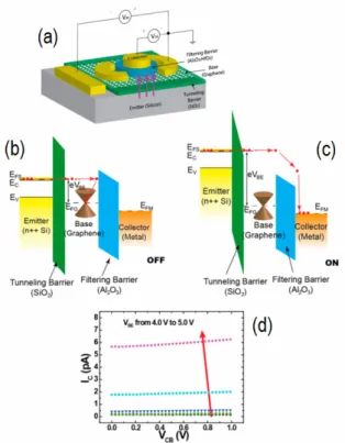
Basing on this understanding of the current transport mechanisms at Gr/SiC and Gr/AlGaN/GaN heterostructures, some of the possible devices applications will be discussed. In particular, the performance of a Barristor based on Gr Schottky contacts to SiC will be evaluated and compared with those of a similar device structure based on Gr contacts to silicon. Significant advantages in terms of lower current dissipation in the off-state and of superior breakdown voltage are expected in the case of epitaxial Gr Schottky contacts to SiC.
The potential applications of Gr/AlGaN/GaN heterostructures will be discussed, as well, like a HET where the 2DEG at AlGaN/GaN interface works as the emitter, Gr works as a base and the AlGaN barrier layer works as emitter-base barrier. The advantages of this device structure will be discussed with respect to Gr-base HET devices with Si emitter and SiO2 emitter-base barrier.
production methods
1.1 Physical properties
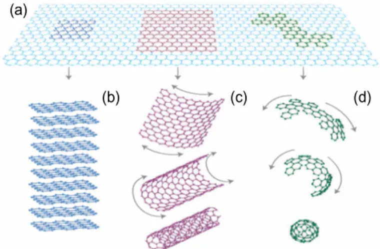
Gr is a crystalline allotrope of carbon, consisting of a two-dimensional (2D) layer of atoms packed in a honeycomb lattice (see Figure 1.1 (a)). It represents the basic structure for other allotropes of carbon of all other dimensionalities: the 3D graphite, formed by a sequence of stacked Gr layers (Figure 1.1 (b)), the 1D nanotubes, described as rolled Gr [33] (Figure 1.1 (c)), the 0D fullerene, described as wrapped Gr [34,35] (Figure 1.1 (d)). (a) (d) (b) (c) (a) (d) (b) (c)
Figure 1.1: allotropes of carbon represented starting from a Gr sheet (a): (b) graphite,
(c) carbon nanotubes and (d) fullerene.
From a molecular point of view, Gr can be also suitably described as an indefinitely extended polycyclic aromatic molecule. Each C atom in the hexagonal Gr lattice forms σ-bonds with three adjacent C atoms by the overlapping of sp2 hybridized molecular orbitals in a trigonal planar geometry on the xy-plane and mutual 120° angles. In this configuration, for each C atom a single not hybridized
preserved. The energy distribution of molecular orbitals in an aromatic system can be calculated by the Linear Combination of Atomic Orbitals (LCAO) method. Within this approach, the linear combination of a number N of 2pz orbitals
generates an equal number of molecular orbitals: N/2 are totally filled π-bonding orbitals at lower energies and N/2 are totally empty π* anti bonding orbitals at higher energies. The electrons in these π and π* orbitals are completely delocalized over the aromatic system. As a consequence, the C-C distance of 0.142 nm for each pair of nearest-neighbor C atoms is roughly the average length of a single (0.154 nm) and a double bond (0.134 nm), which is a scenario that is analogous to that of benzene described by Pauling since 1931 [36].
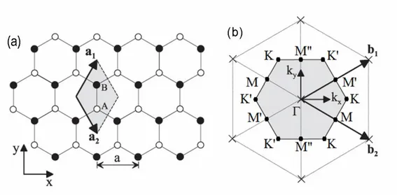
Looking at Gr as an indefinitely extended 2D crystal, the problem of energy band structure calculation can be addressed solving the Schrodinger equation for the electrons in the Gr hexagonal lattice in the tight-binding approximation [37]. The Gr structure, which is not a Bravais lattice because of the non-equivalence of neighboring sites, can be divided in two sub-lattices A and B, as indicated in Figure 1.2 (a) by full and empty circles respectively, in order to satisfy the equivalence conditions to define Bravais lattices. Consequentially grouping two neighboring carbon atoms (one for each sub-lattice) in a single basis, a triangular Bravais lattice is rigorously defined.
The basis lattice vectors a1 and a2 (see Figure 1.2 (a)) can be defined as:
) 3 , 3 ( 2 1 a a = , 2 = 2(3,− 3) a a (1.1)
where a is the C-C distance which is exactly 0.142 nm in the case of Gr.
Considering the Gr reciprocal lattice in the momentum space, the corresponding basis vectors b1 and b2 are:
) 3 , 1 ( 3 2 1 a b = π , (1, 3) 3 2 2 = − a b π (1.2)
Figure 1.2: (a) Crystal structure of monolayer Gr with A and B atoms shown as
empty and full circles. The shaded rhombus is the conventional unit cell while a1 and
a2 are primitive lattice vectors. (b) Reciprocal lattice of Gr where the first Brillouin
Zone is indicated with the high symmetry point Γ as the centre, K and K’ as the two non-equivalent corners and M, M’, and M’’ as the three non-equivalent centers of the edge while b1 and b2 are reciprocal lattice vectors.
In Figure 1.2 (b) the first Brillouin Zone of the Gr reciprocal lattice is indicated with the high symmetry point Γ as the centre, K and K’ as the two non-equivalent corners and M, M’, and M’’ as the three non-equivalent centers of the edge.
The K and K’ high symmetry points are especially interesting because of the very peculiar shape of the conduction and the valence bands close to these point, as it will be discussed in the following.
The energy bands obtained from the solution of the Schrödinger equation in the tight-binding approximation can be expressed as:
) ( 3 ) (k t f k E =± + ± (1.3) Where f(k) is a function of the momentum k and t is the hopping energy (t ≈ 2.8 eV estimated by ab initio calculations [38]), defined as the energy required for an electron to hop from a C atom to the three nearest-neighbors atoms. The positive or the negative signs in Equation (1.3) refer to the upper antibonding band (π*) and the lower bonding band (π) respectively.
In Figure 1.3 (a) the calculated valence and the conduction band energies are plotted as a function of the momentum |k| along the directions defined by the high symmetry points (e.g. Γ, M and K) of the first Brillouin Zone. The energy difference between the conduction and valence band is maximum in correspondence with the Brillouin zone centre Γ, whereas it is null (zero band gap) in the K an K’ corners of the the Brillouin zone, where the valence band maximum and conduction band minimum merge in the singularity points D and D’, called Dirac points (see Figure 1.3 (b)).
Figure 1.3: (a) Energy dispersion relation of the σ (red) and the π (blue) bands of the
momentum |k| along the directions defined by the high symmetry points Γ, M and K. (b) Dispersion relation of Gr for the whole set of points of the first Brillouin Zone.
Considering that for neutral Gr the chemical potential (i.e. the Fermi energy EF) is
coincident with the Dirac points (D and D’ for K and K’ respectively), it is relevant to calculate the dispersion relations close to K (or K’).
For this porpoise, the wavevector k can be expressed as k = K + k’, where K is the wavevector of the K point (with the origin in the Brillouin zone center) and k’ is a wavevector with the origin in the K point. Close to the K point, i.e. for |k’| << |K|, Equation (1.3) can be expanded using the Taylor series and approximated as [37]:
( )
k' v k'E ≈±h F
± (1.4)
Where vF is the Fermi velocity, defined as vF = 3ta/2ħ, with a value vF≈ 10 6
m/s.
It is worth noting that this linear dispersion relation for electrons in Gr is different from the usual parabolic relation:
( )
m k k E 2 2 2 h = (1.5)For electrons in semiconductors, where the electron velocity is:
m
E
m
k
v
=
/
=
2
/
(1.6)The above linear dispersion resembles that of massless particles (such as photons) or that of ultra-relativistic particles, with the exception of the Fermi velocity value which is vF≈ c/300 lower than the speed of light c = 3×10
8
m/s.
The linear dispersion relation in Gr has been experimentally verified in different ways. The most direct approach is using angle resolved photoemission spectroscopy, which is able to simultaneously probe the energy and wavevector of photoemitted electrons with energy below the Fermi level.
Many of the peculiar electronic properties of Gr, such as the density of electronic states linearly depending on the energy and the ambipolar current transport, are a direct consequence of the linear dispersion relation.
The density of electronic states (ρ) in Gr can be calculated starting from the dispersion relation [37,39]. Clearly, close to the Dirac point (E = 0) it is a linear function of the energy E:
| | 2 ) ( 2 2 E v g g E F v s h
π
ρ
= (1.7)Where gs = 2 and gv = 2 are the spin and valley degeneracy, respectively. This
dependence of the density of states on the energy for Gr has strong implications both on the electronic and optical properties of Gr. As an example, it means that, changing the Fermi energy from the Dirac point to EF by the application of an
external electric field, only a limited number of states are available to be occupied by electrons at that fixed value of EF. This makes Gr very different from common
metals, for which the density of electronic states at the Fermi level is so high to accommodate all the electrons induced by the electric field. Because of that, while a thin metal film is able to screen completely an electric field to penetrate through it, a Gr membrane causes only a partial screening.
For a fixed value of the Fermi energy, the carrier density in Gr can be expressed as:
( ) ( )
∫
∞
= E f EdE
Where ρ(E) is the density of states and
( )
− + = kT E E E f F exp 1 1 (1.9)Is the Fermi distribution. A plot of the carrier density as a function of EF - ED at a
temperature T = 300 K is reported in Figure 1.4 The majority carriers are electrons when EF - ED > 0 (Fermi level in the conduction band) and holes when EF - ED < 0
(Fermi level in the valence band). Noteworthy, even at the neutrality point (EF = ED), where the density of states is zero, a finite value of the carrier density
2 10 2 10 5 , 6 6 − × ≈ = = cm v T k p n F B i i h π (1.10)
is found, due to thermal agitation effects.
Figure 1.4: carrier density as a function of EF - ED at a temperature T = 300 K and
(above) the variation of the EF in the Dirac cones.
On the basis of these properties it is relevant a direct comparison between Gr and a conventional 2DEG, that can be found in the channel region of MOSFETs (in the inversion regime) or at the heterointerface of semiconductor heterostructures (such as AlGaAs/GaAs, AlGaN/GaN,…).
Gr actually deserves the definition of 2DEG in the strictest sense of the word because of the real confinement of the electron gas within its atomically thick dimensionality. A conventional 2DEG is instead confined in a thin bulk region, with a thickness in the order of 1 – 10 nm depending on the material and the electron confinement mechanism. Electrons confined in a thin sheet can be defined as a 2DEG when the thickness t of this region is smaller than the Fermi wavelength λF.
Considering that the expression of the Fermi wavelength is
n kF
F 2
π
/ 2π
/λ
= = (1.11)t < λF for Gr is always satisfied even if unphysically large n = 10
14
cm-2 is considered.
The 2D electron nature of Gr was immediately clarified since the first experiments on this material [2,40] by the observation of the quantum Hall effect, which is the straightest demonstration to reveal 2D electron phenomenon. However, an unconventional quantization of Hall conductivity as a function of the carrier density was found for a single layer of Gr with respect to that previously observed in other 2DEGs. This is a consequence of the linear, Dirac-like, spectrum of quasiparticle excitations of Gr and by “pseudospin” degeneracy associated to the presence of two carbon sublattices [41].
The main effective differences between Gr and a traditional 2DEG are related to the transport properties. The linear dispersion relation for Gr close to the Dirac points remains valid for electron energies |E| < 1 eV. These energy range is large enough with respect to the thermal excitation energy (kBT) to allow the observation
of many electronic properties deriving from this peculiar band-structure even at temperatures as high as 300 K (i.e. room temperature) [42].
In general, the experimental quantity that is measured during current transport measurements is the conductivity σ, which is related to the carrier mobility µ and to the electron density n as
µ
σ
=qn (1.12)Being q is the electron charge.
Under ideal experimental conditions, such as for free-standing [4] or boron nitride encapsulated Gr [ 43 , 44 , 45 ], giant carrier mobility was observed, i.e.
µ > 106 cm2V-1s-1 at low temperatures and µ ≈ 105
The relation between the mobility and the electron mean free path l can be obtained by a semi-classical approach based on the Boltzmann transport theory and the relaxation time approximation [46,47], as
n ql n qvF
π
π
τ
µ
h h = = (1.13)where τ is the relaxation time for a fixed value of Fermi energy.
From this relation it is clear that the limiting factors for the electron mobility of Gr are directly related to the scattering mechanisms, which limit the electron mean free path.
Under nearly ideal conditions which allows Gr to be considered as a defect-free planar sheet without any contamination or environmental influence, the solely limiting factor for the electron mean free path is the scattering of longitudinal acoustical phonons (lAD,Phon), inversely proportional to the electron density and to
the temperature T as 2 / 1 2 2 2 2 , − ≈ n T k D v v l B A F s gr Phon AD π ρ h (1.14) where ρgr≈ 7.6 x 10 -7
kg m-2 [48] is the Gr mass density, DA≈ 18 eV [48] is the
acoustic deformation potential, vs≈ 2.1 x 10
4
m s-1 is the acoustic phonons group velocity and kB is the Boltzmann constant.
Under proper experimental conditions, it is possible to approach the theoretical phonon-scattering limit, even at room temperature. As illustrated in Figure 1.5, the expected electron mean free path (Figure 1.5 (a)), mobility (Figure 1.5 (b)) and conductivity (Figure 1.5 (c)) plotted vs. the carrier density are calculated at different temperatures for a micrometric Gr sample. A lAD,Phon higher than the
device size (typically in the order or 1 µm or below) is actually obtainable at low-temperatures, allowing the observation of ballistic current transport without any energy dissipation [45].
Figure 1.5: calculated intrinsic electron mean free path (a), mobility (b) and
conductivity (c) versus the carrier density n at three different temperatures (T = 10, 100 and 300 K) for a Gr sample with size W = 1 µm × 1 µm.
Under practical experimental conditions, e.g. at room temperature and under ambient environment, the mobility as well as the electron mean free path of Gr can be significantly reduced due to several effects. Gr is very sensitive to the interaction with the substrate and with the external environment. Furthermore, mobility can be strongly dependent on the Gr synthesis method (polycristallinity, defects and deformations, chemical modifications) and on the subsequent manipulation processes (e.g. the Gr transfer procedure) and/or on any additional processes for devices fabrication, which can introduce structural and morphological damages or chemical residues. Typical mobility values of Gr devices reported in the literature can range from ~102 cm2V-1s-1 to ~104 cm2V-1s-1 at room temperature and under ambient environment.
The most common “extrinsic” scattering mechanisms, which reduce the electron mean free path in Gr are: (i) the scattering by charged impurities [49], which can be localized on top of Gr or at the interface between Gr and the substrate; (ii) the resonant scattering [50] due to Gr lattice defects (e.g. vacancies) or to various organic groups covalently bonded in place of C-C double bonds [51].
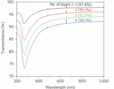
The peculiar electronic structure of Gr is reflected not only in the electrical properties but also on the optical ones, in particular in the absorption and transmission of light. Noteworthy, the optical absorption of a monolayer is quite constant (∼2.3%) over the entire spectrum of visible wavelengths, covering also part of the UV and the IR band, as illustrated in Figure 1.6. Furthermore, the absorbance of a few-layers of Gr stack increases proportionally to the number of layers (for N up to 4) [52,5].
Figure 1.6: UV–vis spectra for a different number of Gr layers, from the single layer
to a four layer stack [52]. The transmitted light decreases almost proportionally with the number of layer.
As a consequence of the linear dispersion relation of Gr around the Dirac point, the optical conductance G (related to the optical inter-band transitions) results to be independent on frequency in a broad range of photon energies and corresponds to the universal optical conductance G0 [53]:
1 5 2 0 6.08 10 2 ) ( = ≡ ≈ × − Ω− h e G Gω π (1.15)
This constant behavior of G with the photon frequency implies that other observable quantities such as the optical transmittance T, the absorbance A and the reflectance R are frequency independent as well.
For a freestanding Gr monolayer T, R and A can be expressed applying the Fresnel equations in the thin-film limit, in the form:
% 7 . 97 1 ) 5 . 0 1 ( ) / 2 1 ( + 2 = + 2 = − = ≡
π
G c −πα
−πα
T (1.16) % 1 . 0 25 . 0 2 2 < ≡ T Rπ
α
(1.17)%
3
.
2
1
−
=
=
T
A
(1.18) Where: 137 / 1 / 2 2 ≈ =π
e hcα
(1.19)is the fine structure constant.
The remarkable optical absorption of Gr was the key property that allowed the easy identification of single layers of this material in the first pioneering works of by Geim and coworkers. In fact, transferring Gr over a Si substrate capped with SiO2
of appropriate thickness (∼100 nm or ∼300 nm), it is possible to achieve a significant optical contrast between regions coated and uncoated with Gr [54,55]. Despite its high absorbance (in relation to its atomic thickness), in absolute terms Gr can be considered as an excellent transparent conductor. It is currently investigated as a replacement of ITO for applications in optoelectronics (light emitting diodes [25,56]) and photovoltaic (new generation solar cells [57]). Due to its high flexibility, it is the ideal candidate for flexible and organic light emitting devices [58].
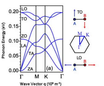
In addition to the electronic band-structure, also the phononic dispersion relation has very important implications on some physical properties of Gr such as the thermal conductivity and the specific heat.
Gr exhibits an in-plane thermal conductivity among the highest of known material, ranging from 2000 to 5000 W m−1K−1 [7,59,60 , 61 ] for suspended single layer membranes, at room temperature, in contrast with the thermal conductivity along