Alma Mater Studiorum · Universit`
a di
Bologna
SCUOLA DI SCIENZE
Corso di Laurea Magistrale in Informatica
MaldOS:
a Moderately Abstracted Layer for
Developing Operating Systems
Relatore:
Chiar.mo Prof.
Renzo Davoli
Presentata da:
Mattia Maldini
Sessione III
Anno Accademico 2018-2019
Abstract
The course of Operating Systems is arguably one of the most crucial part of a computer science course. While it is safe to say a small minority of students will ever face the challenge to develop software below the OS level, the understanding of its principles is paramount in the formation of a proper computer scientist. The theory behind Operating Systems is not a particularly complex topic. Ideas like process scheduling, execution levels and resource semaphores are intuitively grasped by students; yet mastering these notions through abstract study alone will prove tedious if not impossible. Devising a practical - albeit simplified - implementation of said notions can go a long way in helping students to really understand the underlying workflow of the processor as a whole in all its nuances.
Developing a proof-of-concept OS, however, is not as simple as creating software for an already existing one. The complexity of real-world hardware goes way beyond what students are required to learn, which makes hard to even find a proper machine architecture to run the project on.
This work is heavily inspired by µMPS2 (and µARM), a previous solution to this problem: an emulator for the MPIS R3000 processor. By working on a virtual and simplified version of the hardware many of the unnecessary tangles are stripped away while still mantaining the core concepts of OS development. Although inspired by a real architecture (MIPS), µMPS2 is still an abstract environment; this allows the students’ work to be controlled and directed, but might leave some of them with a feeling of detachment from reality (as was the case for the author). What is argued in this thesis is that a similar project can be developed on real hardware without becoming too complicated. The designed architecture is ARMv8, more modern and widespread, in the form of the Raspberry Pi education board.
The result of this work is dual: on one side there was a thorough study on how to develop a basic OS on the Raspberry Pi 3, a knowledge that is as of now not properly documented for those unprepared on the topic; using this knowledge an hardware abstraction layer has been developed for initialization and usage of various hardware peripherals, allowing users to buid a toy OS
was written trying to remain as simple and clear as possible to encourage a deeper study as example.
Sommario
L’insegnamento di sistemi operativi `e forse una delle componenti pi´u cru-ciali di un corso di studi in informatica. Pur sapendo che solo una piccola percentuale di studenti affronter`a la sfida di sviluppare software al di sotto del livello del sistema operativo, la comprensione dei suoi principi di fun-zionamento `e essenziale nella formazione di un informatico. In s´e, la teoria dietro ai sistemi operativi non `e particolarmente complessa. Concetti come scheduling, livelli di esecuzione e semafori di accesso alle risorse sono intu-itivamente comprensibili per gli studenti; tuttavia appropriarsi pienamente di queste nozioni soltanto tramite lo studio teorico `e quasi impossibile. Al contrario, progettarne un’implementazione pratica ma semplice pu`o fare la differenza nell’assimilazione dei meccanismi di gestione di un processore, in tutti i loro dettagli.
Sviluppare un sistema operativo come progetto accademico, tuttavia, `e diversi ordini di grandezza pi´u difficile rispetto alla creazione di software che si avvalga di un ambiente di lavoro gi´a esistente. La complessit`a ag-giunta dell’hardware va spesso oltre a quello che ci si aspetta che gli studenti conoscano, il che rende difficile anche soltanto la ricerca di una architettura su cui eseguire suddetto progetto.
Questo studio `e fortemente ispirato da precedenti soluzioni a questo prob-lema, nella forma di µMPS2 ( e µARM), un emulatore per il processore MIPS R3000. Lavorando su una virtualizzazione semplificata dell’hardware gli studenti si possono concentrare sui concetti chiave dello sviluppo di un SO senza essere rallentati da dettagli meno significativi. Anche se ispirato a un’architettura reale (MIPS), µMPS2 rimane comunque un ambiente as-tratto; pur permettendo di controllare e direzionare con precisione il lavoro, nel corso dello studio non si pu`o eliminare del tutto la sensazione di distacco dalla realt`a (come `e stato per l’autore). In questo studio si sostiene che un progetto simile possa essere sviluppato su hardware reale senza che questo diventi troppo complicato. L’architettura scelta `e ARMv8, pi`u moderna e diffusa rispetto a MIPS, nella forma della board educativa Raspberry Pi.
Il risultato del lavoro `e duplice: da una parte `e stato portato avanti iii
tato per chi non fosse gi`a competente nel campo; forti di questa conoscenza `e stato sviluppato un layer di astrazione per l’hardware che si occupa di in-izializzare e semplificare l’approccio per alcune periferiche, permettendo agli utenti di costruirci sopra un sistema operativo giocattolo. Il prodotto finale pu`o essere utilizzato senza sapere nulla sulla sua struttura interna (come l’emulatore µMPS2), e il codice interno `e stato scritto con l’obbiettivo di essere il pi´u semplice e chiaro possibile per non scoraggiare uno studio ap-profondito in qualit`a di esempio.
Contents
1 Introduction 1
1.1 Background . . . 1
1.1.1 µMPS and Similar Emulators . . . 2
1.1.2 ARMv8 and Raspberry Pi . . . 3
1.1.3 Kaya . . . 4
1.1.4 Existing Work . . . 4
1.1.5 Organization of This Document . . . 5
2 Discarded Options 7 2.1 Raspberry Pi 2 (ARM32) . . . 7
2.2 Raspberry Pi Zero (ARM32) . . . 8
2.3 Raspberry Pi 3 (ARM64) . . . 9
3 Overview of the ARMv8 Architecture 11 3.1 Exception Levels . . . 11
3.1.1 Changing Exception Level . . . 12
3.2 Registers . . . 13
3.2.1 General Purpose Registers . . . 13
3.2.2 Special Registers . . . 14 3.2.3 System Registers . . . 15 3.2.4 PSTATE . . . 16 3.3 Exception Handling . . . 16 3.3.1 Interrupts . . . 18 3.3.2 Aborts . . . 19 3.3.3 Reset . . . 19
3.3.4 Exception Generating Instructions . . . 20
3.4 Caches . . . 20
3.5 Multiprocessor . . . 21
3.6 ARM Timer . . . 22 v
4 The Memory Management Unit 25
4.1 Address Translation . . . 26
4.1.1 Granule Size . . . 26
4.2 Table Descriptor Format . . . 28
4.2.1 Table Descriptors . . . 29
4.2.2 Block Descriptors . . . 30
4.3 Memory Types and Attributes . . . 32
4.3.1 Shareability . . . 32
4.3.2 Cache policies . . . 33
4.3.3 MAIR Configuration . . . 34
4.4 Kernel Space Virtualization . . . 35
4.4.1 EL2 and EL3 Translation Process . . . 36
4.5 Translation Lookaside Buffer . . . 37
4.5.1 Trivial Approach . . . 37 4.5.2 ASID Approach . . . 37 5 Overview of the BCM2837 39 5.1 Boot Process . . . 39 5.1.1 MicroSD Contents . . . 41 5.1.2 Configuration . . . 41 5.2 Videocore IV . . . 42 5.2.1 Mailboxes . . . 42 5.3 Peripherals . . . 45 5.3.1 GPIO . . . 45
5.3.2 External Mass Media Controller . . . 47
5.3.3 UART Serial Interface . . . 49
5.4 Interrupt Controller . . . 52
5.4.1 Inter Processor Interrupt (IPI) . . . 53
6 Emulated peripherals 55 6.1 Emulated Device Interface . . . 56
6.2 Printers . . . 59
6.3 Disks . . . 59
6.4 Tapes . . . 59
7 Project Internals 61 7.1 Design Principles and Overall Structure . . . 61
7.1.1 Implementation Language . . . 62
7.1.2 Build Tools . . . 62
7.1.3 Linker Script . . . 62
INDICE vii
7.3 Interrupt Management . . . 63
7.4 Emulated Devices . . . 65
7.4.1 Tapes and Disks . . . 65
7.4.2 Printers . . . 67
7.4.3 Timer Queue . . . 67
7.5 Hardware Library . . . 68
7.6 Memory Management Unit . . . 68
7.6.1 Design Choices . . . 70
7.7 Exception Levels and Virtualization . . . 70
8 Student’s Perspective 73 8.1 ROM Functions . . . 73 8.2 System Initialization . . . 75 8.3 Exceptions . . . 76 8.4 Multicore . . . 76 8.5 Devices . . . 77 8.5.1 Real Peripherals . . . 77 8.5.2 Emulated Peripherals . . . 77
8.6 Memory Management Unit . . . 77
9 Usage and Debugging 81 9.1 Final Result . . . 81
9.2 Compiling . . . 81
9.3 Qemu . . . 83
9.3.1 Create a Disk Image . . . 85
9.4 Debugging . . . 87
9.4.1 Memory Management Unit . . . 88
10 Conclusions and Future Work 91 10.1 Extending Qemu . . . 91
10.2 Debugging with GDB . . . 92
10.3 Other ARM64 SoC . . . 92
10.4 Other Programming Languages . . . 93
10.5 Emulation Layer on Videocore IV . . . 94
10.6 Course Organization . . . 94
List of Figures
3.1 ARMv8 Exception Levels . . . 12
3.2 32 bit alias . . . 14
3.3 special registers . . . 15
3.4 Exceptions . . . 19
3.5 Cache Levels . . . 21
4.1 Address Translation Example . . . 27
4.2 Address Translation Example . . . 28
4.3 MAIR Register . . . 34
4.4 Kernel memory virtualization . . . 36
5.1 BCM2837 Boot Sequence . . . 40
5.2 Raspberry Pi UART pins . . . 49
5.3 Interrupt Controllers . . . 52
6.1 Mailbox Structure . . . 57
7.1 IRQ Switch . . . 64
7.2 HAL Execution Thread . . . 66
8.1 Memory Map . . . 79
9.1 Gparted Partition Table . . . 86
9.2 Gparted FAT32 Partition . . . 87
9.3 Gdbgui . . . 89
List of Tables
3.1 PSTATE fields . . . 17
3.2 Exception Table . . . 18
4.1 Page Entry Types . . . 29
4.2 APTable . . . 30
4.3 APBits . . . 31
5.1 Mailbox Registers . . . 43
5.2 Mailbox Message Format . . . 44
5.3 Mailbox Tag Structure . . . 45
6.1 Device Registers Layout . . . 57
6.2 Emulated Interrupt Lines . . . 58
Chapter 1
Introduction
1.1
Background
An Operating System is, in a nutshell, a very complex and sophisticated program that manages the resources of its host machine. Proper studying on the topic should yield higher understanding on many fields of the likes of parallel programming, concurrency, data structures, security and code management in general.
As mentioned in the abstract, an Operating Systems course should ideally include field work. This can be done through several different approaches, which have already been covered by previous works like µARM and µMPS2 [4] [5]. To quickly recap the most notable mentions:
Study of an existing OS: the most theoretical approach, it involves read-ing and analyzread-ing the source code of an existread-ing Operatread-ing System. There is no short supply of such examples; historically Minix is cited [1], but a quick research will reveal countless small kernels for embedded platforms and emulators.
The biggest downside of this approach is that the esamination of the source code may end up not having more educational value than a pseudocode snippet found in the textbook. The fact that the example is indeed prac-tical is lost in the lack of application by the student.
Modification of an existing OS: this approach can be seen as a slight re-vision to the study-only policy. If the work under examination can indeed be run in some environment, students might find themselves modifying and testing small parts even if unprompted by the professor.
Construction from scratch: this is the idea behind projects µMPS, µMPS2, µARM and the KayaOS specification [3]. Creating an entire OS will be undoubtedly be the most formative experience as it leaves no room for
lack of preparation when implementing the studied solutions. Its biggest downside is the risk of being too much for undergradates to handle, only hurting their self confidence in the process.
It is argued that the last approach is the most interesting and valuable for the students: if they are to study an existing Operating System at all, it is either the case that said OS would be too complex or simple enough for them to implement. In the first scenario the studying program must skip the most cumbersome parts and only cover what is essential, in which case the completeness of the example loses meaning. In the latter there is no reason not to follow the constructionist route and let the disciples create their own OS.
1.1.1
µMPS and Similar Emulators
Every learning project must find a balance between abstraction and con-creteness. Developing a real world application with value outside of the academic context brings the most satisfaction to the scholar; frequently, how-ever, an entirely practical assignment would lose a lot of learning value due to hindrances spanning outside of the course program.
In the frame of this work said hindrances would be the complexities tied to hardware architecture of peripherals and CPU that, although interesting in their own right, are unnecessary for the students’ formation process. The µMPS emulator provides an environment fairly similar to real hardware while still being approchable for an undergraduate student; it positions itself in a sweet spot between abstraction and concreteness, allowing just enough of the underlying hardware to pass through and keeping the focus on theoretical topics like memory management, scheduling and concurrency.
After successfully concluding his or her work on µMPS the student has a firm grasp on said topics and has grown significantly in the ability to manage large and complex projects. There can be, however, a lingering confusion on the attained result, which is limited to a relatively small niche. The software itself may be compiled for a real architecture, but the final binary can only run on the simplified emulator, making it a trial for its own sake.
To be fair, the final end of µMPS is, in fact, learning, so this is not really a shortcoming. What is attemped with this work is to take a small step towards concreteness in the aforementioned balance without falling into a pit of unnecessary complexity. The occasion to do so is presented by the rise of a widespread and relatively clean architecture: ARMv8, specifically using the Raspberry Pi 3 educational board and the Qemu architecture emulator.
1.1 Background 3
1.1.2
ARMv8 and Raspberry Pi
The passage from MIPSEL to ARM is not new to the µMPS family of emulators; the previous work of µARM was already pointed in this direction. µARM had the goal to modernize the µMPS experience and still maintained its emulator-only approach. In fact, when this work started the goal was to create an hardware abstraction layer to be able to run an µARM project on Raspberry Pi (which coincidentally has an ARMv7 core for the model 2).
In general, the MIPSEL architecture is losing more and more market ground as time passes. Two of its main features were being a 64-bits ar-chitecture and a faily simple one on top of that; the coming of ARMv8 su-perseded both aspects. Although it made history with successful devices like the original Playstation and Nintendo64 consoles, in the last decade MIPSEL processors found few practical applications (with the notable exception of the computer vision chip found on the Tesla Model S). Those considerations were valid when µARM vas conceived and obviously still stand.
Moreover, the ARMv8 architecture choice fixes most of the problems that previously arose while considering real hardware as an environment:
• Widespread use: the success of the ARM architecture in general
makes it an interesting candidate for an undergraduate project; specif-ically, it is used by the whole Raspberry Pi family of educational boards (which needs no introduction), but also by a vast and growing major-ity of all mobile devices. Today, one can reasonably assume that an undergraduate student will know what a Raspberry Pi is at least by the end of his or her course of study.
• Simplicity: it will be argued over the dissertation that the 64-bits
ARMv8 architecture is fairly simple compared to its predecessors, thus making it suitable even for a software-focused study.
• Future prospect: More and more devices are running on ARM. The
smartphone market is almost entirely dominated by the family of pro-cessors, which is now expanding into notebooks and other handheld/ wearable/portable appliances. Having an experience - albeit small - in the field can prove useful for some students.
Being able to run on a real device is an added satisfaction but is mostly a nuisance during the development process, which is yet another problem that had been solved by µMPS2. Recently however an official patch has been added to the Qemu emulator that allows to emulate a Raspberry Pi 3 board and debug the running software with GDB. Working with Qemu and GDB
brings, in the author’s perspective, the important advantage of interacting with comprehensive and popular tools instead of a niche academic emulator, provided that said tools are sufficiently apt for the task.
1.1.3
Kaya
The end result is an hardware abstraction layer compiled for 64-bits ARMv8 architecture which provides initialization and a partially virtualized peripheral interface, to be linked with the student’s own code. It was devel-oped around the Kaya Operating System Project [3], with the main influence being the implementation of a virtual interface for emulated peripherals not present in any Raspberry Pi board: the HDMI connected display is split into four regions that act as printer devices, and the microSD card can contain several image files interpreted as disks and tapes. The presence of those emulated devices is important, as the Raspberry Pi boards are otherwise missing any pedagodically meaningful peripheral (the only exception being two UART serial interfaces).
1.1.4
Existing Work
Surprisingly, there is not much existing work on OS development for Raspberry Pi boards and the Broadcom SoC which the board builds on is shamefully undocumented. Obviously most existing Operating Systems for the board are licensed as open source, but their sheer dimension make them unsuitable for study. Therefore µMPS2, µARM, and the Kaya OS project were the only references taken for theoretical composition and precepts. Some of the few, closest available projects are:
• BakingPi: the only real academic effort in this direction. It is an
online course offered by the University of Cambridge [2], but is more focused on assembly language and ARM programming than on real Operating Systems topics: it explains how to boot, receive input and present output on the Rapsberry Pi 1.
• Ultibo: Ultibo core is an embedded development environment for
Raspberry Pi [8]. It is not an operating system but provides many of the same services as an OS, things like memory management, net-working, filesystems and threading. It is very similar to the idea behind this work as an hardware abstraction layer that alleviates the burden of device management and initialization. Though not specifically created for OS development it might have been a useful reference if it was not written entirely in Free Pascal.
1.1 Background 5
• Circle: Similar to Ultibo, but with a less professional approach and
written in C++ [9]. In the same way it might be considered an already existing version of the presented work: however the initial approach for the user was judged too complicated and it was only used as a reference.
• Raspberry Pi OS: An online step-by-step tutorial on OS
develop-ment inspired by the Linux kernel [7]. In many ways it is very similar to MaldOS, but has meaningful differences: it is incomplete and still ongoing, it does not contemplate an emulator and references mainly the Linux kernel, making it more complex to understand.
In particular, none of the existing work can be considered a complete and detailed guide on how to develop an Operating System for Raspberry Pi, a void that this project intends to fill.
In regard of the ARMv8 specification and AArch64 programming the main resource is the “bare metal” section of the official Raspberry Pi fo-rums and the thriving production of examples created by its users. Even if the focus of that community is more shifted on embedded programming than Operating Systems development, their effort in hacking and reverse engineering the hardware proved an invaluable resource.
1.1.5
Organization of This Document
This chapter introduced the motives and the objective of this work. In the following chapters an overview of all the components involved is presented.
Chapter 2 briefly explains the thought process that went from the initial idea to the final realization, detaling the reasons behind the choice of the environment.
Chapter 3 describes the functioning principles of the ARMv8 specification and the Cortex-A53 implementing it. It is not meant to be an exhaustive reference (as it would be impossible to condense the whole ARM reference manual in this document), but it should clearly delineate the main founda-tions needed to understand this work.
Chapter 4 is an extension of chapter 3 focused on the Memory Man-agement Unit; virtual address translation plays a huge part in developing Operating Systems, so it is believed it deserves a chapter of its own.
Chapter 5 gives an overview of the System-on-Chip the Raspberry Pi 3 is built upon, with attention to the peripheral devices reputed most useful from an educational perspective. Register sets for said devices are briefly listed for context.
Chapter 6 covers the “emulated peripherals”; those are the devices avail-able in µMPS2 and µARM, absent in a real system such as the Raspberry
Pi. The hardware abstraction layer uses the existing mailbox interface and fast interrupts to seamlessly emulate said devices on top of other resources. For the end user, the illusion to use a real peripheral is almost perfect.
Chapter 7 describes the project from an internal point of view, includ-ing some topics already covered in previous sections with a more in-depth explaination of the functioning principles.
Chapter 8 dwells on the interface that is presented to the end user like ROM functions, special memory locations and mailboxes.
Chapter 9 mentions the base usage of this project. The actual product is nothing but a few precompiled elf binaries and a linker script, to be used when compiling to proof-of-concept OS, which can then be debugged step-by-step using GDB under any of its forms.
Finally, in chapter 10 a recap is made about the success of this project and directions for future works are listed.
Chapter 2
Discarded Options
Before settling for 64-bits ARMv8 on Raspberry Pi 3 several other options were probed; what follows is a recap and explaination on why they were discarded in favor of the latter. As mentioned before, the work began as an attempt to silently port kernels compiled for the µARM emulator to real hardware to provide students with a better sense of accomplishment.
2.1
Raspberry Pi 2 (ARM32)
The first SoC (System On Chip) to be experimented on was the Rasp-berry pi 2 (model B). The initial idea was to replicate as closely as possible the µARM experience, which runs on an emulated ARM7TDMI: although the RPi2 board uses a quad-core Cortex-A7 ARM it is still fairly similar, maintaining most of the registers and the 32-bits model.
As the first real approach to the problem, this was mainly a learning experience for the author. After understanding the basics of the system it became obvious that the differences between µARM and any Raspberry Pi board were too great to consider a simple porting of the projects meant for the emulator. This was evident especially for the emulated peripherals: like µUMPS2, µARM offers to the user 5 types of peripheral devices (network interface, terminal, printer, tape, disk) that find no immediate counterpart on the British family of boards.
This prompted to reconsider the objective of the work from a simple port to a different and autonomous educational trial. Thus, effort was bent into searching for a better way to develop OSes on a Raspberry Pi board while still using Kaya, µARM and µUMPS2 as reference.
With the new goal in mind there were two main issues with the Raspberry Pi 2:
1. Ease of development: if students are to develop software for a specific board it should be cheap and easily obtainable if not for them at least for the institution they study under. These characteristics are the signature of success for the Raspberry Pi foundation; still, version 2 is not the top product for either of those. Also, as will be described in more detail, running a custom kernel on a the Broadcom SoC requires copying the binary on a microSD card, inserting it and resetting the board. This, together with the lack of readily available debugging facilities lead to searching other options.
2. Popularity: the Raspberry Pi 2 was definitely superseded by the 3+ version in march 2018. It was assumed any work on it would have risked lack of support in the following years (assumption that was somehow confirmed with the new release, which follows the wake of version 3).
2.2
Raspberry Pi Zero (ARM32)
The model Zero was the second option to be considered for this work. It is significantly cheaper (with prices as low as 5$ for the no-wireless version) and compact. It runs on a single core ARM1176JZF-S, not too different from version 2 or the µARM emulated processor.
What made this model especially interesting was the ability to load the kernel image in memory through an USB connection, without using a microSD card altogether. The board has USB On-The-Go capabilities, allowing it to appear as a device if connected to an host; at that point it’s possible to load the kernel using the official rpiboot utility.
In an ideal scenario, the user would compile his or her OS, connect the board via USB to the host PC, load it with rpiboot and then interact with a serial output from the same USB connection. Unfortunately the last step would have required a massive amount of work to write a bare metal OTG USB driver and have the Raspberry Pi Zero appear as a serial console. With-out it the only way to receive actual With-output was to have a second USB to serial converter connected to the GPIOs, which is no less cumbersome than with other models.
This, along with the lack of usable debugging tools, led yet again to look for a better option.
2.3 Raspberry Pi 3 (ARM64) 9
2.3
Raspberry Pi 3 (ARM64)
The final choice was the Raspberry Pi 3 (any model, in theory). Although it shares some of the shortcomings of previously considered alternatives like lack of peripherals and a difficult development cycle, it offered a significant advantage: the availability of an emulator in the form of Qemu 1. The
support of the raspi3 machine on Qemu came only recently (version 2.12.1, August 2018) and the opportunity was seized immediately. Qemu support means kernels meant for the board can be more easily tested on the emulator and debugged with GDB. This allows to keep the advantages of a virtual environment like in µMPS2 and µARM while at the same time taking a step further towards practical usage when the kernel is run seamlessly on real hardware too.
Qemu has some limitations that can be overlooked. It supports only some of the hardware peripherals of the Raspberry Pi 3, with notable exclusions being the System Timer and the USB controller (that manages Network peripherals as well). Of those two limitations only the USB controller cannot be overcome, as the System Timer can be replaced by the internal ARM Timer. USB and Network Interfaces are missing from this project.
Lastly, with Raspberry Pi 3 came also the change to the architecture, from 32 to 64-bits. The Cortex A-53 running on the board follows the ARMv8 specification, which adds 64-bits support while still keeping backward com-patibility for 32-bits applications. In theory, the student developed kernel could still use a 32-bits architecture; however, after studying thorughly the new AArch64 it was decided to switch to it. The main reasons for this deci-sion are two: first, the Kaya OS project (and other similar projects as well) does not have any particular reference to the width of a word on the host ar-chitecture; provided they have to manage different registers, the underlying architecture is transparent to students. Second, it is the author’s belief that the new ARMv8 specification for AArch64 is significantly simpler than its predecessors. As an example, it has only four execution levels (out of which two are used in this work), opposed to the nine execution-state division of ARMv7.
1Qemu has since supported Raspberry Pi 2 as well, but by the time the author realized it version 3 was already the designated board. It still retains many advantages over 2.
Chapter 3
Overview of the ARMv8
Architecture
What follows is a description of the ARMv8 architecture at a detail level deemed sufficient to understand the entirety of this project. The main ref-erences are of course the Programmer’s Guide [13] and the Arm Reference Manual [14].
ARMv8 is the latest generation of ARM architectures, following ARMv7. It brings an enourmous list of changes from its predecessors, finally adding a 64-bits option to the family; still, it does so while still keeping backward com-patibility towards 32-bits code and applications. The execution state in which an ARMv8 processor runs 64-bits code is called AArch64, while AArch32 identifies the compatibility state for 32-bits applications. The AArch32 is very similar to the previous ARMv7 specification; in fact, when the scope of this project was still moving from the Raspberry Pi 2 (ARMv7) to the Raspberry Pi 3 (ARMv8) the source code and toolchain used were initially unchanged. Being the first attempt for the ARM consortium at 64-bits ma-chines it takes advantage of a fresh start, removing many elements of com-plexity found in past entries while copying positive qualities from competitors that came before them (like 64-bits MIPS).
3.1
Exception Levels
When executing in AArch32 state the registers and system configuration is almost identical to ARMv7, separated in no less than 9 encoded processor modes with one of 3 possible privilege level. AArch64 significantly simplifies this model with just 4 exception levels, ranging from EL0 to EL3. Com-patibility is achieved with non-injective, surjective mapping from processor
Figure 3.1: ARMv8 Exception levels and their main purpose
modes to exception levels.
We describe briefly the function of each exception level:
• EL0 is the lowest exception level, often referred to as “unprivileged” in
opposition to every other, “privileged”, level. It has severe limitation in accessing system registers and failure to respect them is met with a synchronous abort exception. It is meant to run user applications, processes below the kernel.
• EL1 is the first privileged level. It is where most interrupts end up and
is meant for the OS kernel.
• EL2 is the Hypervisor level; here resides hardware support for
virtu-alization, a level meant to supervise virtual machines. For example, KVM is an in-kernel virtualization running at level EL2 and supervis-ing the virtual kernel at EL1.
• EL3 is used to separate the system into secure partitions with the
hardware TrustZone support.
3.1.1
Changing Exception Level
A change in the current exception level can be either caused by a willing decision of a higher privilege EL to a lower privilege EL or following an exception. Moreover, an exception cannot be taken to a lower exception level (e.g. if the core is currently at EL2 and an interrupt line that should be handled at EL1 is asserted it will be ignored as long as the exception level is not lowered, regardless of interrupt enabling). To access a lower
3.2 Registers 13
exception level an eret instruction is required: eret loads the state stored in SPSR ELn (see 3.2.2), where ELn is the current exception level, as the new system status (exception level included). Since no exception is ever handled at EL0, EL0 is only reachable through eret instructions.
Exceptions are normally taken to EL1 but can be set to run in EL2 or even EL3 by configuring corresponding system registers HCR EL2 and SCR EL3, called Hypervisor Configuration Register and Secure Configura-tion Register respectively.
It is also possible to change execution state (i.e. AArch64 or AArch32) during runtime but that is irrelevant for the scope of this work, as it lies entirely in AArch64.
3.2
Registers
3.2.1
General Purpose Registers
One of the immediate benefits of a 64-bits architecture is a larger register pool: ARMv8 uses 31 64-bits wide general purpose registers, more than dou-bling from ARMv7. The registers are numbered from x0 to x30. Although they are freely accessible the developer should be mindful of their secondary purpose for function calling convention (both C and Assembler):
• x0 to x7 are used to hold both arguments and return value (only x0)
of a C function.
• x8 is used to pass an indirect result value (e.g. a returned structure,
in which case x8 holds the address to a properly set memory location).
• x9 to x18 are used to hold local variables in a routine call. They are
caller-saved, which means that it is the caller responsibility to preserve their content before issuing a C function call.
• x19 to x28 are similar temporary registers, but for the callee to restore
before returning; they are referred as callee-saved.
• x29 is the frame pointer. • x30 is the link register.
Every general purpose register also has a 32 bit alias obtained replacing “x” with “w” in the register’s name (from w0 to w30) that permits access to the lower (i.e. least significant) 32 bits of the register; the upper 32 bits are ignored.
Figure 3.2: 64 bit register with “x” and “w” access
3.2.2
Special Registers
There are 5 special registers:
Zero Register: xzr and wzr provide access (as 64 and 32 bits register respectively) to a special register that ignores write attempts and always read as zero.
Program Counter (pc): up until ARMv7 the program counter was a gen-eral purpose register held in r15. In ARMv8 it has a very limited access, being read only and only implicitly used in certain instructions. This is one of the biggest differences with previous architecture and caused a lot of initial confusion; its restrictiveness results nonetheless in a much clearer and less error prone program flow.
Exception Link Register (elr): without free access to the program counter the system must provide an alternative way to restore a process’ execution point. The exception link register holds the exception return address: it is automatically filled when one is fired and can be overwritten. Upon ex-ecuting an eret instruction the value in elr is set as the program counter. Saved Process Status Register (spsr): similarly to elr, this register is automatically initialized with various status informations upon taking an exception, and is restored (after eventual modification) with an eret in-struction.
Stack Pointer (sp): The current stack pointer. It is freely accessible both in read and write operations.
As depicted in figure 3.3 some special registers have different versions for different exception levels: there is a separated stack pointer for all four of them and EL0 is the only level missing spsr and elr (owing to the fact that they are exception related registers, and EL0 never deals with exceptions or eret instructions).
Access to a special register from a different exception level is permitted if said register belongs to a lower level: for example EL3 can set all the other
3.2 Registers 15
Figure 3.3: AArch64 Special Registers
stack pointers (including its own), but EL1 trying to do the same will trigger an abort for sp el2 and sp el3.
3.2.3
System Registers
Another significant turn from ARMv7 is the absence of a coprocessor interface. A coprocessor is an auxiliary core used to supplement the functions of the primary processor; ARMv7 specified a generic coprocessor interface to connect up to 15 assisting cores, one of which was reserved for system registers management. While coprocessors had to be controlled via specific instructions ARMv8 system registers are directly accessed in Assembler with the mrs and msr instructions as per any other register. This is a welcome change that simplifies the developer’s approach to system configuration.
Similarly to special registers many system registers have different, banked versions for some or all exception levels (usually not EL0), each with the suffix ELn to indicate the corresponding level. These registers are usually 32 bits wide. What follows is a list of system registers considered most important for the purpose of this work; for a detailed description of the various bit fields refer to the ARM reference manual [14].
Exception Syndrome Register: ESR ELn , for each exception level holds the information regarding the last occurred exception (only for synchronous and SError, not for IRQs and FIQs. See 3.3 for more on exceptions). It is necessary to distinguish between exception classes and to find details specific to the cause of disruption in normal program flow.
Fault Address Register: FAR ELn , it is used in pair with ESR ELn to find which address caused a Data or Instruction synchronous abort.
Hypervisor Configuration Register: HCR EL2, controls virtualization settings and trapping of exceptions to EL2.
Memory Attribute Indirection Register: MAIR ELn , stores the user-provided memory attribute encodings corresponding to the possible values in a MMU translation table entry for translations at level n.
Multiprocessor Affinity Register: MPIDR EL1 is the executing core id, used mainly to distinguish on which core the code is running on.
Secure Configuration Register: SCR EL3 controls Secure state and trap-ping of exceptions to EL3.
System Control Register: SCTLR ELn controls architectural features, for example the MMU, caches and alignment checking.
Translation Table Base Register 0: TTBR0 ELn , holds the address to the MMU translation table used normally at each exception level. Translation Table Base Register 1: TTBR1 EL1, holds the address to
the a special translation table used to separate application and kernel space. See section 4 for more.
Vector Based Address Register: VBAR ELn is a pointer to the ex-ception vector table for level n.
3.2.4
PSTATE
A reader with experience in ARM architecture will surely notice the lack of a current program status register holding informations like the current exception level, aritmetic flags, interrupt mask and so on. The AArch64 ver-sion of said register is implicitly present and not directly accessible. Instead, the single fields are supplied to read and write independently; this collection of “fake registers” is globally called PSTATE; the single fields and their meaning are listed in table 3.2.4. Curiously, querying for the CPSR register in a GDB debugger will correctly display the PSTATE components as a whole, although no such register can be loaded from or stored to even with Assembler instructions.
3.3
Exception Handling
In ARM architecture exceptions are conditions or system events that re-quire some action by privileged software to ensure smooth functioning of the system; said condition is taken care of immediately by interrupting the normal flow of software execution and starting another routine (the excep-tion handler). There are several classes of excepexcep-tions; every class can branch
3.3 Exception Handling 17
Field name Register handle Description
N None Negative condition flag
Z None Zero condition flag
C None Carry condition flag
V None Overflow condition flag
D daifset and daifclr Debug mask bit
A daifset and daifclr SError mask bit
I daifset and daifclr Interrupt mask bit
F daifset and daifclr Fast interrupt mask bit
SS None Software Step bit
EL CurrentEl Current exception level
nRW None Current execution state
(AArch32 or AArch64)
SP None Stack pointer selector
Table 3.1: PSTATE fields definitions
in different kinds, and every exception can be either synchronous or asyn-chronous (see figure 3.4).
The code to run when an exception is fired is specified by the developer in an exception vector table. The pointer to the exception vector table is written to the VBAR ELn register, with n ranging from level 1 to 3, so every exception level has its own table (nothing prevents multiple levels to point to the same table however). For exceptions fired while at EL0 the table for EL1 is referenced.
The exception table can be anywhere in memory but must be 128 bytes aligned and must have the format specified in table 3.2. Each entry in the table is 16 instructions long, allowing for some control logic to be present in the top level handler as well before branching to a more complex routine. The table can be divided in four sections:
1. handlers to be used when the exception does not change neither the current exception level nor the stack pointer.
2. handlers to be used when the exception does not change the current exception level but should use a specific stack pointer.
3. handlers to be used when the exception elevates the privilege level and the execution state is in AArch64.
4. handlers to be used when the exception elevates the privilege level and the execution state is in AArch32.
Address Exception type Context
VBAR ELn + 0x00 Synchronous
VBAR ELn + 0x80 IRQ/vIRQ
VBAR ELn + 0x100 FIQ/vFIQ
VBAR ELn + 0x180 SError/vSError
Current EL with SP0
VBAR ELn + 0x200 Synchronous
VBAR ELn + 0x280 IRQ/vIRQ
VBAR ELn + 0x300 FIQ/vFIQ
VBAR ELn + 0x380 SError/vSError
Current EL with SPx
VBAR ELn + 0x400 Synchronous
VBAR ELn + 0x480 IRQ/vIRQ
VBAR ELn + 0x500 FIQ/vFIQ
VBAR ELn + 0x580 SError/vSError
Lower EL using AArch64
VBAR ELn + 0x600 Synchronous
VBAR ELn + 0x680 IRQ/vIRQ
VBAR ELn + 0x700 FIQ/vFIQ
VBAR ELn + 0x780 SError/vSError
Lower EL using AArch32
Table 3.2: Exception table format.
Each section has four different handlers for synchronous exceptions, IRQ, FIQ and SError. The Stack Pointer to be loaded is chosen by the stack pointer selector field in the current state register (see table 3.2.4); it can either be the current stack pointer or a memory address banked for the destination level.
3.3.1
Interrupts
Interrupts can be fast interrupts (FIQ) or normal interrupts (IRQ). Aside from the fact that FIQ have higher priority these two types of exception are virtually identical, and fast interrupts are considered a vestige from past architectures.
Usually it is the developer’s responsibility to route an interrupt source to IRQ or FIQ. Interrupts are tipically associated with external hardware and connected via input pins to the processor; The connection can be direct or, more commonly, pass through an external device called interrupt controller that elaborates interrupt priorities and organization (see section 5.4).
Because the occurrence of interrupts is not directly related to the instruc-tion cycle being executed by the core at any given time, they are classified as asynchronous exceptions.
3.3 Exception Handling 19
Figure 3.4: Tree of exception classes.
3.3.2
Aborts
Abort exceptions, also called system errors (SError), occur every time an abnormal condition is met during a memory access. Instruction Aborts result from an error during an instruction fetch cycle, while Data Aborts follow failed data access.
Despite the names depicting error conditions, aborts can work in perfectly normal and predictable flows. This is the case of MMU faults, generated by the Memory Management Unit on occasions like access to dirty page entries. The severity of conditions that set off abort exceptions can be configured to some extent with system registers; for example, a TLB miss can be ignored or fire an exception, and memory accesses can pass through address alignment and permission checks which may or may not interrupt the process.
Aborts can be both synchronous and asynchronous: MMU faults and alignment induced aborts are always synchronous, while data aborts can be asynchronous in certain situations.
3.3.3
Reset
Reset is a special exception, fired on power up of the processor. Its handler is implementation-specific and presumably located at address 0x80000, the starting point for the loaded kernel, in the case of BCM2837.
3.3.4
Exception Generating Instructions
We have seen that a core can lower its exception level with eret, but can only increase it through an exception. For this purpose there are Assembler instructions that induce an exception to a higher execution level, usually to require a service paired with a higher privilege. The most obvious example of this behaviour are system calls.
• SVC: the supervisor call instruction fires an exception handled at EL1.
Used by user programs to require kernel services.
• HVC: the hypervisor call instruction fires an exception handled at
EL2. Used by the guest OS to require hypervisor services.
• SMC: the secure monitor call instruction fires an exception handled
at EL3. Used to require secure world context switch.
Since those exceptions follow an instruction execution they are by definition synchronous.
3.4
Caches
A cache is a block of memory with faster access than the memory normally used. Whenever the RAM is read the resulting value can be stored in this intermediate, efficient ephimeral storage unit; future references can then be extracted from the cache instead (provided the original memory location was not modified) for a significant increase in performance. Since slower is normally cheaper, adding a small amount of high quality memory can speed up the whole system without having to use an expensive replacement.
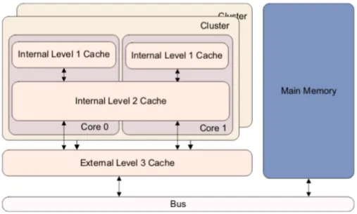
The ARMv8 specification defines three different cache levels; the proces-sor can then implement an arbitrary number of them. The cache levels are distinguished based on their position on the route from the single core to the external memory.
In figure 3.5 we can see the disposition of the levels. The distance from the core issuing a memory access is also an important factor in performance. When a core requires a memory location, the address is first searched for in the level 1 cache, which is core specific and not shared. If nothing is found the lookup continues hierarchically to the level 2 cache, which is shared among cores but internal to the processor. Another miss results in the third cache level, which is eventually external to the processor.
A specialized device, the cache controller, ensures this search/update mechanism works smoothly. Care must be taken to avoid problematic co-herency situations, where the content of caches and main memory differ.
3.5 Multiprocessor 21
Figure 3.5: Position of different cache levels in the system.
Since the objective of this work is to build an educational experience performance is not a relevant factor; therefore, caches are simply disabled altogether. Yet a generic understanding of caching is required to correctly setup memory attributes when configuring the MMU.
3.5
Multiprocessor
Although not mandatory, the ARMv8 architecture is specifically struc-tured to host systems with more than one core, like the Cortex-A53 CPU. In a multicore environment each core has both personal and shared resources: the registers (general purpose and system) are tipically duplicated and have a localized effect, while the main memory is shared by all cores at all times. As seen in the previous section the same applies to caches, with memory banks closer to the core itself being personal while others are shared.
Each core has its own execution thread, identical or different from the others. The A-53 processor has a single clock input, so every core runs at the same frequency.
At a shallow level, the only register one should be concerned with when dealing with parallelism is MPIDR ELn . It contains the identifying num-ber for both cluster and core that is currently executing, so reading it yields different results depending of who is doing it. On the A-53 there is only one
cluster and four cores (indexed from 0 to 3).
When the reset interrupt is fired execution starts only for the first core; the remaning three are held in a waiting state (as if by executing a WFE instruction). They can be woken up by executing a SEV (send event) instruc-tion, at which point execution starts at address 0x80000 for everyone else. The most immediate way to split execution into different threads is to check MPIDR and follow up with a conditional branch. From there each core should be parked in a spinlock, waiting to be released and directed towards the code it should execute.
3.6
ARM Timer
The Cortex A-53 implements a generic ARM timer interface that can be used for interrupts and time scheduling. Despite its apparently simple purpose this is a very convoluted internal device used to virtualize timers for guest OSes as well. Given such functions are not needed in this work, the explaination will focus on the physical counter and interrupt setting registers. First of all, the timer must be initialized. It has a fixed running frequency of 62.5 MHz that increments a 64-bits counter on each tick, but by default the timer registers cannot be accessed at lower exception levels. Setting the proper bits of CNTHCTL EL2 and CNTKCTL EL1 signal clearance of access from EL2 and EL1 to lower levels, respectively.
From there, every exception level (and each core) but EL0 have its own timer to configure and use freely. Additionally, EL1 and EL2 can benefit from a virtual timer with a counter value equal to the physical one minus a specified offset (register CNTVOFF), for a total of five channels. Each timer is controlled through four classes of registers:
• Control: 32-bits registers named CNTt CTL ELn , where t
repre-sents the kind of timer (e.g. P for physical, V for virtual, H for hyper-visor) and n is the exception level. They only use 3 bits to determine whether the timer is enabled, if the interrupt should be masked and if the condition has been met (i.e. the time alarm has been reached).
• Counter: the ever growing 64-bits counter register, named CNTt CT ELn .
• Compare Value: CNTt CVAL ELn , holds the compare value of
the corresponding timer. The condition for the timer is met when Counter − CompareV alue >= 0.
3.6 ARM Timer 23
for setting the next timer interrupt. On write, the compare value is set to the current timer plus the written timer value.
The memory mapped generic interrupt controller can be used to decide which kind of interrupt (IRQ or FIQ, if any) is fired on condition met. Then, an appropriate value can be loaded onto the timer value register, and even-tually an exception will be fired. Timer interrupt lines are de-asserted either by setting a new timer in the future or by disabling the counter altogether. Even at the same exception level, physical and virtual timers have separate interrupt lines. In this project both are used at EL1 by the abstraction layer: the physical line is routed to normal interrupts while the virtual one is managed by a FIQ.
Chapter 4
The Memory Management Unit
The Memory Management Unit is a device found in most CPUs tasked with the objective of translating from virtual memory addressing to physical addressing. The Cortex-A53 is no exception and has an advanced internal MMU. It is such an important component of the system and of any Oper-ating System that even if it’s technically part of the ARMv8 specification it deserves a chapter on its own.
The main purpose of address translation is to allow each process to have its own virtual address space that has nothing to do with how much memory is available (and where this memory is located) on the system, with hardware MMIO and other processes hidden from its view. If the memory management unit is active any address referenced by a process is first elaborated and translated: different sections of the 64-bits address (starting from the most significant) are used to index different levels of a tree containing translation entries. While translating there can also be additional checks on whether the current exception level has the proper permissions to access the resulting physical memory. For example memory blocks where the kernel is loaded should not be accessed in any way by EL0 code; in a similar way memory that is writable at EL0 cannot be allowed to execute at higher permission levels. The latter constriction is built in the specification by default; the former should instead be enforced by the developer via MMU configuration. Only after translation and permission checks are done the actual memory access is performed; however, most of the process is handled by the hardware and can be almost entirely ignored by the programmer after the initial setup.
4.1
Address Translation
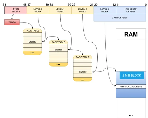
As briefly mentioned in the introduction, when the MMU is active every address is treated as an array of indexes for the translation table. The trans-lation table is a tree of transtrans-lation entries that maps a section of RAM: each level of the tree has entries covering a certain number of elements in the next level until the last, that corresponds directly to memory.
The example that follows considers a tree where each entry before last level points to 512 more entries and depicts a trivial “identity” mapping: every virtual address is translated in the same physical address. The bottom level covers a 4KiB block of memory directly (the reason for these numbers will be explained in section 4.1.1). There are four levels in the tree, level 0 to 3. Presume we want to translate a 64-bits address:
• the 16 most significant bits are reserved for kernel space virtualization
(more on this topic in section 4.4).
• bits 47:39 are the level 0 table and reference a level 1 entry. Each level
0 entry spans a 512 GiB memory range (239).
• bits 38:30 are the level 1 table and reference a level 2 entry. Each level
1 entry spans a 1GiB memory range (230 or 512GiB/512).
• bits 29:21 are the level 2 table and reference a level 3 entry. Each level
2 entry spans 2 MiB memory range, similarly to previous levels.
• bits 20:12 are the level 3 table and reference the last level, made of
direct memory blocks. Each memory block is 4KiB wide.
• bits 12:0 are the offset for the last memory block and index the actual
word referenced.
In this mundane example it is evident how the translation process is arbitrary; every level can simply be cut off and the resulting address be obtained by adding the intermediate indexes and the remaining bits (to be considered as the final offset).
This is not possible anymore if the translation function is not an identity, in which case the translation function is codified by the pointers in the table entries; the table entry marks the beginning of the next level of tables and the corresponding piece of virtual address indexes the chosen entry.
4.1.1
Granule Size
With granule size we refer to the smallest possible block of memory that can be indexed by the MMU tables; in the previous example, 4KiB. The
4.1 Address Translation 27
Figure 4.1: Example of the address translation process .
ARMv8 specification allows for three different granule sizes: 4KiB, 16KiB and 64KiB. The actual ARM processor abiding to the standard can in turn implement those granules only partially, and fortunately the Cortex-A53 im-plements them all. The granule size is a global setting, affecting the entirety of the page table. Different granule size dictate how many levels is possible to have and how many entries are in each table (for example, a granule of 64 KiB allow only 3 levels and a granule of 16KiB will result in 10-bits wide address sections).
A small granule size will result in more control but also in a bigger table; to divide a 2GiB RAM into 4KiB blocks an Operating System will need 524288 64-bits wide table entries, for a total of 4MiB of allocated memory. Choosing a fine grained control does not mean commiting to it, however. If there are large sections of memory with the same memory attributes and virtual addressing (e.g. MMIO memory that should generally not be accessed by user processes) the developer can “cut early” the page table tree and use any intermediate memory range. In the above example we could arbitrarily stop at level 2 and create a part of the table with direct entries spanning 2 MiB each, situation photographed in figure 4.2.
Figure 4.2: Here the last 21 bits are used as a bigger offset for a 2 MiB block of memory
4.2
Table Descriptor Format
When in AArch64 there is a single accepted format for table entries. We will now consider the configuration consequential to a 4 KiB granule size; other choices differ sligtly in translation indexes width and position, but maintain the same core concepts. The table descriptor is 64-bits wide, separated in differently sized fields.
Any table entry is one of two types:
1. A table descriptor that points to another table entry in the next level.
2. A block entry that resolves directly into a memory range of variable size, depending on the level.
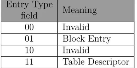
The entry type is defined by the two least significant bits in the descriptor, as depicted in table 4.2; an invalid entry leads to an MMU fault exception.
4.2 Table Descriptor Format 29 Entry Type field Meaning 00 Invalid 01 Block Entry 10 Invalid 11 Table Descriptor
Table 4.1: Page entry types.
Note that not every level can host a block entry; with a granule size of 4 KiB, level 0 does not admit that kind of descriptor.
4.2.1
Table Descriptors
Table descriptors point to a table entry in the next level. Bit fields have the following meaning:
• [0] marks the validity of the entry; 1 is valid, 0 is invalid. • [1] is the entry type. It is 1 for table next level descriptors. • [2:11] are ignored/reserved bits.
• [121:47] is the address of the next level table. It is codified as if it
started from the least significant bit, with [112:0] bits assumed as 0. Because of this all page tables must be 4096 (212) bytes aligned.
• [48:58] are ignored/reserved bits.
• [59] PXNTable field: private execute never bit for subsequent levels of
lookup; if set the memory range covered by this and following entries cannot be executed by code at level EL0.
• [60] XNTable field: execute never bit for subsequent levels of lookup;
if set the memory range covered by this and following entries cannot be executed.
• [61:62] APTable field: access permission bits for subsequent levels of
lookup; this field enforces permission rules for the memory range in-dexed by this and following entries, combined in a hierarchical fashion (see table 4.2.1). Subsequent table entries can further restrict the per-mission rules but cannot loosen them; failure to heed said rules will result in an appropriate abort exception.
1This value can be different for granule sizes other than 4KiB 2see footnote 1
• [63] NSTable field: when in secure state this bit specifies the security
state for subsequent levels of lookup. When not in secure state it is ignored.
APTable[1:0] Restriction
00 No effect on subsequent levels of lookup
01 Any access to this memory range from EL0
is forbidden.
10 Memory is read-only.
11
Any access to this memory range from EL0 is forbidden, while it is read-only for
higher privilege levels.
Table 4.2: Access Permission Table bit fiels. The two bits can be separated and seen as read-only bit ([0]) and EL0 access ([1])
4.2.2
Block Descriptors
Block descriptors represent direct access to a block of memory; when one is reached, it is the last stage of the translation process. They contain the following bit fields:
• [0] marks the validity of the entry; 1 is valid, 0 is invalid. • [1] is the entry type. It is 0 for block descriptors.
• [2:4] memory attributes index field. The value found here indexes a
memory address configuration defined in corresponding the MAIR ELn register (see section 4.3).
• [5] is the non-secure bit. For memory accesses from secure state
spec-ifies whether the output address is in the secure or non-secure address map. For accesses from non-secure state this bit is ignored.
• [6:7] are data access permission bits. Similar to APTable bits, they
are referred to the immediate block of memory (and can be further restricted by previous APTable settings). For possible values see table 4.3.
• [8:9] sets the shareability of the memory block, configuring caching
4.2 Table Descriptor Format 31
AP[2:1] Access from privileged EL Access from EL0
00 Read and write Forbidden
01 Read and write Read and write
10 Read-only Forbidden
11 Read-only Read-only
Table 4.3: Access Permission Bits values. similarly to 4.2.1, the two bits 1 and 0 can be interpreted separately as write restriction for higher exception level and access for EL0, respectively.
• [10] is the access flag (AF). If it is not set it means the selected entry
is accessed for the first time, in which case an MMU abort will be fired. The exception handler should take care of the initialization, set the access flag to 1 and attempt again the memory access.
• [11] is the not global bit (nG ). If a lookup using this descriptor is
cached in a TLB, determines whether the TLB entry applies to all ASID values or only to the current ASID value (see section 4.5 for more).
• [12:47] is the address to the memory block that is pointed by the
descriptor. It is aligned similarly to the address in a table descriptor, but it contains actual memory instead of a next level page table.
• [48:50] are ignored/reserved bits.
• [51] is the Dirty Bit Modifier (DBM); it is used to keep track of
dif-ferences between caches and real memory. If it is set, caches should be checked for stale entries. It can be managed either via hardware or software.
• [52] is the Contigous bit, a hint bit indicating that the translation table
entry is one of a contiguous set or entries and may be be cached in a single TLB entry.
• [53] PXN bit: privileged execute never bit. If set, the memory block’s
execution at unprivileged exception levels (EL0) is forbidden.
• [54] XN bit: execute never bit. If set, the memory block’s execution is
forbidden.
4.3
Memory Types and Attributes
As previously mentioned the block and table descriptors contain infor-mation about what kind of memory they point to. Every memory address is one of two possible types: normal or device. Normal memory is the one used for most memory regions and where there can be the most invasive op-timizations. Normal memory can be heavily cached and is considered to be weakly ordered: the actual number, time and order of access can differ from the logical flow of the program without causing semantic errors.
Device memory is used instead for memory mapped peripherals. When the subject is a device register the order of operations and even repeating the same instruction might yield unexpected side effects; caching must be disabled too, as the content of a device bus is often non deterministic. Other than the memory type there are fine tuned attributes to distinguish what levels of caching and optimization are allowed.
4.3.1
Shareability
In a multiprocessor system the main memory is obviously shared among all the cores. This can lead to coherency problems in caches external to the individual core (level 2 and level 3, see section 3.4). Hinting who is going to use a certain memory block can greatly help the system when managing caches, improving performance and energy cost. There are three possible shareability options:
Non-Shareable: memory marked as non shareable is assumed to belong to a single actor, thus synchronization of access from different cores is not needed.
Inner Shareable: this memory can be shared inside the processor (i.e. be-tween the cores) but not outside of it (i.e. in the rest of the system). Outer Shareable: an outer shareable domain is publicly available for every
actor in the system and needs to be synchronized on each access.
The shareability attribute is found in the specific field of the block entry descriptor (see section 4.2.2)
4.3 Memory Types and Attributes 33
4.3.2
Cache policies
When a cache search misses and the entry is not found, the respective cache entry is updated with the value found on RAM. When the search is successful and the operation is a write, deciding what location to update is not trivial.
Regarding normal memory, the OS developer can specify cache policies as any combination of the following three classes:
1. Cacheability: Non-Cacheable, Inner Cacheable or Outer Cacheable. 2. Update policy: Write Back or Write Through.
3. Transient: Transient or Non-Transient
Different cacheability options refer to which fast memory block should be used - internal to the core, internal to the cluster or external - and were described in section 3.4.
When write back memory locations are updated only the cache entry is mod-ified and marked as dirty; corresponding main memory locations are updated only when the cache line is evicted or explicitly cleaned. Write through is instead a safer (but slower) approach, where an update changes both the cache and the system memory.
Transience is an hint to the cache controller about how long an address should be kept in cache for. This behaviour is implementation defined, not configurable by the developer.
Device memory is treated differently, and thus possesses its own set of attributes:
1. Gathering: this property determines whether multiple accesses can be merged into a single bus transaction for this memory region. If the address is marked as gathering the processor can, for example, merge two byte writes into a single-word half write.
2. Reordering: attribute defining whether accesses to the same device can be re-ordered with respect to each other. If the address is marked as non Re-ordering then accesses within the same block always appear on the bus in the order specified by the code, while Re-ordering ranges of memory will be subject to read and write chains optimization. 3. Early Write Acknowledgement: identified as E or nE, declares if
an intermediate write buffer between the processor and the slave device being accessed is allowed to send an acknowledgement of a write com-pletion. It is only used for closely intertwined operation with special peripherals.
Refer to the Architectural Reference Manual [14] for the exact values and codes of the memory attributes combinations.
4.3.3
MAIR Configuration
Due to the high number of possible combinations (many of which are problably scarcely used), the memory attributes configuration procedure fol-lows a peculiar and somewhat unconventional approach. Instead of having separate fields in the already filled block descriptor format, the programmer defines up to eight memory attribute combinations codified with 8 bits each which are then pushed into the MAIR ELn register as if in an array. The block descriptor in turn has a 3-bits field, the memory attribute index, that indexes which configuration to use in said array, in a two step process.
In the image example, the MAIR register is populated with two options for cached and non-cached normal memory in the first two bytes. Page table entries will then select a combination using the memory attribute index. Note that any combination can be placed anywhere in the register and it does not need to be correctly initialized in all the eight bytes, as long as only correct entries are indexed by the page table.
Figure 4.3: MAIR register configuration and indexing by the page table entries.
4.4 Kernel Space Virtualization 35
4.4
Kernel Space Virtualization
In a tipical OS environment multiple processes run concurrently and use dynamically allocated memory and resources. The memory management unit serves to this purpose: every process has its own set of translation tables managed by the kernel and sees a contiguous range of memory at its disposal while in truth it is loaded somewhere in main memory - maybe not even adjacent or complete.
In this multitude of actors we can consider the kernel as a process in its own right - albeit of a superior kind - and because it has no peers and often uses a static memory space the translation mechanism is meaningless, if not cumbersome.
To fix this situation the ARMv8 provides a number of features. One may intuitively imagine different page table references for each Exception Level, but this is only partially the case. EL0 and EL1, the main levels of operation for user processes and kernel, share in fact the same two page table registers: the one assigned to “normal” operation, TTBR0 EL1, and the register actually in charge to properly divide user and kernel pages, The former is used to translate addresses in the vast majority of the immense 64-bits addressing space, holding the base address of the page table constructed by the developer; TTBR1 EL1, the latter, works in the same way but is only selected when the 16 most significant bits of the address under scrutiny are set to 1, forming a location absurdely far away for any memory bank designed in the foreseeable future.
The kernel can then operate in this mock memory range with a personal page table (possibly as an identity transformation) while normal processes live in lower scope of virtual memory. To accomodate the kernel in this in-existent range the addresses in its code must be set properly. This would require either a linker script instructing to compile for memory starting at 0xFFFF00000000000000 (in which case the MMU must be configured and enabled immediately) or compiling the code for relative branch instructions only. The latter approach is considered easier as it works even if the MMU is disabled and only requires the kernel entry point (the exception table) to be tweaked when address translation is eventually turned on.
As a side note, the condition to select the TTBR1 EL1 register can be limited to the second most significant byte of the address set to 0xFF; the first byte can then be freely used by the kernel software for personal purposes.
An example use case might be in support of object-oriented programming languages: as well as having a pointer to an object, it might be necessary to keep a reference count that keeps track of the number of references, pointers