Università Degli Studi di Catania
Dipartimento Di Fisica e Astronomia
Dottorato di Ricerca in Scienza e Tecnologia dei Materiali
XXVII Ciclo
ANTONELLA GENTILE
Structural and optical properties
of complex-morphology materials
based on
metal nanostructures
Tesi di Dottorato
Tutor: Prof.ssa M. G. Grimaldi
Supervisor: Dott. F. Ruffino
Coordinatore: Prof.ssa M. G. Grimaldi
UNIVERSITÀ di CATANIA
Dipartimento di Fisica e Astronomia
Dottorato di Ricerca in
Scienza e Tecnologia dei Materiali
XXVII CICLO
A. A.
2014/2015
etÜx áÉÇÉ Äx ÑxÜáÉÇx v{x âátÇÉ Ät ÅxÇàxA
cÉv{x vÉÄÉÜÉ v{x âátÇÉ |Ä vâÉÜx x
âÇ|v{x vÉÄÉÜÉ v{x âátÇÉ xÇàÜtÅu|A
3
Dottorato di Ricerca in Scienza e Tecnologia dei Materiali
XXVII Ciclo
ANTONELLA GENTILE
Structural and optical properties of
complex-morphology materials based
on metal nanostructures
Tutor: Prof.ssa M. G. Grimaldi
Supervisor: Dott. F. Ruffino
Coordinatrice: Prof.ssa M. G. Grimaldi
Tesi per il conseguimento del titolo
A.A. 2014/2015
L
IST OF ABBREVIATIONS
Abs: Absorption
AFM: Atomic Force Microscopy
BF: Bright Field
CCA: Cluster-Cluster Aggregation
DDA: Discrete Dipole Approximation
DLA: Diffusion Limited Aggregation
EDX: Energy Dispersive X-Ray
EELS:
Electron Energy-Loss Spectroscopy
EFTM
:Energy Filtered Transmission Electron Microscopy
EF: Enhancement Factor
EM: Electromagnetic
FA: Filled area
FF: Fill Factor
FIB: Focused Ion Beam
FL: Fermi-Level
FDTD: Finite Difference Time Domain
FTIR: Fourier Transform Infrared
FTO: Fluorine Tin Oxide
5
Is: Islands
LTM: Light Trapping Multilayer
MB: Methylene Blue
MIGS’s:
Metal-Induced Gap States
MOM: Metal-Oxide-Metal
MNPs: Metal Nanoparticles
MS: Metal/Semiconductor
NDs: Nanodendrites
NP: Nanoporous
NPs : Nanoparticles
NSOM: Near Scanning Optical Microscopy
NSs: Nanostructures
NWs: Nanowires
PV: Photovoltaic
RBS: Rutherford Back Scattering Spectroscopy
R&G: Recombination and Generation
RRS: Resonant Raman Spectra
SBH: Schottky Barrier Height
S/C: Semiconductor Contacts
SEM: Scanning Electron Microscopy
SLS: Solid Liquid Solid
SOI: Silicon On insulator
SOS: Silicon On Oxide
SPPs: Surface Plasmon Polaritons
SPRs: Surface Plasmon Resonances
SERS: Surface Enhancement Raman Scattering
t_ FTO: Textured Fluorine Tin Oxide
TEM: Transmission Electron Microscopy
VLS: Vapor Liquid Solid
7
Contents
Introduction: general overview and outline
11Chapter 1
Complex-morphology materials based on metal nanostructures
17
1.1 Metal nano-scale size structures with complex shape and composition: synthesis
methods, properties and applications 18
References 35
Appendix : other complex morphologies metal based materials 39
References 52
Chapter 2
Structural and optical properties of branched metallic nanostructures
for SERS applications
54
2.1 Metallic dendritic nanostructures: motivations and state of the art 55
2.1.1 Motivations 55
2.1.2 State of the art: synthesis technique and growth kinetic 56 2.2 Multibranched structures: the physics of the snow crystal 60 2.3 Structural and optical properties of solid-state synthesized Au dendritic structures 63
2.3.1 Introduction 63
2.3.3 Results 64 2.3.3.a General effects of the thermal processes 64
2.3.3.b General effects of the substrate and temperature 71
2.3.4 Optical measurements 73
2.3.5 Phenomenological growth model 75
2.4 Applications: Au dendrites as SERS-active substrates 77
2.5 Conclusions 82
References 83
Chapter 3
SiO
2Nanowires-Au Nanoparticles pea-podded composites: synthesis
and structural analyses
86
3.1 SiO2 nanowires-Au nanoparticles pea-podded composites: motivations and state of
the art 87 3.1.1 Synthesis technique and growth kinetics 89
3.1.1.a Vapor Liquid Solid (VLS) growth mechanism 89 3.1.1.b Solid Liquid Solid (SLS) growth mechanism 92 3.1.2 Rayleight instability 93 3.2 SiO2 Nanowires-Au Nanoparticles pea-podded composites: synthesis and
structural analyses 96 3.2.1 Experimentals 96
9
3.3 Results and discussion 97 3.3 Range of applications 105
3.4 Conclusions 108
References 109
Chapter 4
Nanoscale structuration, structural, optical and electrical properties of thin gold
films on textured FTO substrates for photovoltaic applications
112
4.1 Electronic device for solar energy conversion 113 4.1.1 p-i-n junctions 113 4.1.2 Metal/Semiconductor (Schottky) contacts 114 4.1.3 Electron transport at metal-semiconductor (MS) interface 115 4.1.4 I-V characteristics of the solar cell under dark or light condition 118
4.1.5 How to maximise the solar cell paramrters: VOC, ISC and FF 122
4.2 Plasmonic nanostructures for improving PV devices 124
4.3 Plasmonic solar cells: correlation between the MNSs properties and the devise
Performance 127 4.4 Nano-scale structuration and optical properties of thin gold films on textured FTO
(t-FTO) substrates 131 4.4.1 Experimental details 133 4.4.2 Structural and optical characterizations of the glass/t-FTO substrate 135
4.4.3.a LTM synthesis by furnace thermal annealing 137 4.4.3.b Synthesis and characterizations of the LTM by nanosecond
laser irradiations 139 4.5 Applications: thin film solar cell containing Au nano-particles at the textured
FTO/p-i-n interface (t-FTO/Au NPs solar cells) 147 4.5.1 Fabrication of t-FTO/Au NPs solar cells 147 4.5.2 Electrical properties modulation of the t-FTO/Au NPs solar cells 150
4.6 Conclusions 152
References 155
Summary and conclusion
159List of publications
162Contributions to international conferences
163Participations to international schools
164Acknowledgements
16511
Introduction: general overview and outline
For their peculiar properties, metal nanostructures have been extensively used in applications such as catalysis, electronics, photography and information storage, among others. New applications for metals in areas such as photonics, sensing, imaging and medicine have also being developed. Significantly, most of these applications require the use of metals in the form of nanostructures with specific controlled properties. The properties of nano-scale metals are determined by a set of physical parameters, which include the size, shape, composition and structure.In recent years,many research fields have focused on the synthesis of nano-scale size metallic materials with complex shape and composition in order to optimize the optical and electrical response of devices containing metallic nanostructures. This thesis work is in line with this field of scientific literature.
We begin with an overwiev of the basic concepts on the correlation between structural and optical parameters of nano-scale metallic materials with complex shape and composition, and the possible solutions offered by nanotechnology in a large range of applications (catalysis, electronics, photonics, sensing). The aim is to assess the state of the art and, then, show the innovative contributions that can be proposed in this research field.
Then, we report on innovative, versatile and low-cost synthesis techniques, suitable to provide a good control on the size, surface density, composition and geometry of the metallic nanostructures. The main purpose of this study is the fabrication of functional nanoscale-size materials, whose properties can be tailored (in a wide range) simply by controlling the structural characteristics. The modulation of the structural parameters is required to tune the plasmonic properties of the nanostructures for applications such as biosensors, opto-electronics or photovoltaic devices and SERS-active substrates.
The structural characterization of the nano-scale materials is employed in order to define how the synthesis parameters affect the structural characteristics of the resulting metallic nanostructures. Besides, macroscopic measurements are used to probe their electrical and optical properties. Phenomenological growth models are drafted to explain the processes involved in the growth and evolution of such composite systems. After the synthesis and characterization of the metallic nanostructures, we study the effects of the incorporation of the complex morphologies on the optical and electrical responses of each specific device.
The structure of the present work is as follows:
- Chapter 1 “Complex-morphology materials based on metal nanostructures”: in this Chapter, we explain the motivations to synthesize metal nanostructures with complex geometry and composition. The need to create morphology alternatives to isotropic shapes, such as spherical geometry, comes from the strong correlation between the structural characteristics and the response of the Localized Surface Plasmon Resonances (LSPR) of the nano-structured metallic materials. The flexibility and scope of the change are highly sensitive to the specific structural parameter. For this reason, we report some experimental studies that demonstrate that the shape and structure of an Au or Ag nanocrystal play the most important
role in determining the number, position and intensity of LSPR modes. Such works show that the LSPR of a single metallic nanoparticle can be shifted in frequency via alterations in particle shape and size. Besides, in nanoparticle ensembles, additional shifts are expected to occur due to the electromagnetic interactions between the localized modes related to neighboring metal nanoparticles. Both experimental and computational studies highlight that two regimes have to be distinguished, depending on the magnitude of the interparticle distance. For closely spaced particles, near-field interactions dominate, and the particle array can be described as an array of point dipoles interacting via their near field. Therefore, interparticle junctions serve as hot-spots for field enhancement, which will be further discussed in Chapter 2 in a context of Surface Enhanced Raman Scattering (SERS). Therefore, the interparticle coupling will lead to shifts in the spectral position of the plasmon resonance compared to the case of an isolated particle. On the contrary, for larger particle separations, far-field dipolar coupling dominates. Far-field coupling field has pronounced influences on the plasmon lineshape, both in terms of resonance frequency, as well as spectral width. Taking into account these properties of plasmonic nanostructures, we report the more common synthesis methods and experimental results related to metal nanostructures with complex shape and composition Taking into account these properties of plasmonic nanostructures, we report the more common synthesis methods and experimental results related to metal nanostructures with complex shape and composition (e.g. metallic dendritic nanostructures, SiO2 nanowires-Au nanoparticles pea-podded) for advanced applications in
the field of electronics, opto-electronics, sensing, bio-sensing and for magnetic devices. In the Appendix to this Chapter, we report the correlation between structural and optical parameters related to other complex morphologies metal based materials (e.g. gold nanoring and ring dimmers, gold nanorice, nanoporous gold films, nanoporous Au NWs, etc.)
- Chapter 2 “Structural and optical properties of branched metallic nanostructures for
SERS applications”: this Chapter reports the motivations that lead to synthesize branched metallic nanostructures and the state of the art.
Metallic nanodendrites, defined as large fractal aggregates, with hyperbranched architectures have attracted much attention due to their importance in understanding the fractal growth phenomena (to be distinguished from non-fractal structures such as compact or periodic geometries), and their potential applications in functional devices, plasmonics, biosensing and catalysis. To explain the synthesis techniques and growth kinetics, we report many experimental works. In these works, the controlled growth of Au dendritic structures is obtained using chemical synthesis methods. The analyses of the experimental results suggest that the growth conditions strongly affect the morphology of the resulting complex nanostructures. Indeed, the interaction between chemical solutions and growing metal crystals results in a delicate balance between the diffusion and reaction rate under non-equilibrium conditions, favoring the formation of planar dendrites with a symmetric single-crystalline structure. The well-known growth mechanisms
13
under non-equilibrium conditions are explained on the basis of the Diffusion Limited Aggregation (DLA) model and Cluster–Cluster Aggregation (CCA) model. In a DLA regime, the growth takes place by bonding of individual atoms to the growing surface after the reduction of the metal ions. Whereas, according to the CCA model, the individual metal clusters aggregate to form a branched morphology. Besides, to understand the processes involved in the transiction from faceting to branching, we report the physics of a snow crystal. When the crystal growth is dominated by attachment kinetics, the resulting crystals are faceted. Instead, when the particle diffusion dominates the crystal growth dynamics, branching occurs. If the crystal morphology exhibits numerous branches and side-branches, then the growth is dendritic, which literally means “tree-like”. Dendritic crystal growth is one example of the more general phenomenon of pattern formation in non-equilibrium growing systems.
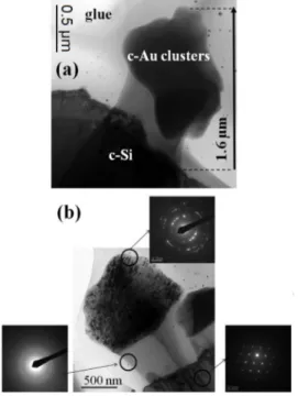
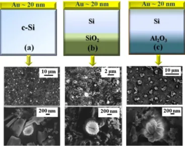
In comparison with the methods reported in the literature, we also suggest a simple and versatile physical procedure for obtaining Au dendrites (Au Ds), reminiscent of fractal structures, on sample surfaces. In particular, we observe a peculiar structural evolution of the Au film (20 nm thick film) on Si substrate from a continuous coating to Au Ds as a consequence of thermal treatment at 1373 K (1100 °C), in the presence of fast heating and cooling stages (1373 K/min.). Our structural characterizations of Au dendrites suggest that these structures are formed by Si atoms originating from the substrate and are covered by crystalline Au nanostructures. In order to understand the formation mechanism of the dendritic structures, the role of the substrate (using three different substrates: c-Si, poly-Si and SOS) and the temperature (the samples have been processed at three different temperatures, T1 = 1073 K, T2 = 1273 K and T3 = 1373 K) in
the growth process are investigated.
Besides, we draft the phenomenological model for the growth of the dendritic structures by considering the kinetic processes that occur at the Au-Si interface in a far-from-equilibrium condition.
Finally, we report the results of the optical measurements that show the efficient behavior of the Au Ds as scattering centers in the infrared region of the spectral range. In addition, SERS measurements, performed by MB or thiophenol as probe molecules, highlight that dendritic nanostructures can be used as SERS-active substrate to obtain amplification factors of electromagnetic field, due to the resonant coupling between the Raman signal and plasmonic oscillations related to sharp metallic tips of the Au dendritic structures. The comparison between SERS spectra related to Au Ds on different substates suggests that to obtain higher EF, the planar size of the Au dendrites, and then, the SERS-active area, must be in µm-scale. Also, the dendrite surface must be uniformly covered by Au, such that most MB molecules are adsorbed to the dendritic structures.
Another important result, from SERS measurements, is the depolarization factor of the silicon
signal due to the interaction between laser radiation and dendritic structures. The changes of the characteristic ratio between the polarized components of the Si signal
- Chapter 3 “SiO2 Nanowires-Au Nanoparticles pea-podded composites: synthesis and
structural analyses”: in this Chapter, we explain why the research in biosensing and optoelectronic devices is focused on the study of the structural and optical properties of metallic nanoparticles (MNPs) embedded in the dielectric matrix. Many works in the literature have shown that noble metal nanoparticle-dielectric matrix composite systems have practical applications in ultrafast all-optical switching devices owing to their enhanced third-order nonlinear susceptibility, especially near the surface-plasmon-resonance (SPR) frequency. Therefore, metal-dielectric nanocomposites (see SiO2
nanowires-Au nanoparticles pea-podded composites) have been applied in optical switching devices for non-linear and fast optical response near the SPR. The experimental results in the literature have suggested that the electronic, optical and magnetic properties of metal NPs embedded in a dielectric matrix depend on the size and shape of NPs, the interparticles distance and the dielectric costant of the surrounding medium. To understand the growth dynamics of these composite systems, we report the most common synthesis approaches, such as the sol-gel process, metal-dielectric co-sputtering deposition, metal-ion implantation into a dielectric matrix and pulsed laser deposition, to prepare metal-dielectric nanocomposites. Taking into account the previous literature, we focus our attention on a simple and versatile method for the direct growth of SiO2 NWs on Si surface (a method allowing direct applications in Si-based
solid state devices). We observe that amorphous SiO2 NWs can be grown on a crystalline Si
substrate by first deposting a thin metal film (Au, for example) on its surface, and then heating the system to elevated temperature (>1273 K), in an inert ambient (e.g. N2 or Ar), containing
trace amounts (3–5 ppm) of oxygen. Typical annealing conditions for the growth of such a structure are 60 minutes at 1373 K (1100 °C). The prevalence of such bead strings in the SiO2
nanowires depends critically on the growth conditions and may vary between about 1% and 80%, even on a single wafer. In particular, after the growth of SiO2 nanowires-Au nanoparticles
pea-podded composites (from 30 to 150 nm in diameters and until 1mm in length), using TEM analyses, we proceed to the quantification of the SiO2 NWs diameters (DNWs) and Au NPs
diameters (dNPs) embedded in them, in order to establish a specific correlation between DNWs
and dNPs. A further correlation is established between the diameter of the Au NPs embedded in a
single NW and their center-to-center distance (sNPs). From the experimental correlations of such
parameters, information on the characteristics of the mechanisms governing the formation of the SiO2 NWs-Au NPs pea-podded structures is inferred.
Then, on the basis of the experimental data, we propose a phenomenological model for the formation and time evolution of the SiO2 NWs/Au NPs pea-podded structures, based on the
coexistence of instability and diffusion processes.
- Chapter 4 “Nanoscale structuration and optical properties of thin gold films on textured
FTO”: in this Chapter, we show that thermal treatments of thin Au films, deposited on a glass/textured_FTO (t_FTO) substrate, can induce the growth of Au nanoparticles (NPs), whose
15
structural characteristics can be modulated by varying the parameters of the heating stages. For standard thermal processes, the temperature and time of the heating process are key parameters to induce the gold film break up and NPs growth. The structural characterizations of the thermal treated samples show that a temperature well below the gold melting point (1064 °C) induces the formation of arrays of Au nanodroplets due to the solid-state dewetting process. In particular, the treatment at high temperature (500 °C-180 min) allows a whole break-up of the Au film into nanoparticles, while it induces structural changes of the substrate, so that the electrical response of the glass/t_FTO/Au NPs multilayer is worsened. Our results imply that the standard thermal process at temperature above 400°C does not allow to obtain a glass/t-FTO/Au NPs multilayer with electrical properties suitable for photovoltaic applications.
We also show that laser irradiation at increasing fluence (0.50-1.0 J/cm2) of the samples as deposited optimizes the synthesis process of Au NPs, and preserves the structural and electrical properties of the t_FTO/glass substrates. Electrical measurements, indeed, suggest that the laser operating at 532 nm does not produce any thermal damage due to local heating of the t_FTO layer. Structural analyses of the Au coated-substrates indicate that the metallic films are molten and broken up into discrete-nanometer scale islands after laser exposure. At lower energy, the break up into discrete droplets is incomplete. At fluencies higher than the threshold for break up (1.0 J/cm2), the films are fully dewetted in Au NPs. The comparison between the absorption spectra, related to the substrates covered by 5 nm or 10 nm of Au and submitted to laser treatment at higher energy, indicates an improvement of the absorbed radiation from the sample with larger Au NPs. The simulated trends of the ratio between scattering cross section and absorption cross section in the visible spectral range suggest that the efficiency of absorption dominates over scattering efficiency in the spectral range between 200 and 600 nm for both samples. For wavelength values above 600 nm, instead, the results of the simulation suggest that the glass/t_FTO/Au NPs with larger gold nanoparticles exhibit a reduction of the parasitic absorption and an improvement of the scattering cross section. By varying the NPs radius from about 18 nm to 24 nm, the simulation shows that the scattering remains symmetric in forward and reverse directions. Thus, the experimental results confirm that the surface coverage size distribution of Au NPs is the key parameter to correlate the structural and optical properties of the glass/t_FTO/Au NPs multilayer.
For its peculiar optical and electrical properties, we have introduced the glass/t_FTO/Au NPs multilayer (obtained by nanosecond laser irradiation) with optimized Au NPs coverage size distribution as Light-Trapping-Multilayer (LTM), into thin film solar cells. In order to obtain information about the effects of the introduction of Au NPs at the t_FTO/p-i-n interface of solar devices, the I-V characteristics have been taken into account. The analysis of I-V characteristics under dark conditions indicate a decrease of the Schottky barrier (φB) by increasing the Au NPs
size. This phenomenon induces an improvement of the saturation current (Is) of about one order
saturation current and the reduction of Schottky barrier height (determined by mechanisms such as the recombination or diffusion currents) induce an open circuit voltage (VOC)
reduction, which increases with the improvement of the NPs size. The VOC reduction suggests a higher amount of
recombination phenomena in the solar devices with larger Au NPs at the t_FTO/p-i-n interface, with respect to the reference device. We deduce that the improvement of the recombination processes may be due to the presence of metal-induced gap states or defect-realeted states, in agreement with the FL pinning by electronic states at the MS interface. These processes reduce the light trapping and then the short-circuit current (ISC)values. Indeed, the
analyses of I-V characteristics under light conditions highlight a decrease of ISC due to the
improvement of the parasitic absorption by larger NPs. Thus, we conclude that the incorporation of Au NPs at the FTO/p interface (in the p-i-n structure) induces changes of ISC
and VOC that worsen the solar cell parameters, such as the Fill Factor (FF) and yield factor (η),
17
Chapter 1
Complex-morphology materials based
on metal nanostructures
1.1 Metal nano-scale size
structures with complex shape and composition:
synthesis methods, properties and applications
Nano-scale size materials are materials with at least one dimension between 1 and 100 nm [1]. The crystalline nanomaterials are also characterized by a single-domain crystalline lattice, without the complicating presence of grain boundaries [2]. Scientific interest in nanomaterials has been growing steadily due to their unique position as a bridge between atoms and bulk solids, as well as their fascinating properties and potential applications [3]. The ability to generate such nano-scale size materials is central to advances in many areas of modern science and technology. In principle, the electron confinement by a nano-material provides the most powerful means to manipulate the electronic, optical and magnetic properties of a solid material. This notion explains why nanomaterials have been the primary source for discovering and studying quantum size effects, with examples of quantized excitation [4-7], Coulomb blockade [8], metal-insulator transition [9, 10], and superparamagnetism [11]. Metallic materials have been one of the most ancient fields of study. Among all kinds of inorganic solids, metals deserve special attention because they represent more than two thirds of the elements in the periodic table. Most metals crystallize in the same cubic close-packed (ccp) structure, a face-centered cubic (fcc) lattice that allows for easy characterization. Properties such as strength, toughness, thermal and electrical conductivities, ductility and high melting point make the metals useful for applications ranging from household items to space ship. Traditional applications are mainly based on the bulk metallic properties. New applications exploit the novel properties of metal nanomaterials [12]. Nanomaterials exhibit fascinating size-, shape- and crystal form-dependent properties. Like the bulk metalssize-, nanomaterials of metals are also going to bring profound changes in many spheres of science, technology and industry. Though metal nanoparticles have a long history of preparation and applications, the field has undergone explosive growth in recent years. Metal nanoparticles with excess of morphologies have been prepared, such as polyhedrons, plates, prisms, rods, wires, nanoboxes, nanocages, dumbbells, nanoshuttles, stars, branched rods and wires, dendrites, nanorings, nanotubes, and so on. Such metal nanostructures possess a range of great properties, and many metals have found extensive use in applications that include catalysis [13], electronics [14], photography [15], and information storage [16], among others [17]. New applications for metals in areas such as photonics [8, 19], sensing [20], imaging [21], and medicine [22] are also being developed. Significantly, most of these applications require the use of metals in a finely divided state, preferably in the form of nanocrystals with precisely controlled properties. The properties of a metal nano-crystal are determined by a set of physical parameters that may include its size, shape, composition and structure. In principle, one can tailor and fine-tune the properties of a metal nanocrystal by controlling any one of these parameters, but the flexibility and scope of change are highly sensitive to the specific parameter. For example, in the case of Localized Surface Plasmon Resonance (LSPR) and Surface-Enhanced Raman Scattering (SERS), both computational and experimental studies have demonstrated that the shape and structure of a Au or Ag nanocrystal play the most important role in determining the number, position and
19
intensity of LSPR modes, as well as the spectral region or polarization dependence for effective molecular detection via SERS [23]. In the case of catalysis, it is well-established that the activity of a metal nanocrystal can be enhanced by reducing its size [24]. The selectivity, however, is most sensitive to the packing of atoms on the surface or the exposed facets of a nanocrystal [25]. For example, Pt can selectively catalyze different types of chemical reactions, with the {100} and {210} facets being most active for reactions involving H2 and CO,
respectively [26]. Of course, the facets exposed on a nanocrystal have a strong correlation with the shape. These and many other examples clearly illustrate the importance of shape control to the efficient utilization of metal nanocrystals. The last decade has evidenced the successful synthesis of metal nanocrystals in a variety of shapes. Examples include: sphere; spheroid; cube; cuboctahedron; octahedron; tetrahedron; right bipyramid; decahedron; icosahedron; thin plate with a triangular, hexagonal, or circular profile; and rod or wire with a circular, square, rectangular, pentagonal, or octagonal cross sections. The emergence of many novel approaches induces to synthesis and synthetic design, control of composition, size, morphology, and assembly structure and impressive advances in the characterization and manipulation techniques of metallic nanoparticles. A number of applications have been realized and multitudes of new applications have been envisaged. Among the many morphologies investigated, the anosotropic metal nanostructures have attracted great attention in the last decade due to their unique properties originated in their shape and their potential impact in new technologies. Examples of anisotropic NPs include rods, bars, triangular plates, disks, hierarchical structures among others (fig. 1.1) [27-34].
Figure 1.1 - Examples of silver NPs with different shapes obtained by colloidal synthesis.
(a) Triangular (and some hexagonal) nanoplates. (b) Hexagonal plates. (c) Disklike plates. (d) Tetrahedral NPs. (e) Bipyramids. (f) Cubic and (g) octahedral NPs [34].
By controlling the shape of the particle, the crystallographic planes that are exposed at the surfaces are tailored and, as a consequence, the atomic arrangement that makes the interface with the medium can be tuned. This has been shown to be critical for most chemical-physical properties, expanding the already broad range of applications of NPs. One of the most appealing examples impacted by the shape-dependent properties of NPs is heterogeneous catalysis [35]. Several catalysts are composed by metal NPs dispersed on high surface area supports. In a heterogeneous catalytic reaction, the binding of the reagent molecules and the formation of the new bonds, which will form the product molecules, depend not only on the available orbitals of the reagents but also on the geometry of the atomic arrangement at metal surface. Hence, controlling the exposed facets of a NP can be a major step toward a deeper understanding of the catalytic reaction and the design of better catalysts.
Metals, such as gold and silver, show a resonance in the ultraviolet-visible region of the spectra known as surface plasmon [36]. This resonance arises from collective oscillations of the conduction electrons of the metal and strongly depends on the size, shape, local environment [37], and assembly of the NPs [38]. When a molecule is attached to the surface of a metal NP, its Raman scattering cross section can be enhanced by several orders of magnitude, from 106 up to 109 if the incident light is tuned to the surface plasmon resonance of the particle [39]. This effect, known as SERS, results from an intense local amplification of the electric field near a metal surface when surface plasmon resonates in phase with the incident light. Because the electromagnetic near-field intensity is higher at sharp edges and tips, anisotropic NPs exhibit high Raman scattering enhancement factors that have been exploited for the detection of diluted molecules in analytical applications. For example, Mulvihill et al. [40] explored Langmuir- Blodgett monolayers of cubic, cuboctahedral, and octahedral silver NPs to detect trace amounts of arsenic in water. The best results were obtained with octahedral silver NPs, for which a detection level in the ppb range was achieved.
To understand the effects of the complex shape of the metallic nanoparticles on the plasmonic properties, the results of the optical characterizations related to non-regular geometries are reported. For example, dark-field optical microscopy and near-field optical extinction microscopy enable the observation of plasmon resonances of a single particle. In dark-field optical microscopy, only the light scattered by the structure under study is collected in the detection path, while the directly transmitted light is blocked using a darkfield condenser. This enables the study of single particles dilutely dispersed on a substrate. Figure 1.2 (a) shows as an example of the dipolar plasmon lineshapes related to colloidal silver particles of different shapes. In near-field optical spectroscopy, instead, a thin (metalized or uncoated) fiber tip with an aperture on the order of 100 nm is brought into close proximity of the particle using an appropriate feedback scheme. The plasmon resonances can then be mapped out using either illumination through the tip and collection in the far-field, or evanescent illumination from the
substrate side and light collection via the tip. Figure 1.2 shows scattered light images (fig. 1.2 (b)) and plasmon lineshapes (solid lines in fig. 1.2 (c)) of a variety of gold
21
Figure 1.2 highlights that the localized plasmon resonance of a single metallic nanoparticle can be shifted in frequency from the Fröhlich frequency [41] via alterations in particle shape and size. Besides, in particle ensembles, additional shifts are expected to occur due to electromagnetic interactions between the localized modes. For small particles, these interactions are essentially of a dipolar nature, and the particle ensemble can in a first approximation be treated as an ensemble of interacting dipoles. Two regimes have to be distinguished, depending on the magnitude of the interparticle distance (d).
Figure 1.2 - (a) Scattering spectra of single silver nanoparticles of different shapes obtained in
dark-field configuration. Optical dark field images together with SEM images of individual gold nanoparticles (b) and corresponding scattering spectra (c) for an incident light polarization along the long particle axis [41].
For closely spaced particles, d<<λ, near-field interactions with a distance dependence of d−3 dominate, and the particle array can be described as an array of point dipoles interacting via their near-field. In this case, strong field localization in nano-sized gaps between adjacent particles has been observed for regular one-dimensional particle chains [42]. The field localization is due to a suppression of scattering into the far-field via excitation of plasmon modes in particles along the chain axis, mediated by near-field coupling. Figure 1.3 illustrates this fact by showing the simulated distribution of the electric field above single gold nanoparticles (fig. 1.3 (a)) and a particle chain (fig. 1.3 (b)). From the images, it can clearly be seen that scattering is drastically suppressed for closely spaced particles, and that the fields are instead highly localized at interstitial sites. Interparticle junctions such as these therefore serve as hot-spots for field enhancement, which will be further discussed in Chapter 2 in a context of SERS. Therefore, the interparticle coupling will lead to shifts in the spectral position of the plasmon resonance compared to the case of an isolated particle.
Figure 1.3 - Simulated intensity distribution of the optical near-field above an ensemble of
well-separated gold particles (a) and a chain of closelyspaced gold nanoparticles (b). While for separated particles interference effects of the scattered fields are visible, in the particle chain the fields are closely confined in gaps between adjacent particles. Plasmon resonances were excited using prism coupling with the direction of the in-plane moment component as outlined in the pictures [41].
Maier et al. [43], using one-dimensional arrays of 50 nm gold particles with varying
interparticle distance, demonstrated experimentally the shifts in resonance energy using far-field extinction spectroscopy Due to the strong scaling of the interaction strength with d−3
particle separations in excess of 150 nm are sufficient to recover the behavior of essentially isolated particles.
For larger particle separations, d>>λ, far-field dipolar coupling with a distance dependence of
d−1 dominates. For the example of two-dimensional gratings of gold nanoparticles with various lattice constants, fig. 1.4 shows that far-field coupling has pronounced influences on the plasmon lineshape, both in terms of resonance frequency as well as spectral width. We note that interactions between metal nanoparticles can be further enhanced by providing additional
23
coupling pathways, for example in the form of propagating SPPs for particle arrays fabricated on a conductive substrate [41].
In this subsection, we report the synthesis methods and experimental results of the characterizations related to metal nanostructures with complex shape and composition for advanced applications in the field of electronic, opto-electronic, sensing, bio-sensing and magnetic devices.
Figure 1.4 - Extinction spectra for square two-dimensional gratings of gold nanoparticles
(height 14 nm, diameter 150 nm) with grating constant d situated on a glass substrate [41].
1. Metallic nanodendrites: the field enhancement surrounding nanoscale metallic particles offers an efficient tool to manipulate the light-matter interactions at optical frequencies [44, 45]. For spectroscopic applications, the field confinement near these structures reduces the mismatch between the wavelength of incident light and the size of molecules under study. In the SERS, this propertie can boost the Raman cross section of molecules by many orders of magnitude. SERS offers a very sensitive tool for biological and chemical sensing [46], enabling vibrational spectra to be obtained even from single molecules [47]. The signal enhancement in SERS mostly comes from the excitation of localized surface plasmon resonances (LSPRs) and the “lightning-rod” effect [48]. The latter is particularly pronounced for sharp tips and nanoparticle dimers with small inter-gap size. The optimum substrate for SERS should have the highest average field enhancement possible, be highly tunable, and offer a broad resonance bandwidth, although satisfying all these criteria is very challenging. One of the candidates for a highly tunable substrate is the non-isotropic geometry, such as the dendritic nanostructures. Metallic nanodendrites, defined as large fractal aggregates, with hyperbranched architectures (see fig. 1.5) have attracted much attention due to their importance in understanding the fractal growth
phenomena (to be distinguished from non-fractal structures such as compact or periodic geometries), and their potential applications in functional devices, plasmonics, biosensing and catalysis.
Figure 1.5 - Dendritic structures obtained by electrochemical deposition of copper.
(a) from 0.5M CuSO4/0.5M H2SO4 at 350 mV (frame width = 2.5 mm); and (b) from
0.5M CuClq/0.5M H2SO4 at 500 mV (frame width = 0.6 mm) [49].
Fractal nanostructures can be formed by metals (Au [50, 51], Pt [53, 54], Pd [55, 56], Rh [57, 58], Ni [59], Ru [60, 61], metal oxides [62–65], and semiconductors [66–72]. Because of their higher structural complexity, compared to nanospheres, nanowires and nanodiscs, these
branched nanostructures are expected to have a wide range of technological applications [68, 73]. For example, they have interesting catalytic [60, 61], magnetic [57, 59, 72], optical
[50, 68, 72], and electronic [68, 69] properties, and semiconductor heterostructures have potential uses in solar cells [69]. Branched nanostructures have also been suggested as interconnections in the bottom-up self assembly of future nanocircuits and nanodevices. Therefore, it is important the mechanism by which these structures are formed [52, 70, 72], which is a crucial step toward realizing synthetic control over their structural and functional properties. Synthetic control over the size and shape of these nanostructures is achieved using
25
different chemical approaches. The controlled synthesis of these metal complex morphologies allows the modulation of the optical properties for each specific application.
Au and Ag nanoparticles show a characteristic absorption in the visible region of the electromagnetic spectrum due to the surface plasmon resonance. The position and width of the surface plasmon resonance band are considerably influenced by the size and shape of the nanocrystals. The wavelength dependence of the extinction coefficient is fairly well described by Mie theory [43] for metal particles with sizes much smaller than the wavelength of light [63]. According to Mie theory, the extinction coefficient is given by [74]
[
]
2 2 2 m 1 2 3/2 mε
2ε
ε
ε
λ
Vε
N
18π
k
+
+
=
where λ is the wavelength of incident light, and ε1 and ε2 are the real and imaginary parts of the
complex dielectric function of the metal, and εmis the dielectric constant of the surrounding
medium assumed to be an invariant with respect to the frequency of the light. The overall dielectric constant is given by
2
1
ε
ε
ε
=
+
i
One can readily see that the dependence of the extinction coefficient on wavelength is Lorentzian. Besides, it is known that anisotropic metallic nanoparticles normally exhibit two principal SPR absorption peaks, characteristic of the short (transverse band) and long (longitudinal band) axes.
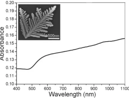
To obtain more information about the changes in the optical response that occurs from a regular to a complex morphology of metallic nanostructures, we report the results of some experimental works. T. Huang et al. [74] show the UV-vis absorption spectrum of the as-prepared Au nanodendrites suspended in water (see inset in fig. 1.6). The spectrum displays a gradual increase in absorption from ~500 nm to the near-IR region without indication of leveling off, which could be attributed to the longitudinal plasmon band, indicating a remarkable overlapping between the transverse band and the longitudinal band. It is well-known that the position and intensity of the longitudinal band depend largely on the size, aspect ratio and mutual coupling of Au nanocrystals. The authors suggest that the observed overlapping between the transverse band and the longitudinal band for the obtained Au nanodendrites could be attributed to the polydispersity in the length and diameter of the trunks and branches, which may lead to a variety of sizes and aspect ratios. The multiple coupling between neighboring trunks and side branches may also result in a longitudinal plasmon band with the position lying in a wide range of wavelengths. So, the observed absorption spectrum may represent a contour combining the size, aspect ratio and coupling factors of the hierarchical dendritic structures.
(1.1)
Figure 1.6 - UV-vis absorption spectrum of Au nanodendrites. The inset shows the Au
nanodendrites grown in mixed DTAB/β-CDsolution. [DTAB]=5.0 mM; [β-CD]/[DTAB]=0.5 [74].
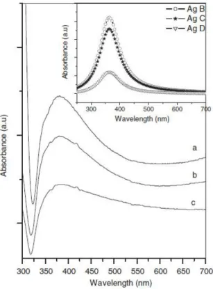
S. Kaniyankandy et al. [75], instead, report the optical properties of silver nanodendrites, synthesized by electrodeposition using AgNO3 as the source in ammoniacal solution. They
reports that SEM patterns of the samples show that as consequence of the addition to the starting solution of a small amount of Ammonia, the deposits (Ag B) show a dramatic change in morphology from irregularly shaped to long strands or rods. Furthermore increase of NH3
(Ag D) is not greatly affect the morphology. The structutal characterizations, shown in this work, indicate that the average value of thickness of the central stem of a dendrite is ~50 nm. Along the central stem (with an average length of ~5 µm), branching is visible for every ~50 nm, and in some cases it is also hyperbranched. The branches of the dendrites are predominantly planar and hyperbranched. To illustrate the changes of the optical properties due to the different morphology of the resulting nanostructures, the authors compare the results of the simulation with the results of the optical measurements (fig. 1.7). The simulation of the UV–vis spectra related to the metal colloids is shown in the inset of fig. 1.7. The authors highlight that the spectra show the Lorentzian nature of the band, and that the decrease in the size of nanoparticles leads to a decrease in the peak height and an increase in the peak width. The experimental UV–vis spectra (fig. 1.7) clearly give a single broad peak with maxima at λ = 380 nm. This indicates that the particles are predominantly spherical and do not have shape anisotropy. Besides, the peak is highly asymmetric and has a large tail towards the lower energy region, i.e. towards red. The peak extends to the entire visible region of the electromagnetic spectrum. This is contrary to the expected Lorentzian line shape. S. Kaniyankandy et al. explain
27
that this result is due to the fact that, according to Mie theory, metal nanoparticles are assumed to be non-interacting spheres. However, in their work the metal nanoparticles are assembled in the form of a supramolecular dendritic structure. Therefore, a considerable amount of interaction is expected among the nanoparticles. Hence, the contribution from higher order multipoles and the distribution of depolarization factors have to be taken into consideration while simulating the absorption spectra. The distribution of depolarization factors in interacting metal spheres gives rise to a shape asymmetry for the SPR band. This has been previously observed by several authors [76]. The peak position at 380 nm is indicative of the particle sizes in the range 20–30 nm. Besides, with increase in the NH3 (hyperbranched nanostructures)
content, the peak position shows only a extremely small shift towards the blue region, indicating a small decrease in the particle size, while the peak width increases with increasing ammonia content in the electrolyte. To explain these effects, the authors consider the size effects of metal nanoparticles. Depending on the size, there exist two regimes in the influence of particle size on the UV–vis spectrum [77].
Figure 1.7 - UV–vis absorption spectra of the samples: (a) Ag B, 0.3M aqueous NH3 solution;
(b) Ag C, 0.6 M aqueous NH3 solution and (c) Ag D, 1.2 M aqueous NH3 solution. The inset
The size regime is defined by the electron mean free path of the metal. For the bulk silver, the electron mean free path is ~52 nm. For particles smaller than the mean free path of the electrons, the influence of the grain boundary scattering cannot be ruled out, and must be taken into consideration. In the scenario when silver particle size is >52 nm, the peak position shows a red shift with increasing size, and the peak width increases with respect to the size (this is defined as an extrinsic size effect). For particle sizes lower than 52 nm, the peak position shows
a very little change towards blue, and the peak width increases with decreasing size. S. Kaniyankandy et al. [75] indicate that this is the intrinsic size effect. In this case, the size of
all samples are in the range where the intrinsic size effect is operational. Therefore, the observation of the increase in the peak width with decreasing particle size can be explained on the basis of the intrinsic size effect. It is interesting to note that the SPR band spreads throughout the entire visible region of the electromagnetic spectrum. This observation is suggestive of aggregated silver nanoparticles, as well as in the present case where the aggregates form an ordered supramolecular structure. This hints at the applicability of these structures in SERS studies, because of an enhancement based on an electromagnetic mechanism, in which the high overlap of incident and scattered light with a metal SPR absorption band is important. The greater the overlap, the higher the enhancement. In the present case, since the SPR band extends throughout the entire visible region, the light of any wavelength in the visible region will be enhanced, thereby giving more flexibility with respect to the application in SERS. Furthermore, the highly branched dendritic structure has a higher surface area, which enables an increase in the sensitivity of SERS [78].
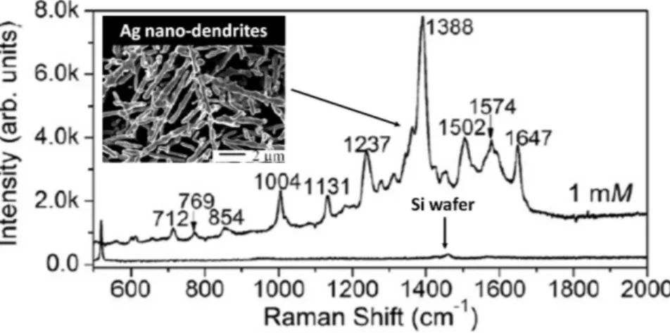
To highlight the good response of the metallic nanodendrites as SERS-active substrates, we report the results of Teng Qiu et al. [79]. They use SERS, which operates with enhanced Raman signals excited by surface plasmons, to investigate C60 nanoclusters. SERS is supposed to
consist of a five-step process: (1) An ingoing photon interacts with the substrate exciting a Plasmon; (2) The plasmon polarizes a molecule bound to the surface, creating a large effective dipole moment; (3) If the molecule now changes the vibrational state, then its molecular polarization alters; (4) The change in molecular polarization couples back into an emitted Plasmon; (5) Finally, the plasmon couples into an outgoing Raman scattered photon. When the C60 nanoclusters are adsorbed on silver nano-dendrites, the symmetry of the C60 molecule is
reduced, resulting in the splitting of the Raman bands from the degenerate modes of C60. As a
result, the number of the vibration modes is greatly increased in the SERS spectrum (fig. 1.8). Besides, the authors couple C60 nanoclusters on the silicon wafer, using a 1mM C60 solution for
comparison. No visible C60 Raman bands (see bottom of fig. 1.8) are observed. The results
suggest that such strong enhancement for the dendritic pattern should be attributed to the fact that the nano-dendrites are assembled on the Si substrate with a very high density and with many horns and, thus, C60 nanoclusters in abundant hot spots between closely spaced dendrite
arms lead to intense SERS enhancement.
Anisotropic nano-objects such as nanorods and nanowires have been shown to possess interesting size- and shape-dependent properties, thus motivating interest in the controlled assembly of them into functional architectures for SERS. Nikoobakht and El-Sayed discovered
29
that SERS intensities are far higher for molecules on aggregated gold nanorod deposits compared with monomeric nanorods, an observation attributed to an enhanced EM field in the inter-nanorod region. In a comprehensive study of Teng Qiu et al., highly ordered and regular silver nanowires with tunable inter-nanowire gap size have been fabricated for placing analyte molecules in hot spots between closely spaced nanowires, leading to tunable SERS enhancement. The studies indicate that the precise control of gaps between nanorods or nanowires on a SERS active substrate is likely to be critical for the fabrication of substrates with uniformly high EFs, and for understanding collective surface plasmons. This is the critical reason many works carried out theoretical examinations of the local EM properties by the simulation method to assess the EM near-field distributions for a dendrite-like model pattern with different inter-arm gap dimensions.
Figure 1.8 - SERS spectrum of C60 nanoclusters coupled silver dendrites from solution of
1mM C60 in toluene. The Raman spectrum at the bottom corresponds to the sample of C60 nanoclusters coupled Si wafer from 1mM C60 toluene solution [79].
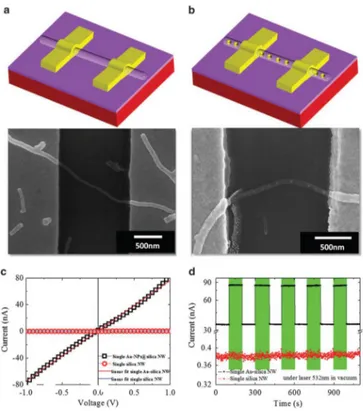
2. SiO2 Nanowires-Au Nanoparticles pea-podded: noble-metal nanoparticles encapsulated
in a dielectric matrix have attracted sustained interest over several centuries owing to their unusual optical and electrical properties. Metal-dielectric nanocomposites show non-linear and fast optical response near the SPR frequency due to their enhanced third-order optical susceptibilities [80]. Thus, they have been applied in optical switching devices [81, 82]. Several approaches, such as the sol-gel process, metal-dielectric co-sputtering deposition, metal-ion implantation into a dielectric matrix and pulsed laser deposition have been used to prepare metal-dielectric nanocomposites [83, 86]. In addition to the mentioned metal-dielectric nanocomposites that are mainly prepared in thin film or bulk forms, the one-dimensional noble-metal nanoparticle chain has become an intensive research focus because of its potential applications for nanoscale integrated optics below the diffraction limit of light. It has been suggested theoretically and experimentally that the electromagnetic energy can be transported below the diffraction limit by a coupled-plasmon mode in the linear chains of noble-metal
nanoparticles. The successful synthesis of a one-dimensional hybrid nanosystem known as a “peapod”, offers a promising opportunity to realize a wide variety of functionalities. The best-known example among them is the all-carbon hybrid peapod structure, consisting of fullerene molecules encapsulated in single-walled carbon nanotubes, which has been demonstrated to show several unusual physical properties.
In the paper of M.S. Hu et al. [80], it is reported the approach for fabricating a self-organized metal nanoparticle chain encapsulated in a dielectric nanowire with SPR-induced conductivity therein. Cathodoluminescence measurements on the gold nanopeapodded silica nanowires are carried out using a Gatan with an acceleration voltage of 8 keV. Figure 1.9 shows typical cathodoluminescence spectra of gold nanopeapodded silica nanowires at five different temperatures.
Figure 1.9 - Temperature-dependent cathodoluminescence spectra of gold nanopeapodded
silica nanowires. The inset shows the corresponding FTIR spectrum [80]
The authors highlight that the spectra are composed of three characteristic peaks at 1.9, 3.0, and 3.3 eV. The 1.9 eV band can be ascribed to the non-bridging oxygen hole centres or oxygen dangling bonds (≡Si–O) [87]. The 3.0 eV band corresponds to the two fold coordinated Si lone pair centres originating from the formation of strain bonds (≡Si–O–Si≡), when mechanical stress is applied to the silica glass [88, 89]. The 3.3 eV band may be correlated with the formation of the Si–O–C owing to the reaction between ≡Si–O defects and carbon atoms during nanowire growth, which has been reported in carbon-doped silica [90, 91]. As no carbon-containing gas reactants are intentionally introduced during nanowire growth, the authors suppose that the incorporated carbon might originate from the sputtering process of gold thin films under ambient air or the residual contaminant in their reaction chamber. Analyses of bonding configurations from Fourier transform infrared (FTIR) data also confirm the existence of Si–O–C and ≡Si–O–Si≡ (fig. 1.11, inset) .
31
Ultraviolet-visible absorption measurements are performed on a set of the composite nanowires grown on quartz substrate with different gold filling in the silica nanowires. The room-temperature ultraviolet-visible absorption spectra for plain silica nanowires (dotted line), gold-peapodded silica nanowires (solid line) and gold-filled silica nanowires, wherein the gold segments show an aspect ratio of 3-5 (dashed line), are shown in fig. 1.10
Figure 1.10 - Optical absorption spectra for plain silica nanowires (dotted line), gold
peapodded silica nanowires (solid line) and gold-filled silica nanowires wherein the aspect ratio of the gold segment is about 3-5 (dashed line)[80].
The gold-filled and gold-peapodded silica nanowires reveal a pronounced SPR absorption band at 532 nm, whereas the plain silica nanowires do not show any SPR absorption. The SPR band at 532 nm is attributed to the transverse plasmon mode, and the longer wavelength band is associated with the longitudinal plasmon mode [92], which was observed for composite nanowires containing gold segments of high aspect ratio (see the dashed line in fig. 1.10 (b)). The absence of the longitudinal mode in the gold-peapodded nanowires (see the solid line in fig. 1.10 (b)) may be ascribed to the small aspect ratio (<1.2) of the gold nanoparticles. The observed background in the composite nanowires originates from an interband transition of valence electrons to the Fermi surface.
Photoresponse measurements based on the nanowire ensemble devices are conducted under alternate light illumination of different wavelengths and under dark conditions.
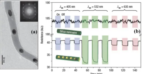
Figure 1.11 – (a) TEM images showing the structure of metal nanoparticles encapsulated
silicon dioxide nanowire. The inset in in fig. (a) shows an electron-diffraction pattern recorded along the [120] zone axis. (b) Photoresponse measurements. The room-temperature resistance response as a function of time to light illumination for plain silica nanowires (upper part) and gold nanopeapodded silica nanowires (lower part). Shaded (pink, excitation wavelength lex =635 nm; green, lex =532 nm; purple, lex =405 nm) and unshaded regions mark the light-on and light-off periods [80].
The resistance of the hybrid peapod nanowire device shows nearly a five times smaller value than its counterpart without gold nanoparticles. More interestingly, the hybrid peapod nanowire device presents a wavelength-dependent photoresponse in resistance. The photoresponse behaviour at a SPR wavelength of 532 nm shows a larger difference in resistance between the illumination on and off conditions (fig. 1.11). The resistance change is nearly five times that observed using 632 and 405 nm light. Furthermore, an excitation-intensity-dependent resistance is measured using 532 nm light at various pumping powers. M.S. Hu et al. believe that the enhanced photosensitive behaviour observed from the hybrid nanowire device can be attributed to the SPR, as the hybrid nanowires have a pronounced SPR absorption at 532 nm. The enhancement of photoresponse behaviour arising from the excitation of the surface plasmon has been reported for metal-oxide-metal (MOM) tunnelling junctions, which is attributed to the generation of hot electrons owing to the decay of surface plasmon polaritons. The generated hot electrons drift or diffuse to the oxide barrier, and tunnel to the counter electrode. In the case of their study, one-dimensional gold nanopeapodded silica nanowire can be regarded as an MOM tunnelling junction in series. The generation of hot electrons and electron tunnelling through the oxide nanowires may contribute to the enhanced photoresponse behaviour in our hybrid nanowire. The authors suggest that this simple one-step approach could be extended to the preparation of other metal-dielectric peapod-type nanowires with different functionalities. Basides, SiO2 NW-Au NPs composite systems are gaining a great scientific and technological
33
optical devices and sensors. In particular, these pea-podded structures are used as light waveguides or biosensors, in line with the results reported by Wang et. al. [93]. The authors report SP resonance enhanced molecular oxygen sensing by single Au NPs-SiOx NW under 532-nm illumination (visible light) at room temperature. Moreover, excellent selectivity of Au NPs-SiOx NWs to molecular oxygen in air has been demonstrated. To understand the electrical and opelectronic properties, they report the current-voltage (I-V) charactersistics, measured at room temperature in vacuum.
As shown in figure 1.12 (c), the I-V plots of both NWs are linear, indicating the ohmic nature of the e-beam defined contacts.
Figure 1.12 - Field-emission scanning electron microscopy images of single NW devices
consisting of (a) plain silica NW (without the Au NPs) and (b) Au-NPs@silica NW. (c) Dark I–V characteristics of single NW devices, with and without Au NP peapods, measured in vacuum, and the corresponding linear fit to the data set. (d) Dark and photocurrent measured under vacuum in single NW devices, with and without Au NP peapods, as a function of time. The color bars indicate the duration of the 532-nm illumination. The measurement has been performed with a 1 V applied bias at room temperature. The bare silica NW showed no photoresponse, whereas the Au-NP@Silica NW showed strong photoresponse [93].
The slope of the I-V plot indicates that the electrical conductivity of the Au NPs-silica NW is higher than that of the bare silica NW. This trend occurs for the creation of more electron-hopping sites in the Au-NPs-silica NW leads to enhanced conductivity [94]. During the growth of Au NP-peapodded silica NWs, residual Au atoms may partially incorporate into the silica matrix of the wire during the peapod formation [80]. The incorporation of Au may produce impurities and/or defect-related hopping sites in the silica matrix [94].
The Au-embedded silica NW has higher conductivity than the plain silica NW, because of its shorter hopping length. Photoresponse measurements of the NW devices, conducted under alternating 532 nm illumination and dark conditions, is shown in figure 1.12 (d).
The plain silica NW device does not show any significant photoresponse; the ratio of photo and dark current is ~0.01. In contrast, the Au NPs-silica NW device presents a reversible photoresponse and a stable photocurrent, with a photo/dark current ratio of ~1.48. Assuming the band gap of silica NWs to be in the range of ~6.8 eV [95], and denying any absorption of the 532 nm light, these data suggest that the photocurrent can be attributed to the near-resonance SP absorption of the Au NPs (within the silica NWs) that has been reported at ~532nm [80]. Taking into account these optoelectronic properties, such complex systemscan be used as light waveguide. Indeed, the resonant coupling between the incident light and the plasmonic resonances of Au NPs can induce an enhancement of the output signal.
Taking into account the necessity to modulate the plasmonic properties for each specific application, in the following chapters the results of the synthesis and characterization of metallic nanostructures with complex shape and composition are reported.
Besides, the correlation between structural and optical parameters of other complex shape and composition metal nanostructures (gold nanoring and ring dimmers, disk dimmers, hematite-Au core-shell nanorice particles, nanoporous (np) gold film, np-Au nanowires and np-nano pillars structures) are reported in the appendix to this chapter.
35
References
[1] Fahlman BD., Mat. Chem., Vol. 1. Springer; Mount Pleasant, p. 282-283 (2007) [2]Younan Xia, Yujie Xiong, Byungkwon Lim, Sara E. Skrabalak -Angew Chem Int Ed Engl.;
48(1): 60–103 (2009)
[3] Halperin WP., Rev Mod Phys., 58:533 (1986)
[4] Bawendi MG, Steigerwald ML, Brus LE. Annu Rev Phys Chem., 41:477 (1990) [5] Weller H. Adv Mater., 5:88(1993)
[6] Alivisatos AP. Science., 271:933(1996)
[7] Murray CB, Kagan CR, Bawendi MG., Annu Rev Mater Sci. 30:545 (2000); [8] Maheshwari V, Kane J, Saraf R. Adv Mater., 20:284 (2008)
[9] Mott NF. Rev Mod Phys., 40:677 (1968)
[10] Markovich G, Collier CP, Henrichs SE, Remacle F, Levine RD, Heath JR. Acc Chem Res., 32:415 (1999)
[11] Jeong U, Teng X, Wang Y, Yang H, Xia Y. Adv Mater., 19:33(2007) [12] Angew Chem Int Ed Engl. 48(1): 60–103 (2009)
[13] Lewis LN. Chem Rev., 93:2693(1993)
[14] Davey NM, Seymour RJ. Platinum Met Rev., 29:2 (1985) [15]Hamilton JF. Adv Phys., 37:359 (1988)
[16] Murray CB, Sun S, Doyle H, Betley T. MRS Bull., 26:985 (2001) [17] Murray CB, Sun S, Doyle H, Betley T. MRS Bull., 26:985(2001)
[18] Maier SA, Brongersma ML, Kik PG, Meltzer S, Requicha AAG, Atwater HA., Adv Mater. 13:1501 (2001)
[19] Sanders AW, Routenberg DA, Wiley BJ, Xia Y, Dufresne ER, Reed MA. Nano Lett. 6:1822 (2006)
[20] Taton TA, Mirkin CA, Letsinger RL. Science. 289:1757 (2000);
[21] Chen J, Saeki F, Wiley BJ, Cang H, Cobb MJ, Li ZY, Au L, Zhang H, Kimmey MB, Li X, Xia Y. Nano Lett. 5:473 (2005)
[22]West JL, Halas NJ. Annu. Rev. Biom. Eng. (2003)
[23] Kottmann JP, Martin OJF, Smith DR, Schultz S. Phys. Rev B. 64:235–402 (2001) [24] Valden M, Lai X, Goodman DW. Science. 281:1647 (1998)
[25] Narayanan R, El-Sayed MA. J Phys Chem B. 109:12663 (2005) [26]Falicov LM, Somorjai GA. Proc Natl Acad Sci. 82:2207 (1985)
[27] Xia, Y., Xiong, Y., Lim, B., and Skrabalak, S.E. Angew. Chem., Int. Ed., 48 (1), 60–103. 2 (2009)
[28] Elechiguerra J.L., Reyes-Gasga J., and Yacaman M.J., J. Mater. Chem., 16 (40), 3906v (2006).
[29] Zhang J., Langille M.R., and Mirkin C.A., J. Am. Chem. Soc., 132 (35), 12502–12510 (2010)