POLITECNICO DI MILANO
Scuola di Ingegneria Industriale e dell'Informazione
Corso di Laurea Magistrale in Ingegneria Meccanica e
Ingegneria dei Materiali e delle Nanotecnologie
3D-Printed Titanium Accelerometers
Relatori: Alberto Corigliano Riccardo Casati Emanuele Zappa Valentina Zega
Tesi di Laurea di:
Luca MARTINELLI Matr. 853267
Contents
Introduzione 1
1 Additive Manufacturing for Sensors and MEMS 3
1.1 Additive Manufacturing . . . 5
1.2 AM Advantages for Manufacturing Sensors . . . 5
1.3 AM future trends . . . 6
2 Metal 3D printing 9 2.1 Selective Laser Melting (SLM) Overview . . . 9
2.2 SLM Printing Process . . . 10
2.3 Distorsions and Residual Stresses . . . 10
2.4 Internal Porosity . . . 12
2.5 Surface Roughness . . . 13
2.6 Alloy Microstructure . . . 13
2.7 Heat Treatment . . . 15
2.8 SLM key takeaways . . . 15
3 Design and Fabrication of 3D-Printed Accelerometers 17 3.1 Cantilever Combs . . . 17
3.2 Biaxial Accelerometer . . . 18
3.3 Capacitive Accelerometers . . . 21
3.4 3D-printing Fabrication . . . 24
4 Experiments on the Fabricated Devices 27 4.1 Instruments Setup . . . 27
4.1.1 Shaker . . . 27
4.1.2 High-Speed Camera . . . 28
4.1.3 Image Pattern Matching . . . 28
4.1.4 Sound Spectral Analysis . . . 29
4.2 Cantilever Combs . . . 29
4.2.1 Random Excitation Shaker Test . . . 29
4.2.2 Resonance Excitation Shaker Test . . . 31
4.3 Biaxial Accelerometer . . . 34
4.4 Capacitive Accelerometer . . . 35
4.4.1 Mechanical Tests . . . 35
4.4.2 Capacitive Tests . . . 35 iii
iv CONTENTS 5 Material Characterization 39 5.1 Cross-Section analysis . . . 39 5.2 Surface Inspection . . . 41 Conclusions 43 Bibliography 45 Riferimenti citati nel testo . . . 45
Pubblicazioni e Manuali . . . 45
Materiale Online . . . 46
Ulteriore materiale consultato . . . 46
Pubblicazioni e Manuali . . . 46
List of Figures
1.1 SEM image of a typical silicon MEMS accelerometer [4] . . . 3
1.2 Example of a typical photolithograpic process for MEMS fabrication [4] . . . 4
2.1 SLM printing process illustration [3] . . . 11
2.2 Thermal deformations in one of our sensors . . . 12
2.3 SEM images of the as-built surface, printing direction is left to right 14 2.4 Ti-6Al-4V microstructure [6] . . . 14
3.1 Cantilever beam lengths. . . 18
3.2 CAD model of one of the cantilever combs (84.1 x 46.5 x 15mm), beam thickness 1.5 mm, all devices were printed in the out-of-plame direction . . . 18
3.3 CAD model of the biaxial sensor. Outer frame is fixed, inner frame can move vertically, center mass can move horizontally with respect to the inner frame. All our devices are printed in the Z direction . . 19
3.4 Von Mises equivalent stress (MPa per 1g of acceleration) in the Biaxial Device . . . 20
3.5 Folded beam with anchoring points. . . 20
3.6 Basic Capacitive Accelerometer diagram . . . 22
3.7 Differential capacitive accelerometer diagram . . . 23
3.8 Capacitive accelerometer parts to be assembled (not to scale) . . . . 23
3.9 CAD model of the capacitive sensor . . . 23
3.10 Assembled capacitive sensor with electrical connections and FEM computed Von Mises equivalent stresses (MPa for 1g acceleration) . 24 3.11 Renishaw AM250 printing the samples . . . 25
3.12 All the as-built sensors and cantilever combs, 15cm ruler for scale . 25 3.13 A belt saw separating the printed samples from the titanium base . 26 4.1 A cantilever comb mounted on the shaker and MIKROTRON camera 27 4.2 A captured frame and NI pattern matching algorithm at work . . . 28
4.3 "Spectrum" app, picking up the difference between a 350Hz and a 360Hz pure sinusoidal computer generated noise . . . 29
4.4 FFT of the average position of the bases . . . 30
4.5 spectra of 1.5mm thick cantilevers under random excitation . . . 31
4.6 Resonance frequency table: theoretical design value, shaker excita-tion frequency during resonance testing, FFT of camera recorded displacements, and sound spectrum peak frequency . . . 32
vi LIST OF FIGURES 4.7 TODO: FIX THIS TABLE . . . 32 4.8 Measured Frequency and Q factors for all cantilever combs and the
three sensors (2 modes of the biaxial and 2 identical capacitive sensors 33 4.9 Cantilever Amplitude Decay . . . 34 4.10 Captured frames of the biaxial sensor excited in two perpendicular
directions, 303.5Hz resonance (left) and 337.5Hz (right) . . . 34 4.11 Captured frame of the capacitive sensor during testing . . . 35 4.12 Capacity meter measurements . . . 36 4.13 Measured FRF exciting the sensor with one capacitor, while sensing
the other . . . 37 4.14 Sensor mounted on a support board and connected to the MEMS
characterization workstation . . . 37 4.15 Differential capacitance (top) and the two separated capacities
mea-sured at rest (bottom) . . . 38 5.1 Automatic diamond grinding wheel cutting a cross section sample
(left), polished cross sections (right) . . . 39 5.2 Optical microscope composed images of the three beams. from the
top, 0.5mm, 0.6mm and 1.5mm design thickness . . . 40 5.3 Measurement of the actual thickness, in order 377, 463 and 1386 µm 40 5.4 SEM images of typical lack of fusion defect and two internal porosities,
back scattered electrons (right) and secondary electrons (left) . . . . 41 5.5 SEM images of the as-built surface, printing direction is left to right 41
Abstract
This thesis work focuses on the design and fabrication of centimeter-sized 3D printed accelerometer prototypes. A general overview of the involved Selective Laser Melting technology is provided, as well as the expected properties of the printed material. Six pieces were fabricated in total: three arrays of cantilever beams and three accelerometers. The cantilevers mechanical response was used to better understand the material behavior, while the accelerometers can be considered a first attempt to make a functioning sensor. After the main geometry design choices are laid out, experimental test and results are discussed. Sensor excitation was provided by a mechanical shaker, while displacement measurements were carried out by a high speed camera. Once tests were completed, cross sections of the cantilever beams were cut out, polished and examined under a SEM microscope. An initial device underperformance was found to be caused by a reduced effective cross section of the 3D printed springs. Future works will likely need to compensate for this reduction in the design steps.
Keywords: MEMS, Accelerometer, Additive Manufacturing, 3Dprinting, Titanium
Introduction
With the growing interest in 3D-printing techniques to manufacture increasingly complex and detailed metal parts, we thought it might be of interest to push the limits of this technology and see how far we could get in the attempt to make a MEMS 3D-Printed with metal.
Of course current technological limitations prevent us from reaching the microscale, but making accelerometric devices only a couple of centimeters in size is here proven to be doable with the means currently at our disposal.
In this thesis we will explain the design choices made, the limitations encoun-tered and the results obtained during this endeavor.
Currently, manufacturing technologies for MEMS impose many restrictions on the development of new sensors, ranging from geometric limitations to long fabrication times for prototypes. The field is showing great interest for additive manufactur-ing as a tool to overcome these challenges and to add more flexibility to the industry. Of course, 3D printing should not be seen as a silver bullet against all these problems. It comes with its own set of challenges that we will proceed to outline. With this in mind, we would like to help laying the foundations for future works on 3D-printed sensors.
By studying the mechanical responses of small devices we hope we can provide a meaningful contribution to the characterization of the material at these scales and, in doing so, to ease the design stage of future projects.
2 Introduction
Outline
In the first chapters we give a general outline for MEMS sensors and current tecnology limitations to their manufacture, we discuss what contributions 3D print-ing can offer to this field as well as its own limitprint-ing factors.
In the following chapters, we delve into the details of SLM metal 3D printing technology, its advantages and shortcomings compared to traditional fabrication processes. For the purposes of this thesis work, we focus only on Ti-6Al-4V tita-nium alloy, explaining why additive manufacturing of this material is of particular commercial interest.
Afterwards, we explain the design process behind our printed accelerometers, the target sensitivity and the choice of geometric parameters to achieve that goal. We then proceed to describe the experimental setup, the tests that were car-ried out, and the significance of the obtained results. An unusual material behavior was identified during these tests, prompting us to investigate the internal structure of the 3D printed accelerometer springs.
Cross sections were taken from beams of different thickness and examined un-der optical and SEM microscopes, the results of these material characterizations will be very valuable if similar projects are to be attempted in the future.
In the conclusions, we outline reasonable objectives for said future attempt and succintly summarize the most meaningful findings of our work. ———————— —————–
Chapter 1
Additive Manufacturing for Sensors
and MEMS
Micro-electromechanical systems (MEMS) are micro devices combining mechan-ical and electro-mechanmechan-ical elements (typmechan-ically range approximately from 1 to 100 microns in size), that involve the conversion of a measured mechanical signal into a machine readable signal which could be optical, electrical, or thermal.
Initially, MEMS was developed for various applications such as pressure and temperature sensors, gas chromatographs, accelerometers, and switches for low-frequency applications. Over the past few decades, MEMS have become an integral part of several research areas such as optics, biomedical devices, therapeutic strate-gies, mechanical, electrical, and aerospace studies. Some of the current MEMS
Figure 1.1: SEM image of a typical silicon MEMS accelerometer [4]
devices include digital light processing for projectors, micro-gyroscopes within cellphone packages, accelerometers and pressure sensors within automotives, lab-on-a-chip DNA diagnostic toolkits, gas sensors for a variety of environmental, aerospace
4 Chapter 1. Additive Manufacturing for Sensors and MEMS and mobility applications, radio frequency MEMS, and optoelectronics. Generally, a typical MEMS device consists of four components, namely a micro-sized platform, sensing elements, micro-sized actuators, and microelectronics for control or data handling.[8]
Typical MEMS Manufacture
MEMS devices are fabricated using conventional technologies such as surface micromachining, bulk micromachining, Lithographie, Galvanoformung, Abformung (LIGA), wet/dry reactive etching, ultraviolet (UV) photolithography, metal
depo-sition schemes, chemical vapor depodepo-sition (CVD) processes, wafer bonding and packaging technologies, and electroplating. These techniques are based on additive
Figure 1.2: Example of a typical photolithograpic process for MEMS fabrication [4] or subtractive processes that handle precise and miniscule volumes of materials in the form of thin layers on surface of silicon wafers. These traditional methods are highly precise and suitable for fabrication of planar geometries.
For fabrication of MEMS devices with high aspect ratios, wet etching and deep reactive ion etching processes are used where 3D features are created on stacked silicon wafers. Albeit the precision, these processes are associated with certain
1.1. Additive Manufacturing 5 drawbacks such as process complexity, heavy geometric limitations for 3D designs, requirement of specialized facilities and equipment, sophisticated work environment, high lead time, and incompatibility with some flexible materials (polymers and plastics). The emergence of these challenges has opened a window for the MEMS community to explore alternative 3D microfabrication strategies. The past decade has seen a significant increase in the utilization of AM technologies in MEMS fabrication in devices such as supercapacitors, resistors, inductors, microchannels, electronic printed circuitry, and sensor platforms. [8]
1.1
Additive Manufacturing
3D printing enables the creation of complex geometric shapes and merging of selected functional components into any configuration, thus supplying a new approach for the fabrication of multifunctional end-use devices that can potentially combine optical, chemical, electronic, electromagnetic, fluidic, thermal and acoustic features.
With the development of micro-machinery and advances in micro-controller plat-forms, elaborate sensors have been widely applied in manufacturing and machinery, aerospace and airplanes, medicine and biomedical devices, and robotics.
In recent years, a considerable amount of current research on 3D-printed sensors has focused on selected areas such as electronics, force, motion, hearing, optics, etc. Electronic and force sensing modules are particularly well suited for 3D printing, and other sensing categories tend to be manufactured by the integration of commercial components into 3D-printed structures.
Printed sensors combine several important technologies, such as printing tech-nology and electronic device design. [10]
Measurement of different parameters such as force, displacement, pressure, and strain is one of the most important necessities in engineering. In this regard, great care has been taken in their production, over the years. In this respect, different manufacturing processes are used for fabrication of sensors. For example, lamination, coating, and lithography are used for manufacturing of strainsensors. [7]
1.2
AM Advantages for Manufacturing Sensors
AM has proved its capabilities with great potential for changing fabrication of sensors, mainly due to several traditional manufacturing processes showing drawbacks in fabrication of electronics. For instance, expensive production of high resolution engineering components, limited scalability and time consuming processes are examples of these deficiencies. As advantages of 3D printing technology (e.g. fast fabrication and high accuracy) have been proved in various applications, it has drawn increasing interest that can be used for fabrication of different sensors.
The flexibility and versatility needed in 3D printing technology makes it very promising in fabrication of prototypes. In fabrication of a 3D-printed sensors, electronic device design and printing technology must be combined. This combina-tion needs expertise and knowledge in mechanics, electronics and material science.
6 Chapter 1. Additive Manufacturing for Sensors and MEMS Different aspects have crucial roles in developments of the sensors. For example, nanomotors, material combinations and biomimetic design showed their primary roles in printing of sensors.[7]
Limitations
Restriction of material in each 3D printing technique can be considered as a challenge in this rapid prototyping process. For instance, in Vat Photopolymer-ization (VP) technique, photocurable polymer must be used, while filament type materials are needed in Fused Deposition Modeling (FDM) process. This material limitation has influences on the performance and reliability of the printed sensors. In fact, the limitation in existing printable materials need further development to improve fabrication of 3D-printed sensors.
Another challenge in production of 3D-printed sensors refers to the life cycle of these engineering components. As 3D-printed sensors are relatively new, and they are not used for many years, there is no information about problems of their durability. In order to survey life cycle of the 3D-printed sensors, every production step must be considered. In this context, importance of this assessment depends on the particular application of the printed sensor. Since waste from electronic devices is one ofthe largest waste categories, it is concluded that lifetime of the electronic devices are rather short. Short lifetime means the consumption of the products could be high. In this regard, if 3D printing leads to production of sensors with short lifetime, increase in the quantity of future waste is expected. [7]
1.3
AM future trends
Since different properties of 3D-printed sensors can be adjusted via changing and optimizing printing parameters, future researches should consider the potential effects of these parameters precisely. For example, variation in the printing speed can lead to a change in linewidth of the 3D-printed sensor. In this regard, requiring specialized equipment should be avoided which is considered as a disadvantage in this rapid prototyping process. Utilizing 3D printing technology in fabrication of sensors is still requiring technical research and development. The expectations are high in future applications of 3D-printed sensor, due to the increasing demands in engineering and medicine fields. Development in biodegradable materials for the sensors, improving adhesive connection of 3D-printed parts, and new methods of printing with higher resolutions are examples of research themes that can be studied in future research and development. Moreover, because of using nanomaterials in 3D-printed sensors, questions about recycling of nanowaste needs to be answered in future studies.
Although the recent emergence of 3D printing techniques has opened new prospects in fabrication of different sensors, based on the existing challenges, further researches are needed. It is suggested to study physical, chemical and geometrical effects of 3D-printed sensors on their performance. This study can be in combination or separately. Moreover, deeper understanding and comparison of the 3D printing methods in fabrication of the same sensor is still missing. In this respect, various
1.3. AM future trends 7 parameters such as productivity, environmental influence, and performance of the methods must be evaluated. [7]
Chapter 2
Metal 3D printing
Also known in the past as Rapid Prototyping, Additive Manufacturing is an umbrella term that covers many technologies capable of constructing a three dimensional object starting from a digital 3D model. This can happen by material deposition, solidification, chemical reactions or other processes, typically one layer at a time. The main advantage brought by this technology is the ability to print previously impossible geometries or interlocking parts, but the technology comes with some important drawbacks. First of all, the printed materials often show anisotropic behavior (due to the nature of the layer-by-layer deposition process), possible internal porosities, high surface roughness and decreased fatigue life. [10] Some of these drawbacks can be attenuated with finishing techniques such as high pressure heat treatments, sand blasting or UV curing for polymers. Currently, minimum feature size is in the order of 0.1 − 0.5mm for most 3D printing technologies, with relatively few peculiar outliers such as two-photon lithography [0]. The technology used in this thesis work is Selective Laser Melting (SLM) technology of Ti-6Al-4V titanium alloy, for this reason we will mainly focus on this area for the rest of this chapter, while keeping in mind that other technologies face similar challenges.
2.1
Selective Laser Melting (SLM) Overview
When it comes to metal 3D printing, selective laser melting offers the opportunity to realise the best possible resolution and geometric complexity. SLM has the capability to fabricate intricate structures up to 0.1mm in thickness having surface roughness as low as 10µm, dimensional accuracy of 0.04mm, and part densities up to 99.99%
Since the geometric limitations on the part design are minimal, SLM can theoretically offer the full benefits of topology optimisation, allowing for remarkable weight savings. That being said, there are still certain complexities which demand more comprehensive research and understanding of the micro-scale physics as well as its impact on the macro-scale material properties and defects such as porosity, distortions, and anisotropy in mechanical properties. These defects play a critical role in load-bearing applications, especially when fatigue life is considered.
One area which can improve the quality of AM metal parts but lacks rules and 9
10 Chapter 2. Metal 3D printing guidelines is the geometric sensitivities to distortions, residual stresses, porosity, surface roughness, microstructural variation, and the possibility of build failure. Traditional design practices for 3D printing involves topology, shape and size optimisation with minimal regard to the influence of resulting geometry on the aforementioned characteristics of part quality. The research community has worked on the finite element modelling of the SLM process and have successfully estimated induced residual stresses [5]
2.2
SLM Printing Process
Like other similar powder bed melting processes, the printing happens one layer at a time. The powder (20 − 60µm in diameter) is evenly dispersed by a blade and subsequently melted by a laser, scanning along an algoritmically determined path. Often times this path is optimized to minimize the thermal deformations in the finished piece, for example by changing direction with respect to the layer below or compared to neighboring regions. The atmosphere during the printing process must be closely controlled to prevent oxidation, also an adequate flow of inert gas (Argon) is needed for blowing away metal spatter generated by the intense melting process. The powder bed is heated typically between 100°C and 400°C to prevent thermal shocks and reduce the needed laser power flow.
It is always advisable to add metal supports under any metal 3D-printed part, this is mainly done to increase the heat removal rate from the freshly printed region, which would otherwise happen too slowly through the powder and could worsen residual stresses in the final piece. This is especially true for titanium, which has a rather low heat conductivity compared to iron or copper, 4 and 23 times lower respectively.
Overhanging structures are especially challenging to print, since the lack of supports make the heat diffusion rather slow. Often times it is advisable to avoid unsupported overhangs in the design stage in favor of 45° leaning structures instead.
An optimal combination of printing parameters is often hard to achieve, since it involves many tradeoffs that will be discussed in the following sections.
2.3
Distorsions and Residual Stresses
Geometric features play a critical role in residual stress buildup and stress-induced deformations. Residual stresses in some instances, can even result in distortions high enough to cause build failures; this usually occurs in the case of weak supports. On an average for conventional AM materials such as Ti-6Al-4V, residual stresses are found to be two times larger in the scan vector direction. To overcome this directional anisotropy short scan vectors are levied, and scanning patterns are usually rotated between the layers to create a more homogeneous stress distribution. This methodology to limit part distortions has been experimentally proven and is extensively applied. As for the powder material used, residual stresses significantly depend on the in-process microstructure development and phase transformations which to a certain extent also depend on the part geometry, as thermal gradients vary with geometry and influence the phase transformation.
2.3. Distorsions and Residual Stresses 11
Figure 2.1: SLM printing process illustration [3]
All powder-bed fusion AM techniques operate via a layer-by-layer material addition, in the case of SLM, a laser beam of high energy density is used to melt the newly added layers. After laser irradiation, the molten material cools down rapidly, owing to the high heat conduction of the base plate and its relatively lower temperatures, inducing a shrinkage tendency in the added layer. This shrinkage is inhibited by the underlying material resulting in plastic and elastic strains at the interface of the part and the added layer. It is quite intuitive to visualise that the resulting strains to a large extent would be controlled by the thermal gradients and the structural strength of the underlying material to inhibit these shrinkage tendencies.
Mercelis and Kruth [9] suggested that for the conventional AM materials such as Ti-6Al-4V, resulting strains in the topmost layers are tensile in nature and equivalent to the material’s yield strength. However, as mentioned previously, this is not the case for materials which undergo martensite transformations.
The internal stress state of the build changes with the addition of each subsequent layer consequently, small deformations take place throughout the part and build plate to accommodate the new stress state, and equilibrium of residual stresses is maintained throughout the process. In some instances, localised stresses can reach a high enough value to cause significant deformations leading to building failure. Some of the measures to prevent these failures are to avoid thin and weak members that potentially act as support for the subsequent layers; such geometries are unable to withstand the high residual stresses. Once fabrication is complete, the printed parts are separated from the build plate, which causes the stresses to relax and is usually accompanied by noticeable deformations. Along with residual stresses, these deformations also depend on the stiffness of the part.
Regulating post-build distortions is quite crucial in most of the structural applications. . It is a common practice to either simulate the build or experimentally obtain the distortions to estimate the printing accuracy for individual designs. Some
12 Chapter 2. Metal 3D printing of the critical guidelines to avoid build failures and to minimise part distortions are listed below. Stress induced deformations can be compensated for in the design stage, finite element simulations are also used to predict the as-built distortions which are then inverted to obtain a modified part geometry that allows for processinduced distortions. [2]
Figure 2.2: Thermal deformations in one of our sensors
2.4
Internal Porosity
Limiting part porosity is essential for material integrity, especially in structural applications susceptible to fatigue loading. AM metal components show a high vari-ation in the shape and size of pores, which makes it sometimes difficult to estimate the effect of net porosity on structural strength. Apart from the conventionally optimised parameters like laser power and scan speed, porosity also depends on the thermal gradients, layer thickness, powder size, and part geometry.
Porosity in laser melted 3D parts primarily consists of gas bubbles trapped within the melt-pool (keyhole defects) and un-melted powder also characterised as lack of fusion defects. An increase in lack of fusion porosity was observed with increasing laser speeds, reducing melt-pool size or the decreased peak temperature.
It is well known that thermal gradients, for a specific set of process parameters, necessarily depend on the underlying geometry. It can be readily seen that even slight changes in build orientation can significantly alter the porosity distribution within the part.
These porosity defects thus have a high probability of being the source of crack initiation sites. For tensile test specimens built horizontally, such defects would
2.5. Surface Roughness 13 have their sharp edge in-plane of the applied load and would consequently be less critical
Even for a set of optimum process parameters, it could be challenging to eliminate the porosity defects. Mainly because the porosity defects lie on the opposite spectrum of the optimal process window that is, high energy densities result in keyhole pores and low energy densities lead to lack of fusion defects. Hence, severe changes in thermal gradients, which are bound to occur in complex geometries, could result in either keyhole or lack of fusion porosity.
Considering the geometric dependence of porosity, certain design practices can help reduce its occurrence or at the very least limit the adverse effects of porosity on the resulting structural strength.
Optimise laser density: geometries with the tendency to rapidly cool down would favour lack of fusion porosity.
Optimise build orientation: anisotropy in structural strength due to lack of fusion defects should be given critical thought when designing complex geometries.
Provide generous radii: generous radii at the interface of part/substrate platform would prevent the part from stripping off during manufacturing as well as provide a subtle transition in thermal gradients and would ultimately result in higher densities.
Plan an effective tool path: poor tool path planning results in the dwelling of the laser at the turnaround points. This increase in laser density can lead to keyhole defects. Further, if the bulk-fill laser paths do not intersect the contour passes, insufficient laser density can cause a lack of fusion. Both defects usually occur near the contour and result in subsurface porosity, which is detrimental to the structural integrity. These defects are particularly significant in thin members and can be controlled with appropriate scan strategy. [2]
2.5
Surface Roughness
Components susceptible to fatigue often have higher surface quality requirements as surface initiated cracking can lead to premature failure. Another requirement for good surface finish is to ensure part functionality and compatibility. It is for these reasons that many of the powder bed processes, sometimes require post-processing operations to reach acceptable levels of surface roughness. These operations may delay part completion and add to the production cost.
Surface roughness in selective laser melting processes predominatly depends on three of the following phenomena: thermal aspects that control the melt pool physics and affect the top surface roughness, presence of partially melted powder on the inclined, side and overhang features, and the layer thickness which introduces steps (staircase effect) in the inclined surfaces. [2]
2.6
Alloy Microstructure
SLM technology is characterized by fast cooling rates, directional heat flow and repeated thermal cycles. These factors have a strong influence on the microstructure,
14 Chapter 2. Metal 3D printing
Figure 2.3: SEM images of the as-built surface, printing direction is left to right thus SLM parts are characterized by the formation of metastable phases induced by rapid cooling rates (i.e. martensite), supersaturated solid solutions and preferential grain growth direction produced by the directional heat flow.
The pre-heating in SLM is considerably lower than other similar powder bed melting technologies, leading to even faster cooling rates. For Ti-6Al-4V, the microstructure typically obtained after SLM is an α fine acicular martensitic. More precisely, during printing we assist to the formation of columnar β grains aligned with the build direction that can encompass several layers due to epitaxial growth and, by cooling, these grains are filled by martensitic needles during the β to α decomposition.
Figure 2.4: Ti-6Al-4V microstructure [6]
The final microstructure depends on the volume energy, i.e. the amount of heat received by the melt and the surrounding powder: less heat means faster cooling rates and thus a finer structure. Due to melting of successive layers one on top of the other, precipitation of Ti3Al can occur, as with ageing. In general, the microstructures obtained with SLM reflects a more or less fast cooling from a melt.[3]
2.7. Heat Treatment 15
2.7
Heat Treatment
The SLM as-built martensitic microstructure of Titanium is normally not suitable for many applications because, despite being hard and strong, displays low ductility. Moreover, there are high residual stresses that can cause distortions or even cracks. Post manufacturing stress relieving heat treatments are commonly carried out, from about 700°C (only stress relieve) to 1000°C (solution annealing). The latter completely decomposes the martensitic microstructure into the equilibrium α + β phases, and considerably coarsens the grains.
Hot isostatic pressing (HIP) is another common process, that consists in applying an hydrostatic pressure (by the means of a fluid, like oil) and simultaneously a high temperature (about 920°C): the effect is to transform the martensite into α + β and to close surface porosity and, consequently, increase ductility and fatigue resistance at the expense of a small decrease in strength.[3]
2.8
SLM key takeaways
For the residual stress and distortion defects, both the overall part geometry and localised features play a significant role. The thermal and structural aspects of the geometry, which govern the development of residual stresses were discussed, and design guidelines to limit these process-induced stresses were provided. Further-more, the residual stress development is unique to the material under consideration, but the geometric effects for these defects are similar for all the materials. The process-induced porosity defects also show a dependence on the part geometry. Further, the porosity found in laser AM components is partially responsible for the anisotropy in mechanical properties. Guidelines to control the porosity and improve material isotropy were provided. As far as the geometric aspects are considered, the surface quality mainly depends on the orientation of the external surfaces. This aspect of part quality is much more critical in designs with internal channels and lattice structures. Microstructure characteristics also show a geometric dependence. However, the extent of these defects and their relationship with geometric features are not documented well enough to provide specific design recommendations. To conclude, structural applications and certification requirements in both the auto-mobile and aerospace industry require high material integrity and consistency in the fabrication process. To ensure the same for SLM, not only process optimisation but also the part design should be given critical thought. The anisotropy found in SLM fabricated parts poses a risk to the material integrity and makes it harder to predict the structural performance for any complex design. Certain geometric features, being more susceptible to defects such as lack-of-fusion pores, variable microstructure and sharp notches from the poor surface quality, show a propensity for exacerbating the material anisotropy, making it crucial to explore the correlation between material anisotropy and geometric features. Development of computation-ally efficient simulation techniques to predict process-induced defects for complex geometries could be a pivotal addition to the iterative design optimisation methods. [2]
16 Chapter 2. Metal 3D printing in this field, it provides higher resolution than its main competitor Electron Beam Melting (EBM) and, unlike the latter, SLM does not need to operate under high vacuum regimes. More generally, the part complexity achievable with 3D-printing is truly remarkable, making it the ideal choice to fabricate topology-optimized parts, cellular solids, or simply for customized components. Its flexibility allows to fabricate prototypes at an unprecedented speed or to be employed job-shop production systems, where production volumes are low, components are not standardized, or need to be custom made.
From a more managerial perspective, 3D printing can also be useful in cutting down stockholding costs. Some types of seldomly requested spare parts could be printed on demand, instead of taking up warehouse space and inventory list for long periods of time.
Chapter 3
Design and Fabrication of
3D-Printed Accelerometers
For the duration of this thesis work only a single printing run could be performed, this was somewhat unfortunate because we had to design our accelerometers without characterizing the material at these small scales first. From a previous study conducted here at Politecnico di Milano [1], we had reasons to believe the material would under-perform when used to make sub-millimeter thin beams. This meant we had to proceed assuming the material would perform just the same way it does at larger scales and then draw conclusions from the observed deviancy. During the printing run, six pieces were printed in total: 3 combs of cantilevers and 3 accelerometers. The purpose of printing the cantilever combs was to investigate the behavior of the 3D-printed TiAl6V4 alloy, which is expected to change significantly depending on the thickness of the beams. The other three pieces were the accelerometric devices, respectively a 2-axis accelerometer and two identical capacitive accelerometers.
3.1
Cantilever Combs
As mentioned above, during a previous work at Politecnico di Milano a 3D-printed aluminum accelerometer behaved in unexpected ways. Namely, the measured resonance frequency was lower than the design value by a significant margin. This could be due to many causes: the remarkable thinness of the beam pushing the printer too close to its resolution limit, the presence of significantly sized defects in its cross-section, a reduced effective Young’s modulus due to porosity or other unknown factors. Furthermore, these aluminum devices fatigue-failed after a fairly low number of load cycles. 3D-printing with aluminum powder was not possible for the duration of this thesis work, so it was decided to investigate whether the available TiAl6V4 alloy behaved similarly. Three combs of cantilevers were designed (figure3.2, with their beam thicknesses set to 1.5mm, 0.6mm and 0.5mm respectively.
Each set had four beams of varying length, each meant to resonate at 250Hz, 350Hz, 450Hz and 550Hz. This was done using the resonance frequency of a cantilever beam:
18 Chapter 3. Design and Fabrication of 3D-Printed Accelerometers ω0 = s EJ α4 ρAl4 → l = α r t ω0 4 s E 12ρ
where α ≈ 1.875 is a pure number, E = 100GP a, ρ = 4.5g/cm3, J = ht3/12 = At2/12 is the second moment of area of the rectangular cross section and t is the beam thickness in the direction of oscillation. Results are reported in the table in figure3.1
Figure 3.1: Cantilever beam lengths.
Figure 3.2: CAD model of one of the cantilever combs (84.1 x 46.5 x 15mm), beam thickness 1.5 mm, all devices were printed in the out-of-plame direction Any significant deviation from these values would eventually provide insightful data for future designs and material characterization. The frame around the combs is mostly meant for protection against rough handling, but it can also resonate at 200Hz if needed. All three combs have the same height of 150mm which provide enough stiffness to prevent any significant out-of-plane motions.
3.2
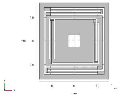
Biaxial Accelerometer
The main purpose of this accelerometer was to continue the work done by Giacomo Bonanomi [1] aimed toward testing the capabilities of our high-speed camera to detect sub-pixel displacements, at the same time it was used to gather more data to assess material behavior at small scales. The design aims to have two different resonance modes: at 420Hz for the inner springs and 400Hz for the outer springs. In theory an out-of-plane resonance mode is present, but for the purpose of
3.2. Biaxial Accelerometer 19
Figure 3.3: CAD model of the biaxial sensor. Outer frame is fixed, inner frame can move vertically, center mass can move horizontally with respect to the inner frame. All our devices are printed in the Z direction
this work it was considered undesired and the design has been made thick enough to push this mode above 1kHz, out of measuring range. After the general shape was decided, to adequately tune the geometric parameters of the accelerometer a simplified mass-spring analytical model was used, where stiffness was provided only by the suspended springs while the mass was provided by the moving parts.
For our sensors we often made use of a simple folded beam spring element (figure 3.5)
The stiffness of this element is quite simple to estimate with beam theory: it is composed of two beams of length l, if we approximate the folding point as infinitely rigid, we can aknowledge that both beams must esperience constant shear load, linear moment and, crucially, zero bending moment at their midspan. This means that the whole spring can be considered composed by 4 consecutive cantilevers of lenght l/2, each under a point load F at their tip. Their collective displacement is
δ = 4F (l/2) 3 3EJ → k0 = F/δ = 6EJ l3 = Eht3 2l3
where we used the second moment of inertia formula for a rectangular beam J = ht3/12, E = 100GP a is the material Young’s modulus, while l, t, h are the length, thickness and height of the beam respectively. The overall stiffness of the
20 Chapter 3. Design and Fabrication of 3D-Printed Accelerometers
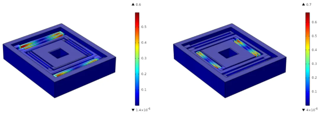
Figure 3.4: Von Mises equivalent stress (MPa per 1g of acceleration) in the Biaxial Device
Figure 3.5: Folded beam with anchoring points.
system k can be calculated by combining 2 of these folded springs in parallel k = 2k0 =
Eht3 l3
A more complete mathematical derivation of the mechanical model for folded beams can be found in the literature. [0]
The mass m was calculated from the geometry simply by assuming a material density ρ = 4.5g/cm3. Once the two are known, the resonance frequency omega
0 is just obtained with omega0 =pk/m. The 3D-printer allowed a minimum feature size of about 0.5mm, which was taken as the thickness t of the inner springs while the outer springs were arbitrarily set at twice as much, 1mm thickness, after a few trial attempts. The 0.5x0.5mm square hole in the middle serves both as an easily identifiable target for image pattern matching and as a target to shine a laser velocimeter in case the camera measurements did not provide significant data. After all these constrains were imposed, we took reasonable values for the leftover geometric parameters so that the resonance frequencies could be roughly estimated by: ω0 = pk/m = 2πf0. Afterwards, these parameters were taken as a starting point for the Microsoft Excel SOLVER module, which used gradient descent techniques to find the best-fit parameters that satisfied the two resonances (420Hz and 400Hz), as well as minimizing the overall accelerometer footprint. These parameters values were later fed to a COMSOL Multiphysics finite element model, in order to find a better estimations for the two natural frequencies. COMSOL disagreed with the Excel model by tens of Hz, so the COMSOL frequencies were
3.3. Capacitive Accelerometers 21 used to compensate the SOLVER "poor aim" and allowed Excel to provide better geometric parameters, which COMSOL disagreed less with. After a couple of COMSOL-Excel cycles, we found suitable geometric parameters for our final design.
3.3
Capacitive Accelerometers
During the preparation phase of this project, we grew curious whether it was possible to make a somewhat functional 3D-printed capacitive accelerometer sensor.
The simplest form of this kind of device generally consists in a mass suspended on springs (figure3.6). Applying a voltage difference between the mass and a nearby conductive plate will cause the two to act as a capacitor. Movement of the mass relatively to the plate will cause this capacitor gap to change, eventually leading to a detectable electronic signal. Whenever possible, more than one capacitor is used to create a stronger response.
In order to obtain a detectable change in capacity, our accelerometer had to satisfy many constraints. First of all, any basic capacitor needs two electrically insulated plates and a voltage difference applied between them. For us this meant that printing a monolithic capacitor would be a rather difficult task, since applying a voltage between two point of the same metallic object implies a short-circuit almost by definition. Instead we opted for a design which needed two copper plates to be manually attached afterwards. Layers of insulating material (PVC tape) were used to provide an appropriate capacitor gap. To find the needed design characteristics, data from a previous work at Politecnico di Milano were used [11]. Here the fabricated sensors showed a sensitivity of about 300fF per g of acceleration, we aimed our accelerometer to produce a signal of similar strength, so that we could be confident that most instruments were capable of picking it up. We expected significant deformations in the final accelerometer, mainly due to thermal stresses caused by the printing process. Because of this and the manual assembly of the copper plates we expected the gap to be somewhat uncertain, but we proceeded with an educated guess of 0.3mm. The needed area could then be roughly estimated by a quick calculation: first we again approximated our accelerometer to a mass attached to a mass-less spring,
From the formula of a simple two plates capacitor we get: C = ε0 A x → dC dx = −ε0 A x2
22 Chapter 3. Design and Fabrication of 3D-Printed Accelerometers
Figure 3.6: Basic Capacitive Accelerometer diagram
where C is the capacitance, A is the area of the capacitor plates, and x is the gap between them. Then, if we disregard the attraction between the capacitor plates, we can write the mechanical equilibrium just with the inertial force of the mass and reaction provided by the spring:
k(x − x0) + ma = 0 → x − x0 = − m ka → dx da = − m k ≡ − 1 ω2 0
where m is the mass, k is the spring stiffness, x is the displacement from the equilibrium position x0, and ω0 =
q k
m is just the natural resonance frequency of any simple undampened mass-spring harmonic system, therefore the sensitivity S is just S = dC da = dC dx dx da = ε0A x2ω2 0 → A = Sx 2ω2 0 ε0
The area A is what we are looking to minimize, because ultimately it will be responsible for how big our sensor needs to be. A strongly depends on the gap and the ω2
0 resonance frequency. This is not that surprising, since the resonance can be seen a measure of the "almost adimentional stiffness" of the system. Systems with lower resonance will be less rigid and will be subjected to greater displacements, which in turn cause greater changes in capacitance. We would like to keep this resonance as low as possible, but the lower we get and the more the material is stressed, or the longer and more folded our springs will need to be. After several attempt between 100 and 200Hz, we settled for a resonance of 200Hz, or ω0 = 2πf0 ≈ 1257rad/s. Inserting all the other values S = 300fF/g = 300fF/(9810mm/s2), x = 0.3mm, ε0 = 8.854f F/mmwe get: A = Sx 2ω2 0 ε0 ≈ 490mm2
In other terms, about a 22x22mm square will be needed. By opting for a differential capacitive accelerometer design, we could split this area between two capacitors.
3.3. Capacitive Accelerometers 23
Figure 3.7: Differential capacitive accelerometer diagram
Figure 3.8: Capacitive accelerometer parts to be assembled (not to scale)
We will need approximately the area of two 15x15mm squares. For each one of these capacitors, we expect the capacity to be on the order of: C = ε0Ax ≈ 7.2pF For an applied potential difference of ∆V = 10V , the attractive force between the plates will be on the order of: F = C∆V2
2x ≈ 1.2µN confirming that electrostatic effects are indeed negligible as we assumed. A minimum feature size of 0.5mm was again chosen due to the 3D printer resolution limit, and a very similar COMSOL-Excel SOLVER method was used to find a suitable set of geometric parameters.
Figure 3.9: CAD model of the capacitive sensor
Later on, two copper plates were cut to size, small pieces of 0.15mm thick PVC insulation tape were attached to the plates and layered on top of each other. This was done in order to adjust the gap between the deformed titanium surfaces and
24 Chapter 3. Design and Fabrication of 3D-Printed Accelerometers the copper plates in such a way that the final gap would be as uniform as possible. After this step, the PVC was firmly glued onto the titanium and three separate copper wires were soldered onto each part for the electrical connections. Due to
Figure 3.10: Assembled capacitive sensor with electrical connections and FEM computed Von Mises equivalent stresses (MPa for 1g acceleration)
the relatively large capacitor gap, the surface roughness of the 3D-printed titanium was not a significant problem for us. If future attempts are to be made, it may be advisable to use some chemical etching or polishing process in order to smooth the titanium rough surface and prevent accidental short-circuits between the plates.
3.4
3D-printing Fabrication
3D printing metal powder can vary in size and composition depending on the specific application, in our case we used 20 − 63µm TiAl6V4 powder to print all of our pieces. Layer thickness was set to 60µm.
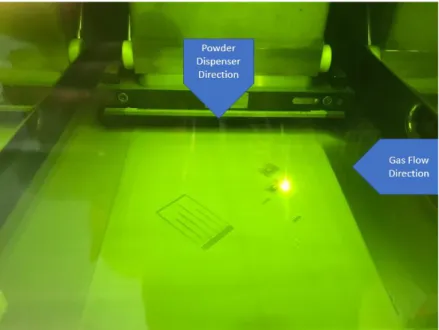
The 3D-printer used for this project was a RENISHAW AM250, the powder bed was heated to 150°C in a 21mBar oxygen deprived argon atmosphere. In this printer (figure 3.11) an inert gas flows from right to left in order to blow away metal spatters generated by the powder melting process. This prevents them to be included into following layers, but it is not an infallible method. It is usually a good practice not to position a piece downwind of another whenever possible.
The powder dispersing blade moves from top to bottom and it is advisable to orient edges at 45° with respect to it in order to minimize the risk of collisions. Bottom Supports
Under all parts we added 0.2mm thick - 1mm long - 2mm tall supports, pro-cedurally generated with Magics software and manually removed later. Supports firmly anchor the part to a titanium plate at the base of the printing chamber, this means that all parts need to be separated from the base plate. This step was done with a belt-saw. Many supports detached cleanly during this phase, while leftover supports needed to be removed manually with pliers and files. Being titanium a relatively hard metal, manual removal of the supports can become a rather difficult task, especially in hard to reach corners.
3.4. 3D-printing Fabrication 25
Figure 3.11: Renishaw AM250 printing the samples
26 Chapter 3. Design and Fabrication of 3D-Printed Accelerometers
Chapter 4
Experiments on the Fabricated
Devices
4.1
Instruments Setup
4.1.1
Shaker
The electromagnetic shaker was driven by its custom controller, which was in turn fed with a sinusoidal potential by a signal generator. Frequency was controlled by the generator, while amplitude was controlled by the driver. Two 1cm thick aluminum plates had been custom-made to firmly clamp each sensor and fix it to the shaker. An accelerometer was glued on top of this setup in order to record the
Figure 4.1: A cantilever comb mounted on the shaker and MIKROTRON camera accelerations the shaker is providing, as the shaker itself is not meant to gather data of any sort. Data from this accelerometer is aquired with the National Instruments module NI9234, this module can only sample at specific frequencies and here we
28 Chapter 4. Experiments on the Fabricated Devices mainly used a 10240Hz and a 5120Hz sampling rate, the high-speed camera sampled at these same frequencies, mostly for sake of consistency.
4.1.2
High-Speed Camera
For displacement measurements we used a MIKROTRON EoSens mini2 high-speed camera with ZEISS optics. Powerful LED lights were used to provide adequate illumination. Camera position, orientation, zoom and focus were slightly changed along the measurement process, but since we knew the approximate size of all geometric features of each design we could easily find how many pixels in the picture fit inside a real-life millimeter. It is worth noting that, when the camera is set up correctly, the main insurmountable bottleneck of the acquisition process is the data transfer from the CMOS sensor to the internal camera buffer memory. This means that the only way to achieve higher image sampling rates is to reduce the region of interest that has to be downloaded from the CCD sensor. All things considered, this translates to a trade-off between resolution and sampling rate. High-speed observation of a few seconds can produce many GigaBytes worth of 8-bit images, we found that for this large kind of image archives 7-zip provides a four times better compression ratios than Winrar or Zip folders, but the best way to handle this volume of data is to probably analyze it immediately after acquisition and avoiding long-term storage.
4.1.3
Image Pattern Matching
Object displacements were extracted from the images with National-Instruments Vision Assistant, which offers a handy tool to process large batches of images with user-made scripts. Our script only used the Machine Vision Pattern Matching process, available in the National Instruments Vision Assistant software. This algorithm looks for the closest match to a target subset of pixels in a specified area of a sequence of images. By looking for brightness changes in neighboring pixels, this process is even capable of estimating sub-pixel displacements and rotations at a reasonable computing cost. We generally targeted this process on a reference
4.2. Cantilever Combs 29 point on the accelerometers frame (to estimate the displacements provided by the shaker) and another point on the moving mass, or cantilever tip.
4.1.4
Sound Spectral Analysis
Despite the apparent crudeness of this method, the resonance frequency of these 3D printed pieces falls well within human hearing range and it would be unwise not to take advantage of that in some way. Just by gently plucking the pieces with tweezers and using a smartphone to record the sound, many apps can perform real-time frequency analysis and can narrow down resonance peaks locations to just a few Hertz of uncertainty. This sped up later tests where resonances had to be manually found, as well as improving confidence in the results found.
Figure 4.3: "Spectrum" app, picking up the difference between a 350Hz and a 360Hz pure sinusoidal computer generated noise
4.2
Cantilever Combs
4.2.1
Random Excitation Shaker Test
The random noise excitation test was performed only on the cantilever comb with 1.5mm thick beams, mainly due to concerns that the camera would have not been able to measure such small sub-pixel displacements in the cantilever tips. Fortunately for us, this experiment proved to be one of the most interesting data sources. Camera sampling frequency for this test was set to 1100Hz for a total of 3280 Frames. Pushing for higher sampling rate was not possible because of the relatively large region of interest to download from the CCD sensor and the data transfer bottleneck discussed before. For each cantilever we performed a Pattern Matching on the tip and on the base, for a total of 8 tracked points.
Random Excitation Data Analysis
In order to estimate the displacements provided by the shaker, we took the average position of the four cantilever bases and monitor how it evolved over time. When we performed a Fast Fourier Transform of this position, we found
30 Chapter 4. Experiments on the Fabricated Devices
Figure 4.4: FFT of the average position of the bases
an unexpected spectrum that seems to regularly show a peak roughly every 12Hz. (figure4.4)
We are unsure as to what may be the cause for this abnormality, but it may be bad signal generation, or bad signal processing by the high current power supply that drives the shaker. This effect is probably responsible for the presence of regularly spaced peaks in the spectra related to this one test, these small peaks are not to be interpreted as minor resonance modes, but rather frequencies that have been excited much more than the neighboring ones. Once the shaker excitation was known, for each cantilever beam we simply subtracted the position of the base from the position of the tip, then performed an FFT of the resulting dataset. The results are reported in figure (figure 4.5), where each cantilever is named after its designed resonance frequency. From these images we can see that for the 1.5mm thick cantilevers the resonance peaks show up approximately where expected, for the 450Hz beam we also found an unexpected peak in the spectrum so we decided to investigate it more in depth.
By performing another pattern matching in the middle of the beam, we could see that this point tends to move in phase opposition with respect to the tip,(image) from this we can gather that this peak could just be the aliased second resonance mode expected to be at about 2800Hz. Still, this does not explain why a similar peak does not appear in any of the other three spectra. It could be the case that this second resonance just happened to match exactly one of those frequencies excessively excited by the shaker, but having no further evidence this remains speculation.
All things considered, the sub-pixel accuracy of the pattern matching algorithm has exceeded our expectations and has proven to be capable of detecting FFT amplitudes of 0.03 pixels, in our case this is translated into displacement amplitudes of 2µm (≈ 16pixels/mm for our focus distance). While it is unclear what the smallest detectable displacement may be, the obtained results are truly remarkable.
4.2. Cantilever Combs 31
Figure 4.5: spectra of 1.5mm thick cantilevers under random excitation
4.2.2
Resonance Excitation Shaker Test
For this series of tests, each cantilever comb was mounted on the shaker and for each beam the main mode was excited by providing a signal as close as possible to the resonance frequency. The signal was changed manually and whether or not a resonance had been hit was asserted just by visual inspection of the cantilever. This process gave a 0.5Hz confidence interval on where the exact resonance was likely to be. Later, the high-speed camera took footage at 10240Hz sampling and enough frames were saved to record about 50 oscillation cycles. In hindsight, saving more frames would have provided a much finer frequency resolution.
Resonance Excitation Data Analysis
As previously done for the Random Excitation test, pattern matching was performed on every captured frame looking for the base and the tip of each cantilever, and performing an FFT of the difference of their positions. The resulting spectra show a very clean resonance peak and not much else to really discuss about, so we will omit the pictures and directly report the resonances found with this method, together with the sound spectral analysis.
As we can see, there seems to be a clear deviation from predicted behavior in the thinner beams and a few hypothesis were advanced to explain this deviancy.
The formula for a cantilever resonance frequency can be expressed as: ω0 = s EJ α4 ρAl4 = s E ρ ht3 12 1 ht α4 l4 = t α2 l2 s E 12ρ With t as cantilever thickness and α = 1.875 as a pure number.
32 Chapter 4. Experiments on the Fabricated Devices
Figure 4.6: Resonance frequency table: theoretical design value, shaker excitation fre-quency during resonance testing, FFT of camera recorded displacements, and sound spectrum peak frequency
Using it we can narrow down the culprit to: reduction of cross-sectional area due to defects or pores, reduction in beam thickness due to printer resolution limit or a somehow reduced material Young’s modulus. The change in these quantities required to explain the frequency deviance is reported in the table below:
Figure 4.7: TODO: FIX THIS TABLE
As we discuss in chapter 5, the main culprit for this behavior is a cross section reduction.
Quality Factors
From this test we can also try to estimate the resonance amplification factor for these cantilevers. To do this we must compare the measured dynamic displacement of the tip δtip
dyn to the quasi-static response δqstip the system would provide if it was to behave quasi statically at the resonance frequency. The formula for tip displacement of a free cantilever under an uniformly distributed load p is:
δqstip = pl 4 8EJ
in our case the load per unit length p will just be the beam’s inertia under a slowly changing acceleration aqs, therefore p = ρAaqs.
The second convenient substitution to make is ω0 = s EJ α4 ρAl4 → l4 EJ = α4 ρAω2 0
4.2. Cantilever Combs 33 substituting into the previous formula:
δqstip = α 4 8 aqs ω2 0
With the camera we cannot measure accelerations, but since we are imposing an harmonic excitation, displacement and acceleration are directly proportional. This means that the acceleration aqs can be evaluated from the displacements of the cantilever bases. aqs=ω2δqsbase, where ω is a supposedly very low frequency to which the system responds quasi-statically.
In short, we now have everything we need to find out what the tip displacement would be if we excited our cantilever at a frequency ω = ω0, and the system was to behave quasi-statically. δtipqs = α 4 8 ω2 ω2 0 δqsbase, imposing ω = ω0 → δtipqs δbase qs = α 4 8 ≈ 1.545
In this way, we can estimate the resonance amplification factor Q just from experimental data: Q = δ tip dyn δqstip = δ tip dyn δbase qs /1.545
Results are reported in the table below. (figure 4.8) Unfortunately for us, these
Figure 4.8: Measured Frequency and Q factors for all cantilever combs and the three sensors (2 modes of the biaxial and 2 identical capacitive sensors
Q-factors estimations do not look reliable at all and span several order of magnitude. This is probably caused by the poor frequency resolution of the resonance tests and this could have been avoided by saving more frames. Luckyly, during a test we recorded the amplitude decay of the longest 1.5mm thick cantilever, after simply having plucked it with a finger. Usual pattern recognition methods were applied and an exponentially decaying sinusoid was fitted to the recorded displacements (figure4.9)
A = A0e−t/τsin(ωt + ϕ) → Q ≈ ωτ
2
34 Chapter 4. Experiments on the Fabricated Devices
Figure 4.9: Cantilever Amplitude Decay
factor is estimated to be Q = 2031. While this last one seems to be the most trustworthy result, due to the general unreliability of all the others the only thing we can confidently state is that dissipation forces are generally quite small at this scale and in these conditions.
4.3
Biaxial Accelerometer
Two shaker resonance excitation tests were performed for this accelerometer, the shaker can only provide vertical motion, so two separate tests had to be carried out because the accelerometer had to be rotated by 90°. Due to the increased region
Figure 4.10: Captured frames of the biaxial sensor excited in two perpendicular direc-tions, 303.5Hz resonance (left) and 337.5Hz (right)
of interest, the camera sampling rate had to be halved down to 5120Hz. For both tests a Pattern Matching was performed on the frame and on the square hole in the middle, resulting resonance frequencies are found below 303.5Hz and 337.5Hz
4.4. Capacitive Accelerometer 35 Again we can see how the thinner springs (0.5mm) behaved much less rigidly than expected, but also the thicker springs (1mm) began to show abnormal performance.
4.4
Capacitive Accelerometer
4.4.1
Mechanical Tests
Before any copper plates were added to the two capacitive accelerometers, shaker resonance excitation tests were performed on both. Camera sampling had to be kept at 5120Hz again due to the large region of interest and image acquisition bottleneck. The found resonance frequencies are 155Hz and 158.5Hz Again, 0.5mm beams under-perform, but since these two sensors are effectively identical, the fact that they under-perform in almost exactly the same way can be taken as proof that this abnormal behavior shows signs of being somewhat consistent.
Figure 4.11: Captured frame of the capacitive sensor during testing
4.4.2
Capacitive Tests
Capacitance Meter
After the mechanical tests, the sensors were removed from the shaker and copper plates were attached as described in ?? An initial test with a capacitance meter was then carried out in order to check that the sensor could produce a signal strong enough to be detectable by our instruments. We connected the titanium and one copper plate to our capacitance meter and measured about 12pF between them, this is consistent with an equivalent gap of about ε0A/C ≈ 0.3mm. During this test the other plate was left disconnected.
36 Chapter 4. Experiments on the Fabricated Devices
Figure 4.12: Capacity meter measurements
By re-orienting the sensor in different directions, it was possible to consistently detect a change of a few hundreds femto-Farads depending on whether gravity was working to widen or narrow the capacitor gap. This was a promising result but being the sensor completely un-shielded, it was easily susceptible to changes in other ambient parasitic capacitances and noise. For example, placing a hand too close was enough to change the capacitance by a few hundreds of fF as well, making it hard to tell if the changes in capacitance were actually caused by acceleration. Later on we tested the accelerometer on a more specialized station. Another test was performed to find the Frequency Response Function of the accelerometer, a 5V peak white noise potential was fed to one plate, while the change in voltage was read from the other. Input and output were confronted to compute the FRF in the 100-200Hz interval. The test was then repeated feeding a 1V DC bias to the titanium in order to rule out any peak due to electronic interference. The mechanical resonance frequency was previously measured to be 155Hz, and from this test we observed a very clean peak in the FRF at 150Hz.
Unfortunately later measurements with better equipment failed to replicate this result, leading us to believe it to be the outcome of electrical interference likely coming from the power grid.
MEMS characterization platform
With the help of a MEMS characterization platform (MCP) developed by ITmems srl, we looked for the difference in capacitance at constant accelerations of +1g, 0g, and −1g. This was done by simply reorienting the sensor in different directions.
The measured sensitivity was around 180fF/g (figure4.15), the two capacities measured at rest were 9.55pF and 8.65pF , which corresponds to an equivalent gap of 0.32mm and 0.35mm respectively. If we plug these values in the sensitivity
4.4. Capacitive Accelerometer 37
Figure 4.13: Measured FRF exciting the sensor with one capacitor, while sensing the other
Figure 4.14: Sensor mounted on a support board and connected to the MEMS charac-terization workstation
formula, together with A = 345mm2 and ω
0 = 2π(160Hz), S = C
2 ε0Aω02
we get a sensitivity of 290fF/g and 232fF/g. When working in parallel they should provide a combined sensitivity of 520fF/g which is unfortunately 2.9 times more that what was actually measured. It might be advisable to perform more extensive tests on a shaker in order to replicate these results.
The 900fF capacity difference measured at rest is the result of small differences in the two capacitors, this baseline value can be simply eliminated by calibration but can be influenced by external parasitic capacitances.
As previously mentioned, we attempted to actuate the device from one capacitor, while measuring the change in capacity of the other. Unfortulately these attempts were unsuccessful and we were not able to produce a V-C curve.
Only one of the two capacitive sensors was characterized in this way, as we only had one support board where to glue the device. We do not expect radically
38 Chapter 4. Experiments on the Fabricated Devices different results from the other one, since it had an almost identical geometry and mechanical properties.
Figure 4.15: Differential capacitance (top) and the two separated capacities measured at rest (bottom)
Chapter 5
Material Characterization
5.1
Cross-Section analysis
The unpredictable behavior of the thin beams sparked in us some interest into investigating the inner structure of the 3D-printed material, in order to find out if this behavior was the result of significantly sized defects that could reduce the effective cross-section of the beam. A small sample was cut out of each cantilever
Figure 5.1: Automatic diamond grinding wheel cutting a cross section sample (left), polished cross sections (right)
comb (figure5.1), the beam cross section was grinded, polished and examined under a SEM and an Optical Microscope.
The material showed relatively few porosities, with densities close to 99.43% of the bulk material, but given that this number is based on only three cross sections, it should not be taken with the same statistical weight of a proper testing campaign. All beams appear to be ≈ 0.15mm thinner than designed and this is very likely the main reason of their mechanical underperformance.
The main takeaway from this cross-section analysis is that future designs should compensate for this thickness reduction, if any accurate mechanical behavior is desired.
During this thesis work, no rigorous mechanical testing of the material was performed other than measuring the resonance frequencies of the samples. After having considered the cross-section reduction, we have no reason to suspect any abnormal material behavior. The properties E = 100GP a and ν = 0.33 that we
40 Chapter 5. Material Characterization
Figure 5.2: Optical microscope composed images of the three beams. from the top, 0.5mm, 0.6mm and 1.5mm design thickness
Figure 5.3: Measurement of the actual thickness, in order 377, 463 and 1386 µm
assumed in the sensors’ design phase seem to predict the resonance frequencies of all the samples within a reasonable margin of error.
5.2. Surface Inspection 41
Figure 5.4: SEM images of typical lack of fusion defect and two internal porosities, back scattered electrons (right) and secondary electrons (left)
5.2
Surface Inspection
From the SEM images (figure 5.5) we can clearly see the powder particles that were only partially engulfed by the melt pool and that are now responsible for the high surface roughness of the printed parts. Thickness measurements
Figure 5.5: SEM images of the as-built surface, printing direction is left to right with a caliber gave results very close to the specified design sizes, but from our microscope observation we can confidently say that the effective cross section is expected to be about ≈ 0.15mm less than the design one (provided that all other printing parameters are left unchanged). The inner porosities found during the SEM examination were approximately 0.2 − 0.3mm in size. Given the much larger cross section of our beams, these defects likely did not cause any significant detrimental effects. The same cannot be said for other thinner structures typically fabricated by SLM, like Cellular Solids with sub-millimeter thick microstruts.
![Figure 1.1: SEM image of a typical silicon MEMS accelerometer [4]](https://thumb-eu.123doks.com/thumbv2/123dokorg/7496151.104143/11.892.282.590.653.997/figure-sem-image-typical-silicon-mems-accelerometer.webp)
![Figure 2.1: SLM printing process illustration [3]](https://thumb-eu.123doks.com/thumbv2/123dokorg/7496151.104143/19.892.219.650.106.435/figure-slm-printing-process-illustration.webp)
![Figure 2.4: Ti-6Al-4V microstructure [6]](https://thumb-eu.123doks.com/thumbv2/123dokorg/7496151.104143/22.892.240.670.617.944/figure-ti-al-v-microstructure.webp)