U
NIVERSITÀ DEGLI
S
TUDI DI
N
APOLI
F
EDERICO
II
P
H
.D.
THESIS
IN
I
NFORMATION
T
ECHNOLOGY AND
E
LECTRICAL
E
NGINEERING
I
MPROVING
M
ULTIBANK
M
EMORY
A
CCESS
P
ARALLELISM ON
SIMT
A
RCHITECTURES
I
NNOCENZO
M
UNGIELLO
T
UTOR
:
P
ROF
.
A
LESSANDRO
C
ILARDO
XXXICICLO
S
CUOLAP
OLITECNICA E DELLES
CIENZE DIB
ASEalla mia famiglia, ai miei amici e a chi ha creduto che ne valesse
la pena!
Contents
Summary vii Preface ix List of Figures xi List of Tables xv 1 Introduction 11.1 The End of Dennard‘s Era . . . 1
1.2 High Performance Computing and Heterogeneous Systems . . . 3
1.3 More Power is not enough! . . . 5
1.4 Methodology . . . 6
2 Technical Background 9 2.1 Introduction . . . 9
2.2 Memory and Data Movement . . . 10
2.3 Hardware Multi-threading . . . 11
2.4 Modern architectures . . . 12
2.4.1 Intel Many Integrated Core (MIC) . . . 12
2.4.2 GPU . . . 17
2.4.3 Tensor Processing Unit . . . 38
2.5 Compute Unified Device Architecture (CUDA) . . . 39
2.6 Advanced Vector Extensions . . . 40
2.7 Intel AVX Overview . . . 41
2.7.1 256-Bit Wide SIMD Register Support . . . 42
iv CONTENTS
2.7.3 VEX Prefix Instruction Encoding Support . . . 43
2.8 Overview of AVX2 . . . 44
2.8.1 AVX2 and 256-bit Vector Integer Processing . . . 44
2.9 Accessing YMM Registers . . . 45
3 Polyhedral Model Approach 47 3.1 Introduction . . . 47
3.2 Introduction to Number-Theoretic Notions . . . 49
3.3 Hermite Normal Form . . . 51
3.3.1 Existence and uniqueness of HNF . . . 52
3.4 Smith Normal Form . . . 53
3.5 Euclid’s Algorithm . . . 53
3.5.1 Standard Euclid’s Algorithm . . . 53
3.5.2 Euclid’s Extended Algorithm . . . 54
3.6 Formalisation of the conflict problem . . . 54
3.7 Find an injective transformation . . . 56
3.7.1 Check transformation property . . . 59
3.7.2 Example: A transformation which does not avoid bank con-flicts . . . 60
3.7.3 Example: A transformation which avoids bank conflicts . . 61
3.8 Experimental Validation . . . 63
3.8.1 Methodology application . . . 65
3.8.2 Environment set-up . . . 68
3.8.3 Results . . . 68
3.8.4 Fallacies and Pitfalls . . . 75
3.9 Conclusion . . . 75
4 Integer Linear Programming Approach 79 4.1 Introduction . . . 79
4.1.1 Related Works . . . 82
4.2 Integer Linear Programming Background . . . 84
4.3 Problem Formulation . . . 89
4.4 Space exploration . . . 91
4.4.1 Generation of the solution space . . . 92
4.4.2 Deriving transformed memory access functions . . . 95
4.4.3 Filtering for SIMT feasible solutions . . . 97
CONTENTS v
4.5.1 Adaptive Modular Mapping and Inverse Adaptive Modular
Mapping . . . 99
4.5.2 Triangular Based Mapping and Inverse Triangular Based Mapping . . . 100
4.5.3 Environment Set-up . . . 102
4.5.4 Metrics . . . 103
4.5.5 Results on the Jetson TK1 board . . . 105
4.5.6 Results on the Jetson TX2 board . . . 105
4.5.7 Energy consumption on the Jetson TX2 board . . . 106
4.6 Conclusions and future developments . . . 108
5 Conclusion 111 5.1 Main Contribution . . . 111
5.2 Future Research . . . 112
Summary
Memory mapping has traditionally been an important optimization problem for high-performance parallel systems. Today, these issues are increasingly affecting a much wider range of platforms. Several techniques have been presented to solve bank conflicts and reduce memory access latency but none of them turns out to be generally applicable to different application contexts. One of the ambitious goals of this Thesis is to contribute to modelling the problem of the memory mapping in order to find an approach that generalizes on existing conflict-avoiding techniques, supporting a systematic exploration of feasible mapping schemes. A short summary of each Chapter follows.
• Chapter 1 contains a general introduction about the High Performance Computing context and about new challenging issues like the the gap
between the memory performance and the compute performance. The
methodologies used to cope with such problems for some classes of ap-plications are described.
• Chapter 2 presents some technical knowledge on the Single Instruction
Mul-tiple Data architectures. Particular attention is placed on the memory
subsystem and on what are the current hardware mechanisms to manage the competition and the coalescence of the accesses in memory. The goal of this Chapter is to introduce the Bank Conflicts Problem related to the scratch-pad memories. This is the main problem that the techniques pre-sented in the next chapters attempt to solve. In addition, an overview of two programming models for SIMD architectures also are presented in this Chapter.
• Chapter 3 is focused on the polyhedral transformation approach used to find a transformation matrix able to solve the bank conflicts. The goal of this Chapter is to build a model able to capture the distribution of a
viii CONTENTS generic matrix over the banks and to create a function which maps all the points of a matrix in the right bank and identifies if some conflicts occur. Then, using a transformation matrix, it is possible to solve the conflicts. A real application of the transformation on a Kernel that performs a matrix multiplication is presented in order to show the results obtained in terms of time and power consumption.
• Chapter 4 is devoted to the Integer Linear Programming approach that generalizes on existing conflict-avoiding techniques, supporting a system-atic exploration of feasible mapping schemes, particularly including those that do not involve any memory waste. The approach presented in this Chapter can be roughly divided in three main phases: the generation of the solutions space, the derivation of an access function and the filtering of SIMD feasible solutions. In the first phase the IPL model expresses the thread/bank/iteration correspondences point-wise in order to find all the feasible solutions for the bank conflicts problem. In the second phase the feasible solutions founded by the ILP model are represented in a matrix form in order to derive a modified access function. In the final phase all the modified access functions are filtered in order to select only the SIMD feasible solutions. Simulations on different kernels validate the approach presented in this Chapter, along with a comparison with state-of-the-art methods.
• Chapter 5 discusses the main contributions, remarks, and proposals for possible future developments of the results presented in the manuscript. Some ideas to investigate new lines of research related to SIMT architectures optimizations, also in terms of power consumption, are detailed.
Preface
Some of the research and results described in this manuscript have undergone peer review and have been published in, or at the date of this printing is being considered for publication in, scientific conferences or journals. In the following all the papers developed during my research work as Ph.D. student are listed.
• A. Cilardo and I. Mungiello, Zero-conflict Memory Mapping for Transpose-like Kernels in SIMT Architectures, Journal of Parallel and Distributed Computing, 2018, submitted.
• I. Mungiello nd F. De Rosa, Adaptive Modular Mapping to Reduce Shared Memory Bank Conflicts on GPUs, 11th International Conference on P2P, Parallel, Grid, Cloud and Internet Computing (3PGCIC), 2016.
• I. Mungiello, Experimental evaluation of memory optimizations on an em-bedded GPU platform, 10th International Conference on P2P, Parallel, Grid, Cloud and Internet Computing (3PGCIC), 2015.
List of Figures
1.1 Dennard Scaling. . . 2
1.2 Heterogeneous Systems Architecture . . . 4
1.3 The Unbreakable Memory Wall . . . 6
1.4 The Polyhedral Approach . . . 7
2.1 A Xeon Phi Processor. . . 13
2.2 Knight Landing ISA compared to the Xeon processors. . . 13
2.3 Block diagram of Knights Landing processor architecture. . . 14
2.4 Block diagram of a single tile. . . 15
2.5 MCDRAM functioning modes. . . 16
2.6 Link between CPU and one or more GPUs. . . 18
2.7 Example of partitioned memory. . . 20
2.8 DRAM addressing scheme. . . 21
2.9 Minimalist Open-Page and the permutation-based page interleav-ing schemes. . . 22
2.10 NVIDIA Tesla P100. . . 24
2.11 Memory model exposed by CUDA. . . 28
2.12 GTX 970 memory architecture. . . 30
2.13 Comparing Bank Modes Mapping. In the left side we have the 4-byte access. In the right side we have the 8-byte access. . . 31
2.14 Unicast Access. No bank conflict . . . 32
2.15 Unicast Access. No bank conflict . . . 32
2.16 Multicast Access. No bank conflict . . . 32
2.17 2-way bank conflict. . . 33
2.18 3-way bank conflict. . . 33
2.19 Memory access request from 16 threads. . . 35
xii LIST OF FIGURES
2.21 Block diagram used to coalesce global memory accesses. . . 38
2.22 Google’s Tensor Processing Unit. . . 38
2.23 The thread and shared memory hierarchy provided by CUDA. . . 41
2.24 256-Bit Wide SIMD Register. . . 42
3.1 Example of Matrix Multiplication. . . 65
3.2 A Tile example. . . 66
3.3 R5C11 resistor. . . 69
3.4 Real System. . . 69
3.5 Power Measurements Report. . . 71
3.6 Comparison of execution times. . . 72
3.7 Limiting Factor: Shared Memory. . . 76
4.1 Basic cyclic memory mapping scheme (assuming four banks). Column-wise accesses cause a four-way bank conflict, highlighted in red. . . 80
4.2 (a) The original code of the DCT algorithm. This cycle stores an 8 × 8 block of data, row-wise, in a shared multi-banked memory. After that, the same data are loaded column-wise. (b) With mem-ory padding an extra column of shared multi-banked memmem-ory is allocated and all conflicts are solved. . . 81
4.3 Memory Padding technique. This technique solves all conflicts but wastes memory. . . 81
4.4 Elapsed Time of different configurations of a DCT kernel running on an NVIDIA Jetson TK1. In the last two configurations, the padding technique leads to decreased performance. . . 82
4.5 (a) A feasible region. This region is bounded by the constraints x1+ 2x3≤ 4; −x1+ x2≤ 1; 4x1+ 2x2≤ 12. (b) The intersection of two hyperplane defined by the constraints of a ILP model. The red line highlight all the feasible solutions. . . 88
4.6 A linearised matrix with elements from 0 to 15 that are cyclically mapped to the four-banked memory. A quad-thread application accesses a shared memory area column-wise throughout four itera-tions to load four elements contiguously placed in a shared memory area. In this case, there is a four-way bank conflict. . . 89
4.7 A memory mapping problem with NT H = NBK = 4 and eight iterations . . . 92
LIST OF FIGURES xiii
4.8 (a) The first constraint guarantees that a thread accesses a bank
only in one iteration; (b) The enforcement of constraints 1 and 2 guarantees that each thread accesses, throughout all iterations, a distinct bank; (c) The enforcement of all constraints guarantees
that all threads access all banks and there are not bank conflicts. . 94
4.9 An example of a simple access function transformation . . . 96
4.10 The prototype tool-chain used in our approach . . . 99
4.11 (a) Adaptive Modular Mapping technique. This memory mapping scheme solves all conflicts and does not waste memory. (b) Inverse Adaptive Modular Mapping technique. . . 99
4.12 (a) Triangular Based Mapping technique. (b) Inverse Triangular Based Mapping technique. . . 101
4.13 Execution times on the Jetson TK1 board. . . 107
4.14 Execution times on the Jetson TX2 board. . . 108
List of Tables
3.1 Abstract of a 52 × 52 array. . . 56
3.2 Example of a conflict. . . 56
3.3 No conflict on regular domain 8 × 4 . . . 61
3.4 T is injective in a regular domain 2 × 16. . . 63
3.5 T is injective in a regular domain 32 × 1. . . 64
3.6 Banks Access on Matrix Multiplication problem. The matrix on the left is AS. The matrix on the right is BS. . . 67
3.7 Banks Access on Matrix Multiplication problem. The matrix on the left is AS. The matrix on the right is BS. . . 70
3.8 Comparison of the number of instructions. . . 73
4.1 Kernels used to test our techniques . . . 103
4.2 Results on the Jetson TK1 board. . . 106
Chapter 1
Introduction
1.1
The End of Dennard‘s Era
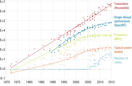
Nowadays, the computer industry, in order to cope with the various changes caused by technological and architectural advances, must take into account sev-eral key compromises. For decades, microprocessor architect designers have fo-cused on increasing the density of transistors within the single chip in order to increase their computational performance. The turning point was in 2005 when the limits of the law proposed by Robert H. Dennard came to light as shown in Figure 1.1. Dennard’s law is very related to that of Moore which is the number of transistors inside a chip, doubled almost every 18 months. Dennard claims that even the voltage necessary to power the chip could be properly scaled, in such a way as to make the power dissipated by the chip constant. Therefore, if every 18 months the number of transistors inside the chip doubled, it also doubled its characteristics of energy efficiency. However, Dennard did not take several factors into account:
• You can not set the voltage under a minimum threshold below which the chip does not work properly. The blocking of this scaling meant that the power dissipated by the chip was no longer constant and this led to the generation of a new problem called ”dark silicon”, an under-utilization of the transistors present inside the chip [25]. Since the maximum power dis-sipated by a chip with constant dimension is fixed, if the active transistors increase within it, this threshold will be overcome sooner or later, leading to chip breakage. The manufacturers then were forced to keep ”off” most of the transistors (sometimes even 60%) to avoid this problem;
Figure 1.1: Dennard Scaling.
• The phenomenon of leakage currents, which is the current that were gen-erated when the electrons, by tunnel effect, were able to overcome the insulating layer of CMOS transistors that, between the various production processes, became increasingly thinner. This phenomenon not only led to the increase of chip energy consumption, but also to the increase of its tem-perature and therefore, additional energy to dissipate excessive heat must be spent.
Thus, while Moore’s law continues to apply today, Dennard’s law came to a halt in 2005 when it faced an increase in performance per watt by a factor of only 1.2 rather than 2.8 expected. Hence the need to have to create new architectures, focus on parallelism and start thinking about energy efficiency as the true per-formance metric. This explains the shift to the multiple-core and the subsequent many-core ideas. The new architectures like FPGA, DSP and GPUs, introduced more challenging issues, then as now: interconnections, shared memory, coopera-tion, load balancing, dependency, synchronization and last but not least, ways for programmers to write applications that exploit the increasing number of proces-sors without loss in needed time or quality. Therefore, in contrast with the past, the reduction of the power consumption is currently a fundamental challenge and
it is becoming critical across all segments of computing, from the end-users who want ever longer battery life and lower weight and size for their laptops, tablets and smart-phones, to the data centres, whose power demands and cooling costs continue to rise.
1.2
High Performance Computing and
Heteroge-neous Systems
High Performance Computing (HPC) is a fundamental pillar of modern science. From predicting weather, to discovering new cancer treatments, to finding new energy sources, researchers use large computing systems to simulate and predict our world. Artificial Intelligence extends traditional HPC by allowing researchers to analyse large volumes of data for rapid insights where simulation alone cannot fully predict the real world. Data scientists are taking on increasingly complex challenges with Artificial Intelligence. From recognizing the speech to train vir-tual personal assistants in order to converse naturally to detect lanes on the road and obstacles in order to train self-driving cars. Solving these kinds of problems requires training exponentially more complex deep learning models in a practical amount of time. To deliver these new features, programmer productivity is an-other essential element to consider. It must be easy for software developers to tap into new capabilities by using powerful programming models in order to create new powerful algorithms and avoid to re-write legacy code for an ever expanding number of different platforms. Most of the applications demanding higher speeds at a bounded power consumption exhibit a high level of data parallelism. The key factor to achieve higher throughput and improve the power efficiency profile was the exploitation of massive data parallelism employing Graphics Processing Units (GPUs), Field Programmable Gate Array (FPGA) and Digital Signal Processors (DSPs). To fully exploit the capabilities of parallel execution units, it was essen-tial for computer system designers to think different. They re-architected com-puter systems to tightly integrate the disparate compute elements on a platform. Consequently all computing systems are gradually becoming heterogeneous, from mobile devices to supercomputers. Heterogeneous computing provides a coopera-tive paradigm leading to a separation of the application load in different portions. Serial and latency sensitive portion is handled by the CPUs and highly parallel one is demanded to a specific accelerator like the GPU which become ever more powerful and approach the general-purpose parallel computing world with a very interesting power efficiency profile Figure 1.2. This is why heterogeneous
com-Figure 1.2: Heterogeneous Systems Architecture
puting, which brings together the best of both CPUs, GPUs and DSPs worlds, is essential to get more powerful system with a better power efficiency profile. In the last few months we have also seen the emergence of heterogeneous sub-systems. Just think about the latest NVIDIA GPU architecture called Turing that includes CUDA Cores dedicated for floating point operations, Tensor Cores for AI acceleration and RT Cores for real-time ray tracing algorithms, all in a one chip.
As mentioned before, the rapid evolution of this context has not only impacted on the architectural choices, but has led to the need to create new programming models that take full advantage of the new hardware capabilities. ARM and In-tel has implemented new SIMD instruction set fore their microprocessors (NEON and AVX respectively) and NVIDIA with other manufacturer have introduced new programming models like CUDA, OpenCL and OpenACC. NVIDIA GPUs and the CUDA programming model employ an execution model called SIMT (Single Instruction, Multiple Thread). SIMT extends Flynn’s Taxonomy of com-puter architectures, which describes four classes of architectures in terms of their numbers of instruction and data streams. One of Flynn’s four classes, SIMD (Sin-gle Instruction, Multiple Data) is commonly used to describe architectures like GPUs. But there is a subtle but important difference between SIMD and SIMT. In a SIMD architecture, each instruction applies the same operation in parallel across many data elements. SIMD is typically implemented using processors with vector registers and execution units; a scalar thread issues vector instructions that execute in SIMD fashion. In a SIMT architecture, rather than a single thread is-suing vector instructions applied to data vectors, multiple threads issue common
instructions to arbitrary data. The benefits of SIMT for programmability led NVIDIA’s GPU architects to coin a new name for this architecture, rather than describing it as SIMD. NVIDIA GPUs execute warps of 32 parallel threads using SIMT, which enables each thread to access its own registers, to load and store from divergent addresses, and to follow divergent control flow paths. The CUDA compiler and the GPU work together to ensure the threads of a warp execute the same instruction sequences together as frequently as possible to maximize performance.
1.3
More Power is not enough!
In the just described context, the advance towards an always existed wall has passed almost noiselessly. The advent of heterogeneous and many-core computing exacerbates the gap between the processor and memory performance, the so called memory wall shown in Figure 1.3. Therefore, finding solutions to the memory wall is a crucial step to achieve the HPC target of human brain computing,
otherwise known as exascale computing. The memory performance does not
affect only the overall performance of the systems, but also impact on its energy performance. In particular, looking at today’s GPUs, the power contribution of data movement compared to processing can be as high as 85%.
This scenario presents new challenges for the memory infrastructure from the memory controller to the on-chip and off-chip design, the interconnection, caching, coherency etc. It is meaningful to underline that talking about memory performance can be misleading if not explicitly related to one of the two dimen-sions along which it extends: bandwidth and latency. The two concepts are not always directly related and a correct performance evaluation must be described along them to well understand pros and cons of new technologies. For instance, the newest technological innovation of 3D-stacked DRAM, benefits bandwidth-hungry HPC applications that show an high level of memory parallelism, but it is not expected to break the memory wall as claimed [66]. In this context, the on-chip memory has increased in importance and complexity along with the ad-vances in processor performance, to offload the larger but slower memories and to allow processing units to fastly communicate. This means that an efficient use of this precious resource would lead to lowered elapsed time for more complex al-gorithms employing them. These include scratch-pad memory in GPUs [85] (e.g. shared memory in NVIDIA devices), as well as dedicated on-chip memory banks in FPGAs, which can be possibly customized based on the application needs [16]. Such facilities are critical both for performance and energy consumption
Figure 1.3: The Unbreakable Memory Wall
[3] and are normally organized in a multi-banked structure, potentially enabling parallel data accesses to some regions of the address space. For these reasons, this work focuses its experimental phases on the on-chip scratch-pad memory pointing out some bottlenecks. In fact, when a resource is shared by multiple cores some problems could arise: the contention could generate conflicts and, a memory designed to give a high bandwidth serving multiple requests in parallel, could be accessed inefficiently, causing performance decreasing for the applica-tion. In addition, in some architecture like GPUs, the shared memory may be a limiting factor for the number of threads that can run concurrently, because of the inability to completely exploit the available resources.
Since the actual literature does not provide efficient solutions to efficiently reorganize conflictual access patterns, this work aims to mathematically describe the mapping problem and the related implications. Moreover, it presents some optimization techniques that, in some cases, do not involve extra memory and can decrease or eliminate multi-banked memory conflicts, in order to overcame the aforementioned problems and make the most of hardware performance.
1.4
Methodology
As mentioned before, this work aims to mathematically describe the memory mapping problem in order to determine some source code optimization that increase the system performance also in terms of performance per watt. This amounts to identify data layout transformations in order to:
Figure 1.4: The Polyhedral Approach
• decrease the communication and synchronization time between the various cores, and
• make the assignment of the different tasks to the various architectures of the system more efficient.
Contextualizing the research problem in the field of source code optimizations for GPUs, the first promising analytical model is certainly the polyhedral one which allows a very smooth and streamlined transformation of the data layout. The polyhedral model is a mathematical model that provides a powerful math-ematical abstraction to describe the possible transformations on grafted cycles, seeing each iteration as a whole point in a well-defined space called polyhedron. Thanks to this it is possible to use the linear algebra and linear programming tools to optimize the grafted cycles and to obtain improvements both on the location of the data and on the parallelization of the latter (see Figure 1.4).
Unfortunately, this model can only be applied to a certain category of data that represent a small percentage of those treated by the scientific community. In addition, some of the solutions obtained with this approach resulted in worsen-ing system performance as they wasted shared memory and thence limitworsen-ing the number of threads that can run concurrently on the GPUs.
So bearing that in mind, I started researching on which were the memory access patterns most used by the HPC applications. The result of this research is a pattern that I called Transpose Like. In this pattern, store operations are performed row-wise while load operations are performed column-wise, or vice
versa. Because of the finite number of banks in the local memory, different
store/load operations can incur conflicts. The approach used on this pattern aims at gaining a deeper understanding of conflict-avoiding techniques, resulting in a formulation of the problem that allows zero conflicts and zero memory overheads under most circumstances. In particular, the proposed methodology relies on
an Integer Linear Programming (ILP) model to describe the problem in terms of linear conditions ensuring optimal bank mapping strategies. I also propose a method for enumerating the solution space exhaustively and evaluating each solution based on the code complexity induced by the scheme.
The first Sections of the Chapters 3 and 4 briefly introduce the research context, the motivations, and the main objectives of each investigated research topic. Whereas, the corresponding last Sections are focused on the explanation of the methodology, the main scientific results and contribution of each Chapter.
Chapter 2
Technical Background
2.1
Introduction
The clock-frequency race, driven by Moore’s law, came to a sudden halt at around 2005. Since then, the semiconductor industry has settled on two main trajectories for designing microprocessor. The multi-core trajectory seeks to maintain the ex-ecution speed of sequential programs while moving into multiple cores. A current
exemplar is the recent Intel Core i7T M microprocessor, which has four
proces-sor cores, each of which is an out-of-order, multiple instruction issue procesproces-sor implementing the full x86 instruction-set, supporting hyper-threading with two hardware threads and is designed to maximize the execution speed of sequential programs. In contrast, the many-core(many-threads) trajectory focuses more on the execution throughput of parallel applications. An exemplar are the NVIDIA graphics processing units (GPUs) with more od 20.000 threads, executing in a large number of simple, in-order pipelines.
Many-core processors, especially the GPUs, have led the race of floating-point performance since 2005. As of 2012, the ratio between many-core GPUs and multi-core CPUs for peak floating-point calculation throughput is about 10 to 1 [48]. The motivations behind this trend are mainly related to the power consumption and the power dissipation that made the pursue of ever higher clock-frequency technologically and economically not sustainable. This is why many hardware vendors decided to move or start to produce massively multi-core chips, such as Tilera, Intel, Google etc. When designing and implementing a multi-core processor, there are different architectural challenges to consider. In fact, the multiple cores concept is not trivial, as it involves some challenges to be
addressed such as how the individual cores should communicate with each other and the outside world, and how the memory should be handled.
In the sections below are presented some technical knowledges on the new multi-, many-core architectures.
2.2
Memory and Data Movement
The design of a multiple-core architecture involves considerations about inter-core communication mechanisms. Historically [76] this problem has been addressed employing a common bus shared by all processors. The shared medium also fa-cilitated the implementation of cache coherency. But when the number of cores increases the bus solution begin to show its weaknesses because, even though it is cheap and easy to implement it does not scale very well. Latencies and bandwidth per core quickly becomes a critical issue. Newer and emerging mech-anisms such as multiple ring buses and switched on-chip networks are emerging and are becoming more and more common, due to lower power consumption, higher bandwidth or both [14, 15]. Continuing to increase the number of cores on a chip, the communication networks will face an ever increasing scalability problem and power-consumption constraints.
Memory interface is a crucial component of any high-performance processor and Multi-core processors are no exception. Modern high-end chips present the memory controller onto the chip and separated from the I/O-interfaces, to in-crease the memory bandwidth and to enable parallel access to both I/O devices and memory. Particular attention need to be paid to the Dynamic Random Access Memory (DRAM) controllers, because the development trend focuses on providing increased throughput rather than low latency. To leverage the so called row-locality, accesses are combined in such a way as to best utilize open pages and avoid unnecessary switching of DRAM pages so DRAM request schedulers do not maintain a FIFO ordering of requests from processors to the DRAM, in other words sequential consistency is not ensured. Some DRAM considerations related to an NVIDIA GPU DRAM controller are exposed later in Section 2.4.2. Within the context of many-core architectures, the memory infrastructure must be designed to better exploit the computational resources and hide long latencies due to off-chip memory accesses. In order to achieve this objective, modern architectures might have a new layer of communication between the processor cores, namely a shared memory, which can provide a way to interchange data at different speed levels. Shared memory can be on-chip or off-chip. In the first case, the shared memory is a kind of scratch-pad memory that can be used as
a user-managed data cache for data interchange, such as in NVIDIA GPUs. When shared memory resides on-chip, related traffic has a much higher bandwidth than off-chip memory. In the second case, for example, a slow big memory is shared among all the cores and its efficiency becomes a primary issue to argue about. Since the cores can use one or two levels of own cache memory, ensure that every core has always the exact same view of a shared location is a not trivial challenge. But this is not the only point to worry about, because specific stride access patterns can badly utilize the available memory, thus wasting bandwidth. More considerations related to an on-chip GPU scratch-pad memory are exposed in Section 2.4.2 Some multi- and many-core are distributed shared memory (DSM) systems implementing the illusion of a shared memory by using the message passing. These contexts provide many challenges to the hardware and compiler designers in order to obtain an abstraction of a common and consistent shared memory [62].
2.3
Hardware Multi-threading
Hardware multi-threading is a mechanism through which a core could support multiple thread contexts in hardware, so that multiple threads can share the resources of a single processor in an overlapping way in order to better utilize the available resources. To allow this mechanism, the processor must keep the state of each thread and be able to switch to another thread when, for example, one of them stalled because of high latency operations. The hardware context switch must be fast, it cannot require hundreds or thousands processor cycles as in process switch. The two main approaches to hardware multi-threading [36] are:
• Fine-grained multi-threading switches between threads on each instruction, resulting in interleaved execution of multiple threads. Each clock cycle any threads stalled are switched in favour of eligible threads. A disadvantage of this approach is that the single thread performance could be slowed down, since an eligible thread could not execute until another thread stalls. • Coarse-grained multi-threading switches threads only on costly stalls, such
as last-level cache misses. Unlike the fine-grained approach, this one much less likely slows down the execution of the single thread. But there is a disadvantage compared to the other approach in that it does not overcome throughput losses mainly due to shorter stalls.
A variation on hardware threading is provided by simultaneous multi-threading (SMT). This approach uses the resources of a multiple-issue processor to exploit thread-level parallelism. SMT processors often have more functional unit parallelism available than most single threads can effectively use. Without many changes to the processor architecture, SMT requires few main additions: the ability to fetch instructions from multiple threads per clock-cycle and a larger register file to hold data from multiple threads. Using register renaming and dy-namic scheduling multiple instructions from independent threads can be issued.
2.4
Modern architectures
This section provides a ten-thousand-foot view of the Intel Xeon PHI architec-tures, of the Graphics Processing Units and of the new Tensor Processing Units. Heterogeneous System on Chip (SoC) designs containing general purpose cores and domain-specific acceleration hardware are ever more employed to face the new challenges provided by the increasing demand of processing. They provide programmable computation for some portions of the application and hardware ac-celeration for specific-domain tasks. Treating specific portions of the application with hardware accelerators can provide significant speed-ups in specific-domain compared to software implementations. Moreover, they give a considerable bet-ter profile of the power consumption. This section focuses in greabet-ter details on Nvidia GPUs architecture as they have been extensively studied to present the performance implications of the problem showed in Section 2.4.2 and to evaluate the impact of the new mapping technique proposed in Chapter 3 and Chapter 4.
2.4.1
Intel Many Integrated Core (MIC)
The Intel Many Integrated Core Architecture is a many-core processor and co-processor based on the Intel Architecture. MIC architecture combines many Intel CPU cores into a single chip to address highly parallel workloads in HPC, machine learning, financial and engineering contexts. Knights Landing is the current, sec-ond generation (x200) of Xeon Phi coprocessors, the brand name used for all MIC architecture based products. This generation is available as either a processor or a coprocessor. The main reason that pushed Intel to extend Xeon Phi first gener-ation coprocessors to become processors is related to some limitgener-ations including limited memory size and PCIe transfers back and forth with a host processor. Basically Xeon Phi Knights Landing (hereinafter Knights Landing) is a proces-sor trapped into a co-procesproces-sor body [41]. Unlike GPUs, these products show
Figure 2.1: A Xeon Phi Processor.
Figure 2.2: Knight Landing ISA compared to the Xeon processors.
a greater flexibility in that they do not need to rely on particular programming models (like Nvidia CUDA) or subsets of standards like (such as OpenMP), as they supports all the features of C,C++, Fortran, OpenMP, etc. The following section describes the latest generation of Xeon Phi Knights Landing.
Knights Landing. Knights Landing is a many-core processor designed to deliver massive thread and data parallelism working on parallel workloads. It does not strictly need a host processor, as it can boot a stock operating system, thus getting rid of the limitations imposed by the PCIe data transfers. A Knights Landing product is manufactured in 14nm process and provide up to 72 cores. It introduces a new memory architecture providing two types of memory, MCDRAM and DDR and the new Advanced Vector Extensions 512 (AVX-512). The same code written for a Xeon Phi can also be compiled for standard Xeon processors. Figure 2.2 shows a comparison between the Xeon processors and Knights Landing ISAs.
Knights Landing architecture is based on the concept of tile. A basic overview is provided by Figure 2.3, where there are 38 tiles replicated, even if at most 36
Figure 2.3: Block diagram of Knights Landing processor architecture.
of them are active. Each tile is internally composed of two cores, two vector-processing units (VPUs) per core and a 1MB of L2 cache shared between the two cores, as shown in Figure 2.4. This means that each Knights Landing comprises up to 72 cores and 144 VPUs. Thanks to AVX instructions, the Knights Landing can explain all the potential of the VPUs. More details and considerations about AVX are presented in Section 2.6. Each core comes form an Intel Atom pro-cessor adapted to target the high performance computing. Some features were included such as support for four hyper-threads per core, higher L1 and L2 cache bandwidths, support for AVX-512, larger L1 cache etc. Nonetheless the new core supports all legacy x86 and x86-64 instructions. A Knight Landing core supports up to four hardware contexts using hyper-threading.
Inter-tile communication is possible thanks to a 2D-mesh interconnect, that also provides links to and from L2 caches other than that inside the tile, memory, PCIe. It is organized in such a way that traffic sent off the edge tile is folded upon the same tile. The mesh interconnect employs a MESIF cache-coherent protocol to keep all the L2 caches coherent. A distributed tag directory structure provides the tracking of the lines owned by each L1 and L2 cache. The caching/home agent (CHA) module of Figure 2.4 is demanded to hold and handle a portion of this distributed tag directory structure, as well as the channel through which the tile connects with the mesh. When a memory address is requested, the tile first query the local cache to know if data is available there. If not, it needs to query the CHA module of another tile. If the requested memory address is not cached,
Figure 2.4: Block diagram of a single tile.
the responsible tile will request it to the memory controller associated with that address. It’s clear that the developer should meet the needs of his application in the cleverest and efficient way. Knights Landing support the developer in getting more control on how cache data is handled, providing 3 different clustering modes: All-to-All, Quadrant/Hemisphere and sub-NUMA-4/sub-NUMA-2 (SNC-4/SNC-2). These modes are selectable from the BIOS at boot time. Below is presented a brief overview for each of the clustering modes.
• All-to-All: the default cluster mode where the whole memory address is uniformly distributed across all the CHAs.
• Quadrant/Hemisphere: the whole tiled-structure is subdivided into four quadrants or two hemispheres. The quadrant configuration guarantees that the memory addresses served by a memory controller are mapped only to CHAs of the quadrant it is associated with. The hemisphere mode operates in a similar way as it divides the tiled-structure in two hemispheres. • SNC-4/SNC-2: the whole tiled-structure is subdivided again into smaller
quadrants or hemispheres. Unlike the previous configurations, this one
exposes the quadrants or the hemispheres as NUMA nodes.
Note that, unless in quadrant/hemisphere mode each memory type is UMA, tech-nically the latencies vary across the mesh. However, in this case it is not possible to change the latency based on the choice of the memory location deterministi-cally. Therefore they need to be considered UMA. Using the SNC-2/SNC-4 mode the latency is lower when accessing near memory devices, that within the same
Figure 2.5: MCDRAM functioning modes.
quadrant, and higher when accessing memory of different quadrants. The authors of [41] describe the SNC-4 mode as well suited for MPI NUMA aware applica-tions that utilize four or a multiple of four ranks per Knights Landing. Exposing these features and providing the developer a way to change the configuration offer a greater flexibility in choosing the hardware configuration that better meet the application needs. On the other hand, the developer has to pay attention in choosing among the different configurations, as not all of them perfectly suit the application needs. Some of them could even decrease the performance. Knights Landing processor has two types of memory:
• Multi-Channel DRAM (MCDRAM): a high bandwidth, low capacity (up to 16GB) stacked DRAM comprising multiple channels vertically connected by means of through-silicon-vias (TSVs). All the channels can be accessed in parallel resulting in a higher throughput. Eight MCDRAM devices, each of 2 GB, are integrated on-package and controlled by a proper memory controller named EDC. This kind of memory introduces more flexibility from the developer point of view, as it provides three different functioning modes that can be selected at boot. It can be configured as a third level cache for DDR (cache mode), as a distinct NUMA memory (flat mode) or as an hybrid memory node (that is a combination of the two) as shown in Figure 2.5.
• DDR: resides outside of the Knights Landing package and offers high-capacity memory (up to 384GB). As shown in Figure 2.3, there are six memory channels controlled by two DDR4 memory controllers, one per side, so that each controller is associated with 3 channels.
Figure 2.3 also shows the presence of a PCIe block providing two x16 and one x4 lanes serving as masters. Some configurations of Knights Landing use the 2 x16 lanes to connect the Omni-Path Fabric resident on-package, thus leaving the x4 lanes for external devices and providing two Omni-Path ports out of the package.
2.4.2
GPU
Graphics Processing Units or GPU are specialized processors with hundred of parallel computing units used in combination with CPU to accelerate scientific, analytic, engineering and consumer applications. GPUs are currently employed in many energy-efficient datacenters, government labs, universities and small and medium business around the world and also in many other domains e.g. drones, robots and cars. Although the increasing diffusion, as already stated GPUs are not designed to replace CPUs. Therefore, an application developer can employ a heterogeneous execution model to implement massively parallel and compute intensive portions of an application, device code, on the GPU and serial portions, host code, on the CPU. An application executing on a heterogeneous platform is typically initialized by the CPU. With computational intensive applications, program sections often exhibit a rich amount of data parallelism. GPUs are used to accelerate the execution of this portion of data parallelism. NVIDIA is one of the leaders in GPUs supply in end-user and high performance computing markets. Its offer provides powerful solutions for visual computing and HPC and is now contributing to the deep-learning and automotive worlds with properly designed hardware such as:
• NVIDIA DGX-1 a deep learning supercomputer in a box;
• NVIDIA DRIVE PX series, combining deep learning, sensor fusion and surround vision to provide a complete autonomous driving platform. For these and many other reasons GPUs are significantly contributing to obtain better performance in many different domains and need to be described. The following section provides an overview of the NVIDIA GPU architecture deepen-ing some fundamental mechanism useful for the purposes of this thesis, namely everything related to the memory infrastructure.
Overview
NVIDIA provides several GPU models according to different architectural solu-tions. The large amount of GPGPUs provided by NVIDIA is commonly grouped on a compute capability basis. The compute capability of a device specifies its features and resources, e.g. the number of the so called CUDA cores per mul-tiprocessor, the number of special function unit, the amount of available shared memory and so on. A common heterogeneous system employing one or multiple GPUs has the aspect depicted in Figure 2.6. The PCIe link certainly provides less bandwidth compared to that used from both CPU and GPU to connect with
Figure 2.6: Link between CPU and one or more GPUs.
their own memory. The situation is compounded when using multiple GPUs with a PCIe switch.
GPU Processing Resources
In this section, the description of the resources follows the NVIDIA jargon and gives a feel of the scale of the available resources. A GPU compute device is char-acterized by a high number of CUDA corers. For example, the Pascal NVIDIA Titan X has 3584 CUDA cores, while a GTX 1080 has 2560 CUDA cores. Each of them has a pipelined 32 bit integer arithmetic logic unit (ALU) and floating point unit (FPU). The CUDA cores are grouped in Streaming Multiprocessors (SMs) (20 in a GTX 1080), each of which is able to execute blocks of threads. Each SM also comprises:
• Load/Store units to calculate source and destination addresses for the threads.
• Special Function Units (SFUs). Pipelined units used to execute transcen-dental instructions such as sin, cosine, square root etc.
gen-eration, for instance Maxwell architecture provides 4 warp schedulers per SM. It is basically an hardware unit used to issue instructions to the eligi-ble threads. A set of 32 threads is called warp. The warp scheduler plays an important role in a GPU architecture, as it is responsible to select the warps that have their data ready to process in order to hide the latency related to the memory accesses. Therefore, the more warps can be sched-uled, the more the memory latency can be hidden. But this concept will be extensively explained in the following sections.
• On-chip memory. Depending on the generation, the developer is able to par-tition it between L1 cache and scratch-pad memory, named shared memory in NVIDIA jargon. GTX 1080 provides 96 KB of shared memory and 48 KB of L1 cache storage.
• Register file. A chunk of memory used by the threads of the SM. There is zero wait time on this memory. It amounts to 256 KB for the GTX 1080. A GPU device consists of a certain number of SMs sharing a common off-chip memory area of L2 cache and a slower bigger off-chip memory named global memory. GTX1080 has 2048 KB of L2 cache and 8GB of GDDR5X RAM.
As stated few lines above, the warp scheduler represents an important block of the whole architecture. An important role is also played by the GigaThread Scheduler, that is a global scheduler that distributes thread blocks to the SM warp schedulers. The memory hierarchy will be deepened in the following section. GPU Memory Subsystem
One of the most important aspect of GPU performance is the memory subsystem. As stated in the first line of this section, the heterogeneous computing employing GPUs platform needs to execute massive parallel workloads, therefore, very high transfer rate to and from the memory system is needed. This leads to very strong requirements for the GPU memory subsystem, to supply which, the characteris-tics listed below are necessary:
• They need a very large number of pins to send data between the GPU and its memory devices. The memory system is organized such as a memory array comprising many DRAM chips to exploit the parallelism and provide a wide data bus width.
• They need to be fast. To maximize the data transfer rate, aggressive sig-nalling techniques are employed.
Figure 2.7: Example of partitioned memory.
• They try to use every available clock cycle to transfer data to or from memory array. Therefore, GPUs don’t care about latency, such as CPUs, rather they aim to maximize throughput and utilization efficiency.
• Compression techniques are used, both lossy and lossless, to convey as much data as possible.
• Hierarchical cache organization and work coalescing structures are used to reduce the effective off-chip memory traffic and to ensure high efficiency while transferring to and from memory array.
DRAM considerations
GPU design must take into account DRAM chips characteristics to achieve the enormous throughput requested by graphic and highly parallel computing appli-cations. Even if memory is perceived as a monolithic structure, DRAM chips are internally arranged as multiple banks, each of which comprises a power-of-2 number of rows and each row contains a power-of-2 number of bits. Several clock cycles are required to access a piece of data within a DRAM and the most part of them are needed to activate a row. But once a row is activated, the bits included in it are accessible with less clock cycles. GPUs have many different sources
Row Number Bank Channel Byte in a Page 32 21 20 17 16 13 12 0
Figure 2.8: DRAM addressing scheme.
of memory traffic, generating uncorrelated memory access requests, in contrast with the favourite access pattern for DRAMs. Therefore, the memory controller design is crucial to get better performance. A naive design solution could lead to the employment of different traffic queues for different banks. Each queue could wait for enough memory requests directed to an open row to join as much requests as possible in a single request to efficiently use the memory system, be-fore switching to a new row. Although this solution could increase row-locality, average latency related to each request will increase too. Therefore, the actual GPU design provides a partitioned memory, with each partition controlled by an independent memory controller and one or more DRAM devices as shown in Figure 2.7. A practical example of this architecture can be deepened in patent in patent [77]. This scenario also needs a way to interleave addresses among the partitions to achieve theoretical N × one − partition performance. The chosen interleaving can benefit or harm the bandwidth of some applications, therefore the choice of the stride between two consecutive partitions became crucial. It typically amounts to few hundred of bytes as also stated in patent [24]. Memory subsystem does not ensure sequential consistency. The order of memory read or write to the same address in a thread program is preserved, but the order of accesses to different addresses may not be preserved. The DRAM world opens some other issues related to the protection besides the performance. In fact, the knowledge of the aforementioned features is also important when thinking about the mapping scheme from the physical address space to the specific DRAM lo-cation. To explain in more details how a mapping could have place and to give a dimension to the considerations suppose a physical addressing space of 4GB (32-bit) as example. A possible address mapping of physical address to DRAM is depicted in Figure 2.8.
• Bits 12-0 identify a byte within a 8KB page (213 = 8192byte = 8KB); • Bits 16-13 identify which one of the 16 memory channels the system will
use for this address;
• Bits 20-17 identify which one of the 16 banks has to be accessed to get the data.
Figure 2.9: Minimalist Open-Page and the permutation-based page interleaving schemes.
• Bits 32-21 identify which row within a bank has to be accessed.
The bits within the channel field serve to subdivide the banks among the DRAM modules in order to increase the bandwidth. The channel field is placed there with a clever purpose: it allows the spread of sequential accesses on different channels thus increasing the parallelism. In some cases a channel hashing has been employed. This is the case of Ivy Bridge architectures, where the channel selection is based on multiple address bits[40], in order to allow a more even
distribution of memory accesses across channels. A memory bank can serve
one request at a time. Any other access directed to the same bank need to wait until the previous access has been completed, thus causing a bank conflict. Conversely, accesses directed to different banks can proceed in parallel, for this reason the bank number change earlier than the row number, as the address increases. Generally the bank, column and row numbers are properly organized to minimize the so called bank thrashing, namely a continuous change of a specific
row in a bank. This is a fundamental question, as bank trashing can cause
significant problems, such as the row hammering problem, that is the repeated activation of two rows. It can lead the memory cells to leak their charge and altering the content of nearby memory rows.
mechanism employed before the physical address-DRAM mapping) could cause many serious troubles in economic and healthy way. The row-hammer bug be-longs to the Zero-day vulnerabilities and has been studied by the Zero-Project
of Google in [70] and [46]. A zero-day vulnerability is basically known as a
”zero-day” because it is not publicly reported or announced before becoming ac-tive, preventing the software’s author to create patches or advise workarounds to mitigate against its actions. The literature provides different address mapping schemes such as the Minimalist Open-Page scheme [44] and the Permutation-based page interleaving scheme depicted in Figure 2.9. Suppose a large vector accessed each time at a relatively high distance from the previous one. In this case a solution to prevent bank thrashing is to XOR the lower part of the row number with the bank number. With the previous mapping scheme the address X and X + 256K would fall in the same bank but at different rows. This situation could be avoided XORing parts of the starting address. From the afore described considerations results that it is important to know how to handle similar prob-lems in GPUs and in general, in many-core/heterogeneous systems, where the memory wall is still up.
The row-hammer bug is indicative of a dependence on the access pattern. This means that the latter could also provide better or worse performance depending on the couple (mapping-scheme, access-pattern), because a fixed access pattern can better exploit the bandwidth than another. But the main problem is that the context of general-purpose computing provides many different applications, each with its own access pattern. What would benefit the application performance is to have the chance to always select a good couple. However this kind of solution raises new issues such as:
• if the access pattern changes during the execution how the mapping could be changed to face the new pattern?
• how is possible to detect a change in the access pattern?
• if a feasible and efficient solution can change the access pattern how the previously placed date would be affected? It would require a data migra-tion?
A dissection of the main problem and of the related issues is reported in [32], where the access pattern detection is executed with an array of counters tracking the change rate of each bit of the requested address and generating a new mapping scheme based on it. When it comes to the change of the access pattern during the execution of a specific application, the authors propose a data migration solution
Figure 2.10: NVIDIA Tesla P100.
and a reboot-based solution. The first involving the migration of all the previously placed data, thus involving some kind of a mechanism to track the dirtiness of a location, The second based on the reboot to change the mapping scheme and replace data. Given the heterogeneous nature of the wide range of applications access pattern, none of the proposed solution can be a priori discarded. The same data migration problem raises when coming to problems related to the power consumption of the memory infrastructure. As patented by Apple in [35] the memory address space can be partitioned across different memory mapping functions. The memory controller may use a first memory mapping function when a first number of memory banks is active and a second memory mapping function when a second number is active. When one of the memory banks is to be deactivated, the memory controller may copy data from only the memory bank that is to be deactivated to the active remainder of memory banks.
From a technological point of view modern GPUs rely on Graphics Double Data Rate (GDDR) to achieve a high bandwidth. As the DDR main memory standards, GDDR memory device standards are set by the Joint Electron De-vice Engineering Council (JEDEC). The most recent generation of the GDDR standard is GDDR5X. JEDEC specifies 512Mb, 1Gb, 2Gb, 4Gb, 8Gb and 16Gb densities [19]. Unlike DDR memory devices, GDDRs support wide bus up to 512bit. GDDR5X generation is characterized by a 8n pre-fetching architecture. This means that a single write or read access is burst oriented: an access starting at a selected 4-byte location on a 32-bit wide link consists of a 256bit long data transfer corresponding to a total of eight 32bit data words. With the introduction
of the 3D stacked memory, also the GPU design can benefit of a higher band-width. Consequently, NVIDIA started to embed these kind of memories within the newest platforms, such as in Tesla P100 [63], shown in Figure 2.10.
NVIDIA GPU Memory System
As already stated in the previous sections, NVIDIA GPU memory subsystem is structured in a hierarchical way. Each one of the different types of memory of the GPU has a specific use, limitations and performance profile. A typical heterogeneous application is composed of a section of code through which data to be processed is first transferred from the host memory to the device memory. Then, the threads can access their portion of data on a thread ID and/or block ID basis. This memory is called global memory and is typically implemented with off-chip dynamic random access memory (DRAM), which tends to have a very long access time as well as a low access bandwidth (hundred of clock cycles). Since many workloads need very high load and store operation latencies, a faster and high-bandwidth memory could improve the application performance. But, as it is well known, it can cost too much to have low-latency memories. So, with a well designed memory model data can be properly placed to get optimal performance. The design of a memory model often relies on the concepts of locality. Indeed, a common application does not access always arbitrary data. Instead, they often satisfy the principle of spatial or temporal locality, respectively space related and time related locality. The memory hierarchy is based on the aforementioned principles. Therefore, different levels of the hierarchy provide different latencies, bandwidth and capacities in order to abstract a large and low-latency memory. The memory model exposed by CUDA is characterized by the following kind of memories: • Registers; • Cache L1/L2; • Shared memory; • Local memory; • Constant memory; • Texture memory; • Global memory.
From them, the L1 and L2 caches are the only not programmable memo-ries.
Registers
Registers are the fastest level of the memory hierarchy. Typically the au-tomatic variable of a kernel without no other qualifier is stored in a register. Registers are allocated per thread, so the variables are private to each thread. But they are shared among all the threads, so there is an hardware limit to the number of registers available per thread. For instance a Kepler architecture pro-vides up to 255 registers per thread. The limit does not prevent an application to use more threads, the key is to spill over to local memory the excess regis-ters, precisely with a register spilling operation. In order to have low-latencies for as much accesses as possible, the frequently accessed variables are placed in registers.
Local memory
All the variables that do not fit in the registers area can be allocated into a local memory. So this memory space also holds the spilled registers. Although the name might suggest such a private and fast memory, the local memory area resides in the same physical location as global memory. In terms of elapsed time to load or store from/in a local memory location it means a high latency and low bandwidth access. The local memory is typically managed by the compiler which decides to place data there when belonging to large local structure or when even if not so large, the arrays can not be indexed with values known at compile-time.
Shared memory
Shared memory is local to each cooperative thread array (CTA) or thread block and only visible to the threads within it. Its lifetime coincides with the CTA lifetime, i.e. it is created together with the CTA and destroyed when it terminates. To place variables in shared memory they need to be accompanied by the shared attribute. Shared memory resides on-chip, therefore, related traffic has a much higher bandwidth than off-chip global memory. It can be thought as on-chip scratch-pad memory that can be used as a user-managed data cache or as a mechanism for fast data interchange between threads of the same CTA, that could also enable memory coalescing. To achieve high memory bandwidth for concurrent accesses, shared memory is divided into equally sized banks simul-taneously accessible. A memory load/store access of n addresses that covers k distinct banks can proceed with a higher bandwidth, k times higher than a single bank bandwidth. A memory access request of n addresses mapped to the same
memory bank, leads to bank conflicts and the memory accesses will be serialized, because the hardware splits a conflicting memory request into separate conflict-free requests. When this scenario occurs the effective bandwidth unavoidably decreases. Moreover, when all threads of a warp, request the same address, all memory accesses will address the same bank, but this case results in a broad-cast rather than a serialization. To increase effective bandwidth and minimize bank conflicts, it is important to know how shared memory addresses map to memory banks. If each bank is 32bit wide, successive 32bit words will map to successive banks. NVIDIA Kepler architecture has introduced a double mapping scheme for shared memory. Indeed, the application developer has the ability to configure it to work in four-bytes or eight-bytes mode as will be better covered in Section 2.4.2. Another degree of freedom for application developer is brought by the partitioning size of shared memory against L1 cache. On device of compute capability 2.x and 3.x the available on-chip memory can be partitioned between L1 cache and shared memory. For devices of compute capability 2.x two avail-able settings split the 64KB on-chip memory as 48KB shared memory / 16KB L1 cache or 16KB shared memory / 48KB L1 cache. Newer architecture, like Maxwell removed this degree of freedom increasing the available shared mem-ory size. Each SM has a fixed amount of shared-memmem-ory that will be subdivided among all the thread blocks. Therefore, if each thread block uses too much of this resource the number of simultaneously active warps can decrease, thus causing degraded performance. This scenario represents a limiting factor shared memory condition. The course of this thesis will explain some instances of this scenario, pointing out the possible solutions.
Global memory
Global memory resides off-chip in device memory and is the largest and slow-est of the hierarchy. Any thread of any SM can access the global memory, as it has a global scope and lifetime. Concurrent accesses to global memory from mul-tiple threads are not automatically synchronized to avoid them to concurrently modify the same location, so it needs to be carefully managed. As already stated global memory resides off-chip, namely it refers to an external DRAM memory space which is not local to any one of the physical SMs. Global memory is ac-cessed via 32byte, 64byte or 128bytes transactions. When the threads of a warp execute an instruction that accesses global memory, the hardware can coalesce the memory accesses in one or more transactions analysing the size of the word accessed by each thread and the distribution of the memory addresses related to each request (More details in Section 2.4.2). Suppose a 32-words memory access
Figure 2.11: Memory model exposed by CUDA.
request arrives with each word of 4 bytes, if the addresses are naturally aligned and sequentially arranged the hardware will coalesce the whole 128byte-access request in a single transaction. If the addresses are arranged in a 128byte stride pattern, the hardware will generate 32 memory transactions of 128bytes each, to satisfy the initial request. This way will lead to a decreased bandwidth by a factor of 32 because all the words but the one effectively requested, represent wasted bandwidth.
The analysis and optimization of the global memory access pattern is crucial to reach better exploitation of the available bandwidth and to prevent SMs to wait while the memory request are served. Even if the number of simultaneously executing threads is very high, global memory long latencies are not always tol-erable. In fact, an application could exhibit a traffic congestion in the global memory access paths that prevents all but few threads from execute, leaving some or most of the streaming multiprocessors idle. This scenario points out the importance of having an efficient access pattern to the global memory to get better performance.
Caches
As shown in Figure 2.11 the L1 caches are local to each SM. While the L2 cache is shared among all SMs. The whole L2 cache is split in hierarchy is depicted in different slices of L2 cache. Both L1 and L2 caches are used in combination with local and global memory accesses, including register spills. On devices of compute capability 2.x and 3.x, local memory and global memory accesses are always cached in L1 and L2. Instead, on devices of compute capability 5.x, local memory and global memory accesses are always cached in L2. However, this memory model provides that only memory load can be cached, while memory
store operations cannot be cached. As stated in [52], the cache replacement
policy does not follow a Last Recently Used (LRU) rule and properly written micro-benchmarks can give the specific cache replacement policy. Each SM also offers a read-only constant cache and a read-only texture cache used to hide the latency of accessing a device memory space, thus improving the performance experienced in read operations. In Figure 2.12 is shown the memory architecture of a NVIDIA GTX 970. There are 4 memory partitions each comprising two DRAM memory controllers (MC) and two slices of L2 cache. The whole L2 cache space is shared among all the SMs through a crossbar interconnection to allow any SM to connect to any L2 cache slice. The obscured SMs and L2 slice belong to the floor sweeping technique, used to produce functionally acceptable processing units (GPU o CPU o DSP), that would otherwise be production waste, because of some sort of manufacturing faults. When the essential functionalities are not impacted the processing unit can be salvaged and used as totally functioning unit, although with reduced functionalities or capabilities. A manufacturing faults could occur in partition circuitry. This means that the presence of multiple partitions gives the opportunity to save some otherwise manufacturing waste, compared to a single bigger partition. This flexibility provides more work and complexity to the memory management unit (MMU), which must be able to withstand and handle a manufacturing fault [24].
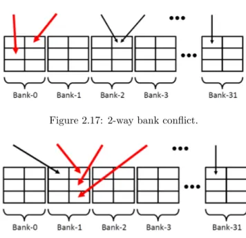
Shared Memory Bank Conflicts Considerations
As mentioned before, mainly for performance purpose, shared memory is divided in banks, which can be accessed in a parallel way from all the threads in a warp.
The number of banks is strictly dependent from the architecture. In Kepler
architecture, and only in this architecture, the number of banks is 32 and each bank have a word of 8 bytes. In the other architecture, each bank have a word of 4 byte and data are cyclically distributed over the bank only with 4-byte access shown below. Data allocated in the shared memory are cyclically distributed over the banks in two ways:
Figure 2.12: GTX 970 memory architecture.
• 4-byte access : Successive 4-byte words go to successive banks. We must think that we have 32 banks, 4-byte wide. If the data that we use is 8 bytes wide, the access mode became the 8-byte access.
• 8-byte access: : Successive 8-byte words go to successive banks. We can compute easily in which bank a data is stored in this way:
– (8 B word index) mod 32; – (4 B word index) mod 32 ∗ 2; – ((byte address) mod 32 ∗ 8.
The Figure 2.13 shows an example of data mapping on shared memory with both modalities. In this example the data are 4B-word index and, for simplicity, we use only for 4 banks.
The access mode can affect the performance of the kernel. Sometimes an access-mode, rather than the other, can avoid a critical problem like the bank access conflict discussed below.
Allowing all the threads in a warp to fetch data in parallel from this kind of memory can lead to great performance improvements, but is not quite easy to extract high throughput without managing it carefully and in an explicit way.
There are three main working modalities for the shared memory which guar-antee great performances: