Università Politecnica delle Marche
Scuola di Dottorato di Ricerca in Scienze dell’Ingegneria
Curriculum in Ingegneria Biomedica, Elettronica e delle Telecomunicazioni ---
Technologies for the Integration of
Waveguide Components and Antennas on
Printed Circuit Boards
Ph.D. Dissertation of:
Francesco Bigelli
Advisor:
Prof. Marco Farina Curriculum supervisor:
Prof. Franco Chiaraluce
Università Politecnica delle Marche
Scuola di Dottorato di Ricerca in Scienze dell’Ingegneria Curriculum in Ingegneria Biomedica, Elettronica e delle Telecomunicazioni
---
Technologies for the Integration of
Waveguide Components and Antennas on
Printed Circuit Boards
Ph.D. Dissertation of:
Francesco Bigelli
Advisor:
Prof. Marco Farina Curriculum supervisor:
Prof. Franco Chiaraluce
Università Politecnica delle Marche
Dipartimento di Ingegneria dell’Informazione
Abstract
In this research work I present the feasibility study on the realization of a class of devices in SIW (Substrate Integrated Waveguide) technology for ICT application at microwave frequencies. With this technology it is possible to obtain, by the traditional processes for the printed circuits manufacturing, integrated components with quality factors greater than the microstrip and the stripline.
SIW technology is very promising because it permits to obtain compact, low cost and self-shielding guiding structures and hence, guides components. Although many papers, presented in literature, strengthen these qualities, this technology did not lead to an industrial production today, even at low volumes.
This work is part of the formation project annexed to its research project, entitled “Integrated Waveguide (SIW) technologies development for microwave ICT applications” in collaboration with the Politecnico of Bari, Università Politecnica delle Marche and SOMACIS SpA, a worldwide PCB (Printed Circuit Board) industry with forty years of experience in the highly technological sector of high-mix and low-volume.
As this hopeful technology allows a drastic reduction in size and costs, qualities that are well suited to the increasing market needs, the project aims to design and realize a class of product ranging from filter, hybrids, “frequency-shaping” components and antenna. SIW technology could also permit to produce in a large scale expensive and complicated products like the automotive and defense radars. Moreover, in the market of civil telecommunication, it could be possible to replace the standard and bulky TV dishes with planar array of antenna that are more competitive and could have a wide spread. Such array could also be fully integrated in the roof like it happens for the solar panels, this advantage could drive people to opt for these new concept of satellite antennas. Indeed, it seems to be realistic to foresee a market of thousands of components overlooking the proper motivation to the success of the project.
The SIW technology permits to reproduce in a planar form, through rows of metallic holes, a traditional waveguide. Obviously, in these structures, the electromagnetic field travels into the dielectric and not in air. It is clear that this involves a sensible increase of the losses. Even if the dielectric losses are the dominant part, these are still enhanced from a high density of current localized in the metallic holes that constitute the lateral sidewalls.
In recent years several Substrate Integrated Waveguide devices such as antennas [1-2], filters, and couplers [3-4, 5-6] have been reported in literature. SIW technology is a good technique for designing and fabricating microwave and millimeter-wave devices and circuits [7-21]. However, an industrial use of SIW components still requires an essential phase of systematic study.
Therefore the first objective of this study consists in optimization of technologies most suitable for the realization of this components.
Contents
1. Introduction 01
1.1 Substrate Integrated Waveguide (SIW) technology 01
2. Material characterization 05
2.1 Physical characteristics of materials for Printed Circuits 05
2.1.1 Glass transition temperature 05
2.1.1.1 Thermal expansion 06
2.1.1.2 Degree of cure 07
2.2 Dielectric constant measurements 08
2.2.1 Narrow band measurement methods 09
2.2.1.1 IPC TM-650 2.5.5.5c 09
2.2.1.2 Split cylinder resonator 11
2.2.1.3 SIW resonator 13
2.2.2 Broadband measurement methods 15
2.2.2.1 Partially loaded waveguide 15 2.2.2.2 Differential phase length 18
2.3 Non-ideal effects of laminate structure 21
2.3.1 Power loss due to periodic texture 22 2.3.2 Signal integrity effects of fiber weave 24 2.3.3 SIW texture dependency investigation 24
2.4 Material selection criteria 28
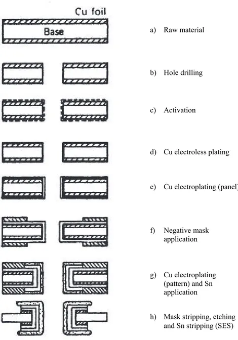
3. PCB PTFE-based manufacturing process 32
3.1 Semi-additive process 32
3.1.1 Mechanical drilling 34
3.1.2 Desmear, electroless and electrolytic panel plating 39
3.1.3 Imaging 41
3.1.4 Electrolytic pattern plating 43
4. Prototype design and development 47
4.1 SMA to SIW transitions 47
4.1.1 Two ports transition 47
4.1.2 Three ports transition 49
4.2 Transmission line 50
4.3 Power Divider 51
4.4 Directional Couplers 55
4.4.1 Four ports coupler 55
4.4.2 Six ports coupler 58
4.5 Antenna 62
4.5.1 Elementary radiators 63
4.5.2 Feed line 69
4.5.3 Radiating blocks and external region 74
4.5.4 Experimental characterization 76
4.5.4.1 Return loss 77
4.5.4.2 Radiation pattern 78
4.5.4.3 Gain 80
5. Fabrication process for losses reduction 81
5.1 Planar hollow waveguide: the state of art 82
5.2 Dielectricless SIW 85
5.2.1 Fabrication methodology 85
5.2.2 Performances 91
5.2.3 Slotted antenna design 93
5.3 Hybrid antenna development 96
6. Concluding Remarks
6.1 Conclusions 98
List of Figures
Fig. 1.1: a) Traditional hollow Rectangular Waveguide (RWG) b) Dielectric Filled Waveguide (DFW)
c) Substrate Integrated Waveguide (SIW) 02
Fig. 1.2: Equivalence between a SIW and a DFW 03
Fig. 1.3: Geometry of the vias, here are evidenced the diameter (d) and the pitch (p) 03 Fig. 2.1: Expansion of a resin-based material vs. temperature 06
Fig. 2.2: Measuring resonant frequency and Q 09
Fig. 2.3: Generalized resonator pattern card matching the nominal permittivity of
material to be tested, all the quotes in millimeters 10
Fig. 2.4: Split cylinder resonator – experimental setup 12 Fig. 2.5: SIW resonator – CAD model on the left and the prototype on the right 13 Fig. 2.6: SIW resonator frequency response – experimental vs. simulated results 14 Fig. 2.7: Schematic representation of the measurement setup on the left and circuital
representation on the right 15
Fig. 2.8: Specimens of RF-35A2 and the waveguide WR90 17
Fig. 2.9: Average of three samples of Taconic RF35-A2, Dk on the left and Df on the right 18
Fig. 2.10: Two segments of line in SIW technology with different lengths 19 Fig. 2.11: Dielectric constant measured with the Differential Phase Length Method.
The solid line is the permittivity calculated, the dashed line is the nominal value 20 Fig. 2.12: Fiberglass cloth: a) 106, b)1080, c) 2113, d) 2116, e) 1652, f) 7628 21 Fig. 2.13: Mono-dimensional representation of a laminate 22 Fig. 2.14: Simulated and theoretical Brillouin zones. a) Insertion loss profiles of 60, 45, 30
and 15 mil period. b) theoretical evanescent zones of the 60 mil period. Courtesy of [25] 23 Fig. 2.15: Cross-section of two microstrips: one runs on the glass and the other one on the resin 24 Fig. 2.16: Cross-section of a thought hole on a laminate of Taconic RF-35A2. It is
noticeable the inhomogeneous structure of the material: in black the bundles and in
Fig. 2.17: Panel of Taconic RF-35A2 with couple of lines with different orientation respect the bundle. Below, a detail of line disposed with a tilt of 40°. Thanks to the
bright material the bundles externally (dark and parallel stripes) are visible 26 Fig. 2.18: Trend of the dielectric constant over frequency and over the tilt angle at
the frequency of mid-band for the Taconic RF-35A2 in the DVB-S band. The
black dashed lines represent the nominal value 27
Fig. 3.1: Key manufacturing steps in pattern plating method. In detail the electroplating of
a through hole with relative pads. Courtesy of [27] 33
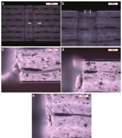
Fig. 3.2: Preliminary drilling test: a) microsection of the hole, b) c) d) e) details of
residuals in its interior 35
Fig. 3.3: The “Daisy chain” scheme. In detail the single cell formed of tracks on the top
layer in red, tracks on the bottom layer in green and holes connecting all of them in yellow 36 Fig. 3.4: First Daisy chain test on a laminate of Taconic RF-35A2 machined with standard parameters. In detail the withdrawal of the sample analyzed 37 Fig. 3.5: Microsection of opens detected with the Daisy chain test. The red arrows indicate the points of misconnection between the copper foil and the copper deposited inside the holes 38
Fig. 3.6: Detail of skip plating 38
Fig. 3.7: Microsection after the metallization stage. The original laminate copper is 17 µm, reduced down to 14.6 µm after the micro-etching. Each metallization step (2 in total) brings around 6 µm of copper inside the holes and on the panel surface for a total of 12 µm. It can be observed the transition between the laminate and the hole copper, where in a localized area only 5.6 µm are deposited: it would be a copper void in absence of the second metallization step 40 Fig. 3.8: Surface structure after processing with Aluminum Oxide cleaning 41
Fig. 3.9: Basic scheme of a typical electrolytic cell 43
Fig. 3.10: Microsection of a hole after the electrolytic line. Inside the holes the deposit
of copper is around 37 µm, while on the external surface copper thickness is almost 50 µm 44 Fig. 3.11: Pattern shrinkage due to the lateral etching. The yellow arrows represent the etching direction, while the blue boxes represent the tin (etch-resist) 45 Fig. 4.1: Sketch of the transition, a 45° view on the left and a top view on the right 48 Fig. 4.2: Reflection coefficients of a 2 port transition SMA-SIW. Red and blue line are
relative to the SIW and coaxial port respectively 49
Fig. 4.3: Reflection coefficients of a 3 port transition SMA-SIW. Red and green lines are
relative to the coaxial and SIWs (equal for symmetry) ports respectively 49 Fig. 4.4: A segment long 109 mm of a SIW transmission line. At the end of the guide are
Fig. 4.5: Comparison between simulation and measurement of a segment of SIW in
Taconic RF-35A2 long 109 mm 51
Fig. 4.6: A balanced power divider in SIW technology: A) septum; B) iris; C) λ/4 adapter 52
Fig. 4.7: Prototype of a 3dB power divider 53
Fig. 4.8: Simulated and measured reflection coefficients 53 Fig. 4.9: Simulated and measured transmission coefficients 54 Fig. 4.10: Conceptual design of the directional coupler with the numbering of the ports 55 Fig. 4.11: Degrees of freedom of the directional coupler proposed 56
Fig. 4.12: Prototype of a 3dB directional coupler 57
Fig. 4.13: Experimental S-parameters of the 4 ports directional coupler 57 Fig. 4.14: Difference of phase between the direct and the coupled ports 58 Fig. 4.15: Three different schemes for the six ports directional coupler 59 Fig. 4.16: The six ports directional coupler structure with the numbering of the ports and
the two plane of symmetry (dash lines) 60
Fig. 4.17: Six ports directional coupler in SIW technology with the transitions for the connectors 61 Fig. 4.18: S-parameters related to the port 1 (a) and to the port 2 (b) 61 Fig. 4.19: Surface current of a waveguide with the TE10 mode in propagation 63
Fig. 4.20: Basic scheme with elementary radiators (2x2) composed by displaced slots where are highlighted with the letters:
I for the input port; P for the power dividers;
S for the slots 64
Fig. 4.21: 3D plot of the total gain of the 2x2 elementary radiators with single slot at the lower,
middle and higher frequencies of the band 65
Fig. 4.22: a) Modified basic scheme with elementary radiators composed by the paired slots (in yellow) and the metallized via (in red); b) Boresight of the modified scheme at the lower,
middle and higher frequencies of the band 66
Fig. 4.23: Top view of the first array prototype. Are marked the following relevant parts: C) hole for the coaxial connector;
M) matching stage for the connector; P) power dividers;
S) pair of slots;
Fig. 4.24: Simulated (blue-dashed) and measured (green-solid) |S11| 67
Fig. 4.25: Simulated (blue-dashed) and measured (green-solid) at 11 GHz H-plane radiation pattern (on the left) and E-plane radiation pattern (on the right) 68
Fig. 4.26: Sketch of the corporate feed network 69
Fig. 4.27: Three port power divider on the left and the relative frequency response on the right 70 Fig. 4.28: (a) The first two blocks of the feed line: the coaxial transition and a power
divider. (b) Reflection coefficient of the composition of the first two blocks seen at the
coaxial port 71
Fig. 4.29: (a) Five relevant blocks constituting the feed line. (b) Overall reflection
coefficient of the composition 72
Fig. 4.30: Comparison between simulated S11 (a) and S12 (b) of the BFN. In green the
real dielectric with Df = 0 and in blue the ideal dielectric with Df = 0 73 Fig. 4.31: Composition of the internal and external region through the blocks containing
the slots, represented by the admittance matrixes; th is the thickness of the copper where are etched the slots and M is the number of the accessible modes per slot 74 Fig. 4.32: CAM representation of the composition of feed line and the elementary radiators. In the middle of the structure is placed the coaxial transition 76 Fig. 4.33: First prototype of the SIW antenna, with dimensions of 352x352 mm, realized over
a substrate of Taconic RF-35A2 77
Fig. 4.34: Reflection coefficient in the band 10.7 – 12.7 GHz. Simulation (blue dashed)
and measurement (green solid). The blue marker defines the rage of variability of tanδ 77 Fig. 4.35: Radiation pattern in the E-plane (blue solid) and in the H-plane (green solid) of
the planar array at the frequency of mid-band 11.7 GHz 78
Fig. 4.36: Shift of the main lobe in the E-plane measured at the middle and peripheral frequencies 79 Fig. 4.37: Shift of the main lobe in the H-plane measured at the middle and peripheral frequencies 79 Fig. 4.38: Simulated (solid line) and measured (dashed line) gain vs frequency 80 Fig. 5.1: Concept design of a PSIW on the left and detail of middle part of the PSIW on the right. The grey part are the dielectric hosting the metallized vias, the yellow parts are the
top and bottom covers (Courtesy of [40]) 82
Fig. 5.2: Example of a 3-port directional coupler in PSIW. (a) Three layers of PSIW without the top and bottom covers, (b) top and (c) bottom view of the components so realized.
(Courtesy of [40]) 83
Fig. 5.4: Half-processed HSIW with the detail of the vias plugging on the left and the
structure at the final stage on the right. (Courtesy of [41]) 84 Fig. 5.5: Milled base material laminate. In foreground, the transition for the SMA connector 86 Fig. 5.6: Panel after the metallization process. It appears completely covered with copper 87
Fig. 5.7: Laser scoring of sheet of no-flow prepreg 88
Fig. 5.8: Top view of the mass-lam. Three scored sheets of Kraft paper ensure the perfect
rectangular geometry of the guide 88
Fig. 5.9: Resulting mass lamination composed by the milled guide (yellow part on the bottom), the prepreg (red sheet) and the cover (yellow part on the top). On the right, the detail of the oversizing of the aperture over the prepreg before the lamination process. Thickness not in scale 89 Fig. 5.10: Sketch of the section of the waveguide. The green part is the dielectric, the red part is the prepreg and the yellow parts are the metallized faces. Electrical continuity is enforced by vias (orange vertical cylinder) around the waveguide. Thickness not in scale 90 Fig. 5.11: Metallographic cross-section of the guide. The copper thickness is reported in each layer and verified the low expansion of the no-flow prepreg. It is noticeable the slight resin
flow inside the guide 90
Fig. 5.12: Simulated propagation constant of the Dielectricless SIW (dashed line) and corresponding traditional waveguide (solid line), its inner dimensions are a = 16 mm and
b = 1.52 mm 91
Fig. 5.13: Comparative simulation between real part of the propagation constant of waveguides filled with different materials and the proposed structure 92 Fig. 5.14: CAD model of the designed antenna. The green box constitutes the interior part of the guide and the slots are represented on the top in yellow. It has been simulated also the SMA connector and the radiation box enclosing the structure. In detail, the cross-section of the guide in correspondence of the coaxial transition, where the purple cylinder represent the Teflon of the SMA connector and inside of it the central conductor that penetrates the
Dielectric-Less waveguide 94
Fig. 5.15: First prototype of a dielectric-less slotted antenna. It is noticeable the series of plated through holes around the guide and the hole in the middle for the coaxial connector 94
Fig. 5.16: Reflection coefficient S11 of the input port 95
Fig. 5.17: Azimuth radiation pattern. Here, to maintain the diagram compact, simulated values inferior to -25dB were ignored because are smaller than the sensitivity to the measuring system 95 Fig. 5.18: Bottom view of the Hybrid antenna concept. On the light green laminate in
background are derived the SIW radiators. The blue draw is the corporate feed line in
Fig. 5.19: Top-diagonal view of the Hybrid antenna. In detail the transition between the feed
Chapter 1.
Introduction
1.1. Substrate Integrated Waveguide (SIW) technology
In high frequency applications, the microstrip, that is the most popular technology on the printed circuits, is not efficient when the wavelength becomes small; therefore, the manufacturing of such devices requires tolerances on the production process more and more limited.
Vice versa, at high frequencies (above the GHz), the waveguides are preferred, thanks to their low losses and to the high power handling. Conversely, waveguides suffer of an elevated manufacturing cost, their realization processing is complicated and their weight and size are not negligible (Fig. 1.1a).
The problem of the dimensions can be reduced inserting a bar of dielectric material that fully or partially fills the guide, inside the waveguide wherever possible. (Fig. 1.1b). In this way the guided wavelength gets smaller, if compared to the case in the vacuum, in relation to !"# or rather then the relative dielectric constant of the material.
By the way, the insertion of dielectric material, implies many consequences, beyond the others, like the arise of losses due to the non-idealities of the filling material and a reduced power handling, but elevated in any case. Once again, the reduction of power handling is due to the dielectric material, that could also damage itself if the electric field inside the guide exceeds its dielectric strength, since an electric arc is generated. Due to the heat and the pressure incited by the ionization of molecules inside the material, the dielectric may also suffer of permanent alterations.
Meeting market demands, then, require devices with high quality factor and small clutters, the Substrate Integrated Waveguide arisen(Fig. 1.1c). It deals of a transition between the microstrip and the Dielectric Filled Waveguide (DFW), practically the DFW is converted in a SIW through the use of metallic holes placed along the lateral walls of the guide realizing an electrical connection with the ground planes surrounding the dielectric, so it is possible to confine the electromagnetic field inside of it.
.
As the metallic holes, named vias, that constitute the lateral sidewall, discontinuous by nature, the Transverse Magnetic (TM) modes cannot be supported on this structure; similarly, the same consideration is made for the Transverse Electric modes TEnm with n ≠ 0. Therefore, the dominant mode of a Substrate Integrated Waveguide is the TE10.
Although the SIW looks like a complex structure, it can be considered in every way a DFW, wherever is possible to find a binding between the widths of the above-mentioned structures, which have the same cutoff frequency. For a rectangular waveguide filled with a material of relative permittivity εr, the cutoff frequency of an arbitrary mode with indexes m and n is given by the relation (1.1)
$%&'=()*!+% ,(-.&(*/ 0 )
1 .'(*20)( (1.1)! Where a and b are the dimensions of the broad and narrow wall respectively.
The paper of Cassivi et. al, “Dispersion characteristics of substrate integrated rectangular waveguide” [22], shows an empirical law that puts in relation the width of a SIW and the width of a DFW with the same propagation characteristics. This relation is:
/3=(/4(1( 4
)
5678(9 (1.2)!
here, as is the width of a SIW waveguide (considered the centers of vias in the opposite rows), while ad is the width of a DFW with the same cutoff frequency (Fig. 1.2), d the via’s diameter and p their pitch (Fig. 1.3).
Another relation was proposed in [23]
/3=()(/*4%:;<>.?(/*94@')490 (1.3) Fig.1.1: a) Traditional hollow Rectangular Waveguide (RWG)
b) Dielectric Filled Waveguide (DFW) c) Substrate Integrated Waveguide (SIW)
Naturally, the pitch of the vias and their diameter are two essential parameters of the SIW waveguide and shall comply some binding in order to consider a SIW like a DFW, that is easier to design. In the same paper [22] cited previously, the two conditions that permit to satisfy this equivalence are:
4( A(BC
8 (1.4)!
9( A ()4 (1.5)
Where λg is the wavelength at the working frequency of the DFW filled with a material with a relative permittivity of εr, that is:
BC=( )*
D+,E)*$F)
%) <(G/4*H
) (1.6)
Here c is the speed of light.
Evidently, SIW propagative characteristics cannot be fully understood without consider the effects of the dissipated power into the dielectric and through the consecutive vias. Moreover, a limited part of the electromagnetic energy is irradiated across the vias. These aspects are fundamental because give rise to a reduction of the quality factor, reducing the advantages of the SIWs.
Fig. 1.2: Equivalence between a SIW and a DFW
The loss mechanism in SIW technology is determined by 3 main factors: 1) Losses in the conductor, due to the finite conductivity of the copper; 2) Losses in the dielectric;
3) Radiation Losses, due to a slow leakage through the vias.
The behavior of the SIW conductor losses is absolutely equivalent to what happens in the traditional metallic waveguides and it is due to the induced currents from the electric field established inside the guide. Since then, is not possible to act on the conductibility of the material once the conductor is chosen, the only solution to reduce this factor is to increase the thickness of the guide. In this way the electric field will be weaker and subsequently, as well as its induced currents. The variation of other parameters in the geometry of SIWs exhibits a negligible effect in the metal losses.
Differently, dielectric losses, are not related to the guide geometry, but depend uniquely on the dissipation factor (Df) that is an electrical property of the material. The macroscopic effect of the dielectric dissipation, is an effect of the microscopic structure of the material. Finally, the radiation losses can be minimized if the pitch of consecutive vias is fairly tight, a good confinement is get if the pitch is inferior to the double of the via’s diameter and, so, the latter it is minimized if is strictly equal.
Chapter 2.
Material characterization
Chapter 1 described the SIW technology and its state of art. Naturally, the realization of components with this methodology cannot disregard the practical on the construction process and all the non-idealities that brings with it. One of the most serious problem, however, lies in the uncertainty of the value of dielectric constants of substrates provided by the manufacturers. Designing SIW components must take into account of these dispersions and must therefore rely on specific topologies that allow making a robust design.
Base materials used in the production of Printed Circuit Boards (PCB) possess many thermal, physical, mechanical and electrical properties. Some of the most important for the classification of base materials will be introduced in this chapter.
Most of these properties are determined through tests, which follow standard procedures regulated by the IPC – Association Connecting Electronic Industries (IPC-TM-650).
2.1. Physical characteristics of materials for Printed Circuits
2.1.1. Glass transition temperature
The glass transition temperature, usually indicated by the symbol Tg, represents the value of temperature below, which an amorphous material behaves like a “glassy” solid. In practice, the glass transition temperature marks the border between the amorphous and vitreous state and the amorphous deformable state that is liquid and characterized from a high viscosity. The glass transition is not a thermodynamic transition, but a kinetic one, at which does not coincide any change in the disposition of atoms and molecules, as it happens during the transition phase from solid-crystalline to liquid. While glassy substances or inorganic minerals, such as the silica, possess a specific value of Tg, the thermoplastic polymers may have an additional Tg, below which become rigid and brittle, assuming an easy tendency to shatter. Also, at temperatures higher than Tg, such polymers possess elasticity and ability to undergo plastic deformation without encountering fractures, a characteristic which is exploited in the technology. The values of glass transition, which are commonly referred, are actually average values, depending on the gradient with which the cooling is performed and also on the distribution of the average molecular weights. In addition, the presence of additives may also influence the Tg of the system.
The Tg of a resin system has two main implications, including the thermal expansion and a measure of the degree of cure of the resin system.
2.1.1.1.
Thermal expansion
All the materials change their physical dimension as the temperature changes. The rate at which the material considered expanded is lower below the glass transition temperature than above. The thermo-mechanical analysis (TMA) is used to measure the dimensional variations of a material. TMA is a procedure to measure the dimensional changes versus the temperature. Typically, the behaviour of a resin-based material, or a system is shown in Figure 2.1.
The physical properties of laminatescan begin to change as Tg is approached, this is because some of the molecular bonds are effected. From the diagram 2.1, it is very clear that the slopes of the curve below and above the Tg, have two very different behaviours. Once the Tg is reached, and if the resin is completely cured, the material conserves the properties of rigidity and cannot come back to the softened state. In the datasheet of the materials, the values of thermal expansion in the plane of the laminate (CTExy) and in quote (CTEz) are distinguished. CTE values, but in particular the CTEz, are sensible parameters of the circuit because they can affect the reliability of the finished circuit. Low values of CTEz are desirable, since less thermal expansion will stress the plated holes that run through the z axis of the printed circuit. Many thermal cycles over the time can also cause circuit failures due to the separation of the conductor from the hole wall, or in the worst of cases to crack the conductor up to generate an open.
While it is certain that higher values of Tg involve a high expansion only at high temperatures, the total expansion of the circuit can vary from material to material. Not the only Tg has to be considered during the planning of the material to be used, or rather the total expansion of the system that is a function of Tg and CTE.
Fig. 2.1: Expansion of a resin-based material vs. temperature
CTE above Tg
Moreover, it is well known that high-Tg materials are more brittle respect low-Tg materials and this has some implications, first of all during the drilling. High-Tg materials are drilled with a lower angular speed respect the low-Tg materials. Some CTE value of typical materials are listed in the Table 2.1.
The benchmark methodology for the CTE measurements is the IPC-TM-650, method 2.4.24C. When determining the coefficient of thermal expansion of a laminate, the temperature scan must scan at a temperature sufficiently lower than the specified temperature range, which the CTE is being determined to allow the heat rate to stabilize.
2.1.1.2.
Degree of cure
Many base materials contain reactive site on their molecular structure that reacts with the heat. The heating of the resin system causes the reactive sites to cross-link or bond together. The curing of the resin system changes brings physical changes in the material, proportionally to the occur of the cross-linking, including increasing in the temperature of glass transition. Once most of the reactive sites have cross-linked, the material is finally fully cured and its properties are stable over the time and versus the temperature.
The TMA is not the unique test method to measure the Tg and the degree of cure of a material. There are two other thermal analysis techniques: differential scanning calorimetry (DSC) and the dynamic mechanical analysis (DMA).
DSC measures heat flow absorption or emission from a sample versus the temperature. The heat absorbed changes as the temperature increases across the Tg of the resin. DSC can be used to establish the degree of cure achieved by a resin system. The test procedure is specified in IPC-TM-650, method 2.4.25C.
DMA measures the modulus of the material on varying of the temperature. With this test method an oscillatory stress on the sample is applied while the temperature is increased during the test. The capacity of the material to store mechanical strain energy changes during the increase of temperature, this property determines the Tg of the resin system. The test procedure is specified in IPC-TM-650, method 2.4.24.2.
Material Tg (°C) z-Axis expansion
(% from 50 to 260°C) CTExy (ppm/°C from -40 to 125°C) FR-4 epoxy 140 4.5 12-16 Filled FR-4 epoxy 155 3.7 12-14 High-Tg FR-4 epoxy 180 3.7 10-14 BT/epoxy blend 185 3.75 10-14
Low-Dk epoxy blend 210 3.5 10-14
Cyanate ester 250 2.7 11-13
Polyimide 250 1.75 12-15
Non-fully cured materials can cause reliability problems on the finished circuit. One of the most popular effect is the excess of resin smear during the drilling process inside the hole being formed. As it will be shown in the chapter 3, a good cleaning of the holes is fundamental to avoid undesired metallisation voids that can generate in some cases the loss of electrical continuity of the plated hole. Another aspect that could affect the consistency of a non-properly cured circuit is an increase of the z-axis thermal expansion. Even in this case the plated holes are over stressed and may also cause malfunctions of the final product. From Tg measurements it is also possible to determine the degree of cure of a resin system. This assumption is based on the fact that increased cross-linking requires greater amounts of heat to weaken the bonds in the molecular structure. A method to verify the cure of the resin system foresees two thermal analyses, such as TMA but on the same sample. The degree of cure of the system is measured by comparing the two different Tg of each experiment. The first thermal cycle is to promote any additional cross linking in the resin, the second thermal cycle is to verify that all the cross linking is performed and the material reached a stable molecular disposition. If the degree of cure is complete, the difference between the two Tg will be limited to some degree Celsius. Even negative values of “delta Tg”, defined as difference between the Tg at the second measure less the Tg at the first measure, indicate a good polymerization of the material. Conversely if delta Tg is positive, it means that the system is not fully cured and, again, this could also affect the functionalities of the boards.
2.2. Dielectric constant measurements
One of the most important properties of a laminate is its capability to store electric charge. When a material is subjected to an electric files, causing the polarization of the molecules, electric dipole moments are established and the electric flux (D) is augmented. The dielectric constant, also known as permittivity of a material, is then responsible of the origin of a polarization vector (P) inside the material.
! ="#$% + & ="#$(1 + ')% = "#% (2.1) # ="#*, -#.. (2.2)
χ is the electric susceptibility and is a complex quantity. ε’, the real part of the permittivity is called Dk, instead its imaginary part is called dissipation factor or Df. The imaginary part corresponds to a phase shift of P relative to E and leads to the attenuation of the signal passing through the medium. The dielectric constant is commonly referred to the real part of the permittivity, this can generate some ambiguity. In the datasheet the only terminologies used are Dk and Df. The value of Dk, is a number that is derived indirectly from a test method and may vary according to the different situations. Moreover, Dk and Df are not pure constants, but depend on many factors, beyond the others temperature, humidity, homogeneity and above all the frequency. Besides, in many cases, especially at microwave frequencies, the vectors P and E are not orientated in the same direction, in this case the medium is said anisotropic and it becomes difficult to measure the anisotropy matrix.
At the moment there is not a single technique that can accurately characterize all materials over all the dependencies above mentioned. It is possible to distinguish two main families of techniques, depending on the band in which the measures are performed.
Narrow band techniques, are based on resonant measurement and the permittivity is determined from measurements of the resonance frequency and the quality factor, where the quality factor for a resonant cavity is defined as Q = f0/Δf , with f0 the resonant frequency and Δf is the frequency difference between 3dB points, as shown in Figure 2.2.
With such methods, it is possible to obtain very accurate values (with an error of 0.2 – 0.5%) of Dk and Df but limited only to a unique portion of the spectrum.
Another family of tests, based on transmission line measurements, permit to obtain values of Dk and Df over a spread spectrum of frequencies, but with less accuracy, which is around 1 – 10%.
An exact knowledge of the dielectric constant is fundamental to have a good expectation that the actual circuit performance will mirror the modelled performance.
2.2.1. Narrow band measurement methods
2.2.1.1.
IPC TM-650 2.5.5.5c
The test method IPC TM-650 2.5.5.5c, better known as clamped stripline resonator in X band, is one of the most commonly used test method on the testing of raw laminate. This test consists in the construction of a strip line resonator and basing on the quality factor measured, Dk and Df are derived.
The specimen is prepared by staking: Fig. 2.2: Measuring resonant frequency and Q
|S21| [dB]
· The top copper foil;
· A copper clad laminate fully etched in one side and with the resonator imaged in the other side (Figure 2.3), the dimension of the resonator depends on the nominal value of dielectric constant to be verified, according to Table 2.2.
· A copper clad laminate fully etched in both sides; · The bottom copper foil.
The specimen is then clamped at a determinate force (4.45 kN) to reduce the entrapped air in the clamped fixture that involves an under estimation of the value Dk.
Fig. 2.3: Generalized resonator pattern card matching the nominal permittivity of material to be tested, all the quotes in millimeters
Nom.εr Nom. Thk. Pattern Card Thk. Probe Width Chambfer X, Y Probe Gap Resonator Width Resonator length 4 node 1/Qc Conductor loss 2.20 1.59 0.22 2.74 3.05 2.54 6.35 38.1 0.00055 2.33 1.59 0.22 2.67 2.92 2.54 6.35 38.1 0.00055 2.50 1.59 0.22 2.49 2.79 2.54 6.35 38.1 0.00055 3.0 1.59 0.22 2.13 2.41 2.54 5.08 31.8 0.00058 3.5 1.59 0.22 1.85 2.16 2.54 5.08 31.8 0.00058 4.0 1.59 0.22 1.62 1.93 2.54 5.08 31.8 0.00058 4.5 1.59 0.22 1.45 1.73 2.54 5.08 31.8 0.00058 6.0 1.59 0.22 1.07 1.30 2.29 3.81 25.4 0.00062 6.0 1.27 0.22 0.86 1.07 2.29 3.81 25.4 0.00072 10.5 1.27 0.22 0.81 0.54 2.03 2.54 17.3 0.00079
The two probes of the specimen are connected through SMA connector to a network analyser, with which are determined: the resonant frequency of the resonator (maximum transmission) f0 and the two frequencies f1, f2, related to the point at -3dB below the maximum located at f0.
At the resonance, the electrical length of the resonator is a multiple of half wavelength and the dielectric constant can be easily determined as follow:
#/="02"34"567"$(8 +"98):;< (2.3) Where: n is the number of half wavelength along the strip;
c is the speed of light;
L is the length of the resonator;
ΔL is a correction factor that account the fringing field at the ends of the resonator. The normative 2.5.5.5c furnishes three different methods to estimate ΔL that must be experimentally determined.
The loss tangent is obtained with the formula: tan > ="?@,"@?A= "BCDBE
BF ,"
?
@A (2.4)
1/Q is the total loss due to the dielectric, copper and copper-dielectric interface, while 1/Qc is the loss relative to the copper only and it is tabulated in Table 2.2.
This test determines the value of Dk in the direction perpendicular to the plane of the laminate.
2.2.1.2.
Split cylinder resonator
The split cylinder resonator method is another narrow band method, using a cylindrical cavity partially loaded with an unclad dielectric laminate. In such cylindrical cavity it is excited the mode TE011 through two small coupling loops placed in each halves. The thickness and the dielectric constant of material inside the cavity will influence the resonant frequency. To derive the permittivity, it is measured the resonant frequency of the cavity with no material inside, a second measurement is done but in this case the etched laminate is inserted in the middle of the cavity, between the two halves, the setup of the test is shown in Figure 2.4.
So, when the sample is placed in the cavity, the resonant frequency of the whole system will be shifted towards low frequencies, respect the case without the sample. This shift can be attributable uniquely to the real part of the dielectric constant, Dk uniquely. The imaginary part, Df, will be calculated in the same way of the method described in 2.2.1.1.
Some common base material such as standard FR4, high-Tg FR4 and ceramic materials were measured at the frequency of around 10 GHz with the Agilent 85072A split cylinder resonator at the Politecnico di Bari. The measures were then compared to the values declared from the supplier, results are listed in the table below (Table 2.3).
Even if the resonant frequency measured is around 9 GHz, it is possible to compare the measures with the values declared in the datasheet.
Fig. 2.4: Split cylinder resonator – experimental setup
From datasheet Measured with the split cylinder resonator method Material Thickness [mm] Frequency [GHz] Dk Df Frequency [GHz] Dk Df MCL BE 67 G 1.076 10 4.4 0.01 9.132 4.45 0.0040 FR 408 HR 1.440 10 3.65 0.009 9.074 3.74 0.0029 IT 158 1.075 10 4 0.018 9.139 4.43 0.0039 IT 180 1.000 10 4.1 0.016 9.231 4.34 0.0048 ROGER 4350 1.490 10 3.48 0.004 9.088 3.57 0.0019
With this method it is possible to notice a very good correlation between theoretical data and measured data. The deviations of Dk and Df from theoretical data can be attributable to the fringing fields in the sample region outside of the cylindrical waveguide section that was ignored to keep the method much simple as possible. It exists also an improved theoretical model, based on the mode-matching method that takes into account this factor.
2.2.1.3.
SIW resonator
Another resonant method for the achievement of the permittivity of a material, foresees the realization of a resonator in SIW technology. This test method is particularly representative because the measure is performed on a structure similar to the device that will be designed. Such that resonator was designed to have a resonant frequency within the Digital Video Broadcasting – Satellite (DVB – S), where frequencies of interest are located. The resonator is 9 mm long and the guide is 10.25 mm wide. At the end of the guide, two transitions were designed to match the SMA connector to the guide in all the entire band considered, the designed rules for these transitions will be shown in the chapter 4.
The CAD model and the prototype realized are shown in Figure. 2.5.
The laminate used in this experiment is the Taconic RF-35A2, a teflon-based material with low losses. The resonator thus realized, was measured and its frequency response compared with the relative simulations.
The resonant frequency lies at 11.1745 GHz, where the signal is attenuated of 5.93 dB. The bandwidth measured considering the frequencies at -3 dB respect the resonant frequency is 110MHz. With this data it is possible to calculate the quality factor “loaded” (QL) and “unloaded” (QU) of the cavity as follow:
GH=IJK? =9BBF = 1L1 (2.5)
GM=?D|O@NCE|= 6L6 (2.6)
At this stage, to obtain the dielectric constant, the same structure was simulated through the Finite Element Method (FEM) based software, Ansys HFSS, where the two parameters Dk and Df were varied, starting from their nominal values (Dk = 3.5, Df = 0.0015), up to get the most superimposable frequency response to the experimental data. Such condition is obtained for Dk = 3.48 and Df = 0.0038, with these values the superposition is excellent.
Though the real part of the dielectric constant is very close to that declared from the supplier, the imaginary part measured shows a non-negligible deviation, which could affect negatively the devices designed with the material. This difference could be attributable to three different factors:
1) Different test methods for calculation of dielectric constant. The supplier used the IPC-650 2.5.5.5.1, a modified version of 2.5.5.5, instead of the SIW resonator method;
2) The test method used from the supplier is performed at 10 GHz, instead with this method the measurements are made around 11 GHz and it is well known that losses rise as the frequency rise;
3) As the Taconic RF-35A2 is a teflon-based laminate, it is hygroscopic, this means that tends to store humidity inside. The molecules of water entrapped in the material cause a sensible augment of losses and then a higher Df. 4) Effects due to a non-perfect welding of the connectors.
2.2.2. Broadband measurement methods
2.2.2.1.
Partially loaded waveguide
The first broad band method for the extraction of the dielectric constant is based on a transmission-line model. The specimen is prepared starting from an unclad dielectric material with dimensions as to fit, in the most accurate manner, the interior of a waveguide. For measurements in the X-band, a WR90 rectangular waveguide was used, and samples of different material were resized at a dimensions of a = 22.86 mm and b = 10.16 mm, the thickness of the materials was measured. The samples are introduced inside the waveguide, and the latter is connected to a network analyser.
Under a circuital point of view, the structure (Figure 2.7) is represented from the series of three-line section, of which, two of them in air and the central filled with the dielectric.
Measurements were taken with a network analyser at Dipartimento di Ingegneria dell’Informazione of Università Politecnica delle Marche, the calibration of the instruments were performed in WR90.
Since the two line sections in the air have the same cross section of the guide calibrate, they introduce only a phase shift. Obviously, such assumption can be made if two line sections in the air are fairly short and do not introduce losses comparable with the section filled with the dielectric.
So, the problem is reduced to a simple segment of line filled with a dielectric of thickness d, that is represented by the transmission matrix ABCD:
Fig. 2.7: Schematic representation of the measurement setup on the left and circuital representation on the right
PQ RS !T = UY"Zcos(V"W) -"XF"[\]"(^"_) $"sin"(V"W)
ZF cos(V"W) `
(2.7)
Where z0 is the characteristic impedance normalized respect the source impedance, that is 50 Ω, β is the complex propagation constant of the section filled with dielectric.
The non-normalized impedance Z0 for the mode TE10 in the central section is: b$="d"e^F (2.8)
In the two hollow sections, it is considered the constant β0. b$$="d"e^FF (2.9)
From the correspondence between the matrix ABCD and the matrix S, with the conversion formulas it is possible to derive the theoretic parameters S11 and S21.
f??=" g gFDgFg C hjk"(g"l)mgFgD"gFg (2.10) f<?="P C < hjk"(g"l)mgFgD"gFgT[\]"(^"_) (2.11)
Considering also that the hollow line segments and the S-parameter of the two ports: f.??="f??"pD<Y^F_E (2.12)
f.<< ="f<<"pD<Y^F_C (2.13) f.<?= f.?<="f<?"pDY^F(_Em_C) (2.14)
Where d1 + d2 = dtot – d, the parameter S’21 does not depend on the position, but only on the sample thickness and the length of guide containing it. Solving the equation (2.12) or (2.13) or (2.14) respect β substituting instead of the S-parameter, the experimental data and using the formula (2.15) it is easily obtainable the dielectric constant, that is:
#/="P q rT C m"^C uFC ="# *, -"#**= "#(1 , tan(>)) (2.15)
The same material measures with the split cylinder resonator were measured and the data are collected in Table 2.4.
Another significant material (the reasons will be clear in the paragraph 2.5), experimentally validated with this method is the Taconic RF-35A2, already measured with the SIW resonator. Three sample of such material were prepared as shown in the Figure 2.8:
All the samples have a thickness of 1.52, with a deviation of 8μm. Each sample was experimentally characterized and an average of the three measures is shown in Figure. 2.9.
From datasheet Measured with the transmission line method Material Thickness [mm] Frequency [GHz] Dk Df Frequency [GHz] Dk Df MCL BE 67 G 1.076 10 4.4 0.01 8.5 – 12.5 4.78 0.01 FR 408 HR 1.440 10 3.65 0.009 8.5 – 12.5 4.05 0.01 IT 158 1.075 10 4 0.018 8.5 – 12.5 4.79 0.015 IT 180 1.000 10 4.1 0.016 8.5 – 12.5 4.55 0.02 ROGER 4350 1.490 10 3.48 0.004 8.5 – 12.5 3.77 0.005
Tab. 2.4: Transmission line Dk measurements vs. datasheet values
From the measurements it is noticeable that the value Dk, here around 3.59, is slightly greater that the value declared from the supplier that is 3.5 as well as the dissipation factor Df, 0.0025 measured versus 0.0015 from the datasheet.
2.2.2.2.
Differential phase length
The second broad band test method used to achieve the permittivity of the material under study is called “differential phase length method”. This test exploits the difference of phases between two transmission lines with different physical length. In literature [24], this method is widely treated with the microstrips, but it can be extended also to other electrical transmission lines where their closed form solution is well known. In this work two Substrate Integrated Waveguide segment of lines (Figure 2.10) of different lengths, 109.234 mm and 59.234 mm respectively were realized on a substrate of Taconic RF-35A2 with nominal relative permittivity of 3.5.
Fig. 2.9: Average of three samples of Taconic RF35-A2, Dk on the left and Df on the right
For each line, the relationship between the physical length and the electrical phase length is given by:
v?= "6w7xy}z{{8? (2.16)
v<= "6w7xy}z{{8< (2.17)
Where c is the speed of light, f the frequency and v?,v<, L1, L2 are the phase and physical lengths of the two lines. εeff is common to the two waveguides because it is realized on the same medium and with the same technology.
To remove the electrical length of the fixture, and also undesired effects of the connectors feeding the lines, the equation (2.17) is subtracted from (2.16), with ~v ="v?,"v< and ~ ="?,"<.
~v = "6w7xyz{{
} 8 (2.18)
Such equation emphasizes that once the frequency and the medium are fixed, the dependency of the difference of phase length of the two waveguide is affected uniquely from their difference of physical length.
The latter equation can be rearranged to explicit the effective permittivity εeff. #BB =" <B}
<
(2.19)
For a SIW waveguide of physical width as, and then for a dielectric waveguide with equivalent width ad, with the only fundamental mode in propagation, the two identities are valid:
}="l (2.20) $="<B} (2.21)
Where k0 and kc are the wavenumber and the cut-off wavenumber. From the effective permittivity, through the equations of the waveguides it can be easily derived the relative
permittivity of the filling material. A plot of the dielectric constant over the frequency is shown in Figure 2.11.
#/= !="F
Cyz{{mAC
PCq{A TC (2.22)
2.3. Non-ideal effects of laminate structure
High Density Interconnection Printed Circuits Boards (HDI-PCB) are generally composed of a stack of many separate layers of laminates, properly processed, and interspersed with layers of prepreg that is a base material which does not already reach its glass transition temperature. Once that the entire stack is pressed, and the prepreg reaches the Tg, the resin presents inside the prepreg liquefies bonding together all the layers of the PCB. The structure thus obtained is solid and earns a certain mechanical strength.
Both the laminates and the prepregs are composed of various fiberglass cloths, bound together with epoxy resin. The number of combination of glass composition is wide (Figure 2.12), because many filament diameters, yarn types and density of textures are available. Generally speaking, the choice of a material rather than another is dictated on the thickness of the dielectric achievable with that texture (Table 2.5) and on the dielectric constant. Even if the glass and the resin have two very different dielectric constants (glass ≈ 6, resin ≈ 3.5), PCBs manufactures treat the laminate as a homogeneous electrical medium, with an average
Fig. 2.11: Dielectric constant measured with the Differential Phase Length Method. The solid line is the permittivity calculated, the dashed line is the nominal value
permittivity taken from the material datasheet. Except for rare cases, the matter that the texture composed of perpendicular weaves and ordered fibers, realizing a periodically loaded dielectric medium, is completely ignored. High frequencies boards should take in consideration this inhomogeneity because they play an important role on their performances.
2.3.1. Power loss due to periodic texture
A theoretical approach of the problem is described in [25]. Here a standard laminate was modelled as a medium composed of periodically varying dielectric properties. To simplify the model, an infinitely long one dimensional medium consisting of two alternating layers of material with different permittivity values was considered and a schematic representation is shown in Figure 2.13.
Fig. 2.12: Fiberglass cloth: a) 106, b) 1080, c) 2113, d) 2116, e) 1652, f) 7628
Glass style Count warp Count per Inch Glass Thickness [μm]
106 56 56 38 1080 60 47 63 2113 60 56 73 2116 60 58 96 1652 52 52 114 7628 44 31 172
Tab. 2.5: Common fiberglass weave styles
A
B
AC
D
AE
AF
Such laminate is composed of two different mediums, glass and resin for instance, with refraction indexes and lengths equal to η1, l1 and η2, l2 respectively. As the medium is periodic, it can be assumed that η(x + L) = η(x). With this condition it is possible to apply the Floquet theorem to a component of field (2.23) propagating in the z direction, orthogonal to x.
%( X) = %()pY^Z (2.23)
Again, as the structure is periodic it can be applied the continuity of the fields at the interface of period L, that is:
%( + 8) ="%() (2.24) Applying the theorem, it can be written:
%( X) ="%()pYupY^Z (2.25)
Ek(x,z) represents the electric field of a wave propagating in positive z direction, and depending on whether K is real or imaginary, the corresponding field will propagate or attenuate. K takes the name of “Block Wave Number” and depends on the frequency and on the period of the structure L. It can be derived [25] the Brillouin relation (2.26), from the name of one of the first researcher who studied the periodic wave propagation in atomic structures.
(V ) ="?HcosD??
<(Q + !) (2.26)
Where A and D are the diagonal element of the transmission matrix for TE mode propagation and their value is:
Q ="pDYEE"cos(<<) ,"? <- P C E+ E CT sin(<<) (2.27)
! ="pYEE"cos(<<) +"?
<- P C
E+
E
CT sin(<<) (2.28)
With k1 and k2 the propagation constant in the two regions: ?="/?Pd}T < ,"V< <="/<Pd }T < ,"V< (2.29)
It can be concluded that for certain frequencies, namely for ?<(Q + !) 1, the block wave number K is imaginary and the wave is evanescent. In the same paper [25] a comparison between theoretical and simulated (with FEM method) Brillouin zones of an ideal composed medium (Figure. 2.14).
2.3.2. Signal integrity effects of fiber weave
The presence of block bands is due to the non-homogeneous nature of laminates. Another effect, neglected in most of cases even with boards at high data rate, is the “Fiber Weave Effect”, better known as Intel effect.
In the paper “Fiber Weave Effect: Practical Impact Analysis and Mitigation Strategies” [26] the signal integrity effects due to the particular structure of laminates are investigated. Traces that runs overlapping the glass and the others overlapping the resin (Figure 2.15), will be subjected to different values of permittivity and thus will have different phase velocities (= 34#/): a signal routed over a glass bundle travels more slowly due to the higher εr.
Fig. 2.14: Simulated and theoretical Brillouin zones. a) Insertion loss profiles of 60, 45, 30 and 15 mil period. b) theoretical evanescent zones of the 60 mil period. Courtesy of [25]
The main effect of this track configuration is a degradation of the eye-diagram with a subsequent data-rate limitation. A practical approach consists of rotating the tracks of 10° respect the texture, in this way both traces will be subjected to a material with a non-well defined periodicity and will be exposed, on average, to the same material and then they will acquire the same phase velocity.
2.3.3. SIW texture dependency investigation
The majority of the composed materials for the PCB industry is inhomogeneous; this fact is attributable to the different permittivity of the bundles and the resin with which they are composed. More is the difference of the permittivity between the two composites and more pronounced are the effects due to the anisotropy, like the signal integrity and the presence of block bands but not only. The composite structure determines permittivity anisotropy, and the anisotropy for definition is the dependency on that property on the space that for a PCB is limited to the plane where the laminates lie inasmuch their thickness is negligible respect the length of the transmission lines arranged on the plane. Moreover, the dielectric constant does not depend only on the frequency but also on the measurement technique. In order to use a technique giving that it provides the most consistent results on the particular type of application, the Differential Phase method based on SIW guides, already addressed in 2.2.2.2. Because this kind of investigation is finalized to verify the value of the dielectric constant that will be used to design SIW prototypes, choosing a method based on SIW waveguides for sure will give the most faithful results.
Especially in high-speed interconnects there is a strong interest upon the performances of PCB realized on fiber-weave based materials, in this context the material Taconic RF-35A2 has been characterized. From the datasheet of this laminate it can be retrieved that it is composite of PTFE with an ultra-low content of fiberglass. Although, its geometric structure can be derived from cross and longitudinal microsections (Figure 2.16), by measuring the pitch and the z-distance of the bundle inside the PTFE matrix, it is not possible to achieve the exact value of permittivity of the two composites, and a simulation based on a simplified model of the laminate is not practicable. An experimental characterization of the material is then conducted.
Fig. 2.15: Cross-section of two microstrips: one runs on the glass and the other one on the resin Track over the bundle Track over the resin Ground of plane Glass Resin
The analysis for the verification of the anisotropy properties of the material is conducted through the composition on a panel of Taconic RF-35A2 of couples of line with different lengths (the same of Figure 2.10), but orientated with a different inclination respect the bundle. On the panel of Figure 2.17 there are 9 couples of lines tilted of 5°, 10°, 15°, 20°, 25°, 30°, 35°, 40°, and 45°. These angles are enough to characterize all the possible orientations of lines disposed on the plane with a pitch of 5° because the structure of the laminate is symmetrical respect the diagonal of the elementary cell of material, in fact an orientation of 50° is analogous of an orientation of 40°, 55° with 35° and so on.
Fig. 2.16: Cross-section of a thought hole on a laminate of Taconic RF-35A2. It is noticeable the inhomogeneous structure of the material: in black the bundles and in purple the PTFE
With the same methodology used in 2.2.2.2, the dielectric constant for each couple of lines has been derived. The graphs in Figure 2.18 show the trend of the permittivity versus the frequency and the variation of the permittivity at a fixed frequency for different orientations of the lines respect the bundle.
Fig. 2.17: Panel of Taconic RF-35A2 with couple of lines with different orientation respect the bundle. Below, a detail of line disposed with a tilt of 40°. Thanks to the bright material, the bundles externally (dark and parallel stripes) are visible
From the charts in Figure 2.18 it can be observed that the permittivity value varies in a very limited range, the maximum deviation respect its nominal value is below the 1%. The material can be retained therefore isotropic with a very good approximation. Thanks to this assumption, in the simulation of the devices, the material can be defined as a constant and
Fig. 2.18: Trend of the dielectric constant over frequency and over the tilt angle at the frequency of mid-band for the Taconic RF-35A2 in the DVB-S band. The black dashed lines represent the nominal value
not as a matrix, that is an important simplification under the aspects of computational complexity and then simulation times.
2.4. Material selection criteria
One fundamental aspect in this project concerns the selection of a material on which all the SIW devices realizing the antenna, beyond other filters, directional couplers and elementary radiators will be developed. Actually, it is not possible to define an “excellent” dielectric for every application, but it is possible to define a selection criterial customized of the type of antenna expected.
As it is well known, the SIWs are integrated waveguide made of two parallel rows of vias connecting two ground planes, the latter are interspersed with a substrate. In this way, the waveguides can be done in a traditional planar shape, compatibly with the existing technical processes. The SIWs exhibit propagation characteristics that are very similar to the traditional rectangular waveguide.
Since the SIW is attributable to DFW, three main project parameters are definable: 1) Dimensions;
2) Losses; 3) Cost.
The guides must be sized in such way to operate in the range 10.7 – 12.7 GHz, which is the band of the DVB-S. The intent is to achieve the condition of mono-modality of the guide, so it is necessary to impose the cutoff frequency of the TE10 below the minimum frequency of work, that is:
7}?$="<ey? ="<y}F (2.30) Where:
· a is the width DFW considered;
· μ is the constant of magnetic permeability of the medium; · ε is the absolute electric permittivity of the substrate; · εr, or Dk is the relative dielectric constant;
· c0 is the speed of light in the vacuum.
The effective width of the SIW equivalent to the DFW is obtainable through (1.2).
Since all the materials treated in this context are paramagnetic (μr = 1), it has been possible to get the equality in the equation above (2.30). Reversing such formula respect εr, and setting an appropriate cutoff frequency to minimize the dispersion of the signal (fmin > 1.3 fc10, fmin is the lower frequency considered and fc10 is the cutoff frequency of the TE10), it can be written:
=" }F
<BAEFy" (2.31)
This relation shows that the width of guide is inversely proportional to the square root of Dk. Take as an example an hollow waveguide with dimensions a = 22.86mm and b = 10.16mm (WR-90). This guide has a cutoff frequency of the first fundamental mode at about 6.5 GHz. The same waveguide filled with ITEQ IT-158 (standard FR4 with Dk = 4.6), with the same cutoff frequency, will be achieved with a dimension of the broad side of only 10.66 mm. the choice of material is crucial in maintaining compact the size of the devices: using a material with a high permittivity will be easier to optimize the arrangement of components on the substrate, and dually, realizing more compact devices, less material and then a lower cost per unit will be necessary. A second consequence of the choice of a material is that there are losses. In waveguides, there are two possible causes of loss: the dissipation in the conductors and in the dielectrics. In presence of real conductors, these, having a finite conductivity behave like resistors in series to the transmission line. These resistors dissipate part of the electromagnetic energy into heat, according to the Joule effect. The value of these resistors depends on the conductibility of the conductors and on the current induced on the latter, so, as it is not possible to intervene on the conductibility, unless using a different material ,the only choice is to use a sufficiently thick substrate. In this way the electric field inside the guide, will induce surface currents that are less intense than in the case of a thin laminate, it is then recommended, where possible, to use the maximum thickness available for a given dielectric. The second mechanism of loss, the dielectric losses, is related only to the type of material and the production process for the substrate manufacturing. The dielectric losses are taken into account by the use of the complex dielectric constant, where the imaginary part and the real part are linked together by the term tan(δ) or Df, a parameter normally given by the manufacturer of the substrate. In dielectric with losses, the propagation constant γ = α + jβ has a non-null real part. This is equivalent to multiply the expressions relative to the ideal case (with no losses) for a multiplicative term e-α, such term, purely real and per unit length, attenuates the travelling wave inside the guide, thus reducing the signal level. Another consequence of a medium with losses is that the phase angle of the tensor of the characteristic impedance is not zero, in particular, it can assume value between 0 and 45 degrees.
Is such application it is recommended to select material with Df as low as possible, in order to minimize the dielectric losses and maintaining dispersion limited especially in presence of broadband signals as in this case.
Typically, however, low loss material is soft (with a low permittivity), then the requirement of compactness and low losses are opposed to each other.
The third constraint is represented by the cost of the material. This parameter is critical to keep the price of the final product still contained.
Summarizing, a good material for this project purpose shall have:
1) High value of permittivity (Dk), to keep the dimension contained; 2) Low dissipation factor (Df), to keep low the dielectric losses; 3) A low cost, to make the final product competitive.
Table 2.6 shows, three materials from a set of common material used in the PCB industry that are the “best in class” with respect to the characteristics considered.
As on that, there is no material that encloses all these features, so it is necessary to find a compromise. For the choice of such this material, it has been defined a figure of merit (FoM) that takes into account the parameters above mentioned. Using the traditional method, it has defined a ratio in which the merit and demerit parameters numerator appear to the numerator and to the denominator respectively. For each material it was then attributed a score based on this criteria and the best material will be that with the highest value of FoM.
The material selection criteria is:
o = a" x ¡
}¢£¤"C¥F¦¡¦{
§ (2.32)
In the numerator there is the square root of the relative dielectric constant, being inversely proportional to the width of the guides. In the denominator the price of the material and an exponential term proportional to the power loss in a DFW length 1m appear.
Of course, this value has no physical sense, but only serves to provide an indication for the choice of the material; it should not take as an absolute criterion.
In Table 2.7 all the materials considered, with the salient parameters and the FoM, are listed:
Material Dk Df Price [Normalized to FR4]
Isola PCL 370 HR 5.40 0.035 2.27
Rogers Duroid 5880 2.20 0.0009 85.05
Iteq IT 158 4.60 0.016 1