Università degli Studi di Ferrara
DOTTORATO DI RICERCA IN FISICA
CICLO XXVI
COORDINATORE Prof. Vincenzo Guidi
K-edge filter subtraction technique used for mapping elemental
distribution on paintings
Settore Scientifico Disciplinare FIS/07
Dottorando Tutore
Dott. Irena Muçollari Prof. Mauro Gambaccini
Co -Tutore
Dr. Giovanni Di Domenico
1 Abstract
Several techniques exist for mapping the element pigments on painting using the synchrotron light or quasi monochromatic sources. K-edge subtraction technique is a well known technique and based on discontinuity in the attenuation coefficient due to photoelectric K-edge of the absorbing materials. A couple of filters with slightly different
K -edge energies, if are with balanced thicknesses, can isolate spectra in a narrow energy
band. Quasi monoenergetic X-rays with a spectral width Ek that is the difference in
K-edge energies will be taken by subtracting images or spectral data.
Thus by using filter foils with appropriate thicknesses with the K-edge absorption just below and above the K-edge energy of an element allows us evaluating the distribution of that element in whole painting.
The aim of this thesis has been application of K-edge subtraction technique to determine pigment composition in paintings by using common X-ray sources with balanced filters. The K-edge digital subtraction technique actually is investigated for estimation of Cadmium element. By choosing the Silver Cadmium and Indium as filter materials with properly thickness and with K-edge energies very close to the Cadmium element, determination of cadmium content has been presented as qualitative and quantitative result. The technique is tested by using a RadEye200 CMOS sensor. Theoretical simulations considering the experimental setup of technique has been presented as preliminary investigation. Complementary analyses are preformed with micro X-ray fluorescence spectrometry (µXRF), in order to validate the technique for cadmium element with the same samples.
Theoretical aspects of K-edge imaging, the algorithms used for elaboration of images, detailed information for cadmium pigments and samples tests, are described in first chapters. An evaluation of X-ray performance of RadEye200 CMOS sensor has been performed in terms of MTF, NPS and DQE.
Preliminary theoretical simulation is performed to determine the range where KES imaging technique with balanced filters response linear with the element content in paintings. In chapter 5 after description of spectral characteristics of the tungsten X-ray tube with additional K-edge filtering, imaging and steps of elaborating images has been described. Determination of Cadmium element in its pigments it is performed by KES and Lehmann algorithm applied on digital images. Results obtained on different samples are presented by a couple of images, graphically, tabulated data, and discussed.
2
In chapter 6 introduction in theoretical aspects of XRF spectrometry is presented. Measurements for sampling area of µXRF ArtaxBruker200 and for Cadmium content in same samples used for imaging are presented.
In chapter 7 the results carry out from KES technique and XRF for cadmium element in different samples are compared. The comparison between KES and XRF technique performed with the same sampling area of two detection systems (CMOS sensor with SDD solid drift detector) on the same area of the test sample shows a very good correlation among them.
Key words
X-ray, K-edge, KES, digital radiography, imaging, balanced filters, µXRF spectrometry, Cadmium pigments.
3 Acknowledgements
I would like to thank a number of people who have helped and encouraged me during the period of PhD research at the University of Ferrara. Firstly, I would like to express my personal gratitude to my supervisors, Prof. Mauro Gambaccini and Prof. Giovanni Di Domenico, for their continued support and advice during the course of this thesis.
Also I would like to express my gratitude to the all members of Medical Physics group at University of Ferrara, Angelo Taibi, Paolo Cardarelli, Gaia Pupillo, Michele Marziani, Francesco Sisini which have helped me in the beginning to enter in this new field and for their support and encouragement.
Many thanks to Prof. Petrucci, Flavia Tisato and Eva Peccenini. I really appreciate their willingness to help me in performing XRF measurements.
I would like to thank friends and colleagues that I have discussed with during this period especially Paolo, Gaia, Fausia, Manjola, Anahita and Ennam, for giving me so many assistance.
Moreover, I am highly thankful to many other kind people who became Cenacolist's friends for me. Thank you for sharing your experience about world, life, culture, people and kindness with me. You became my family here in Italy and I am so happy for having this chance to meet all of you in the same place.
Finally a special thank goes to my family for the persistent support, love and care and trust that they gave to me. I feel so lucky to have such a wonderful, devoted and loveable parents, siblings and family.
I would like to extend as well my thanks to those who indirectly contributed in this research, your kindness means a lot to me .
4
Contents
Introduction 12
1. K-edge Imaging 13
1.1 Introduction to elemental mapping techniques on paintings: KES technique…………13
1.2 Attenuation of X-rays……….14
1.3 K-edge filter subtraction technique………16
1.3.1. Theory……….17
1.3.2. Analytical considerations in imaging with balanced filters………19
1.4 Image processing………21
1.4.1 Image corrections………....21
1.4.2 Image subtraction and Lehmann algorithm……….22
1.5 Cadmium pigments……….25
2. X- ray unit and materials 26 2.1 X-Ray tube……….26
2.2 Filters selection………...27
2.3 Phantoms and Test Pigments………..28
2.4 Integrated long travel stage………29
2.5 Detectors……….29
2.5.1 CZT spectrum detector………29
2.5.2 The imaging detector ………..30
3. X-ray performance evaluation of remote RadEye200 CMOS sensor 31 3.1 CMOS image sensor………...31
3.2 Optimization of the system……….32
3.2.1 Dark current……….32
3.2.2 Physical characteristics performance………...33
3.2.2.1 Detective quantum efficiency theory (DQE)……….33
3.2.2.2 Determination of parameters MTF, NPS, DQE………34
4. Imaging simulations 38 4.1 Image simulation for Cadmium pure element and Cadmium yellow………38
4.2 Theoretical Tungsten spectrum source and filtration spectra……….39
5
4.4 Experimental and theoretical simulations for the Cadmium 6pieces sample test……..42
5. Imaging 44
5.1 Setup for tungsten X-ray source……….44
5.2 CZT energy resolution………44
5.3 Spectral measurements ………..45
5.4 Imaging cadmium element………49
5.4.1 Cadmium pigment test samples………...49
5.4.1.1 Cadmium red 5sections ………...49
5.4.1.2 Cadmiumd_red_4strips………....54
5.4.1.3 Yellow Naples + Cadmium red………55
5.5. Cadmium 6pieces sample test ………...57
5.6 Test Painting………...59
5.6.1 ”Lungo a strada per Rimini” from Pazzini...59
6. X-ray fluorescence analysis 60 6.1 Theoretical aspects of x-ray fluorescence and artefacts…...60
6.2 Characterization of µXRF system………..64
6.2.1 Principal work of Artax Bruker200……… 65
6.2.2 Measurements of XRF sampling area………...66
6.3 Measurements of cadmium element with XRF………..68
6.3.1 Red cadmium 5sections………...68
6.3.2 Four strips………69
6.3.3 Yellow Naples + Cadmium red………...70
6.3.4 Cadmium 6 pieces………...70
6.3.5 Pazzini painting………...71
7. Correlation between KES and XRF technique for estimation of Cadmium content in paintings 72 7.1 Selection of ROI in images obtained by KES technique………72
7.2 Correlation between KES and XRF signal for Cadmium red 5sections test sample …72 7.2.1 Comparison of KES and XRF results without convolution of images with PSF of XRF………..73
6
7.2.2 Comparison of KES and XRF results, convolution with PSF from Gaussian fit……….74 7.2.3 Comparison of KES and XRF results, convolution with PSF from elliptical
fit………...75 7.3 Correlation between mass density (L.A signal) and XRF measurements……..77
7 List of figures and tables
CHAPTER 1
Figure 1.1: Photoelectric effect, Compton effect and pair production and their dominance
at different energies and Z of absorber.
Figure 1.2: Illustrative scheme for the Beer-Lambert law.
Figure 1.3: Silver, Cadmium, Indium and Perspex X-ray absorption coefficient. Figure 1.4: Schematic diagram of the k-edge subtraction technique.
Figure 1.5: Instrumental setup for K-edge imaging.
Figure 1.6: Pseudo-monochromatic spectra by using three adjacent balanced filters. CHAPTER 2
Figure 2.1 Filter foils Silver Ag, Cadmium (Cd), Indium (In). Figure 2.2: Test samples of cadmium red pigment.
Figure 2.3: 6_pieces pure cadmium phantom.
Table 2.1: Nominal values and real values estimated for the X-ray unit used for imaging
analysis.
Table 2.2: Filters characteristics.
Table 2.3: Pigments of Cadmium element and X-ray energies. Table 2.4: RadEye200 specifications.
CHAPTER 3
Figure 3.1: (a) Cross section with scintillator (b) Readout architectures CMOS.
Figure 3.2: Presampling MTF for RadEye200 EV detector with GOS scintillator (Min-R
Med).
Figure 3.3: Experimental NPS curves in horizontal and vertical directions. Figure 3.4: RadEye200 response curve to different x-ray output.
Figure 3.5: Frequency-dependent DQE curves for Radeye200 CMOS sensor. CHAPTER 4
Figure 4.1: Experimental setup scheme.
Figure 4.2: Theoretical W spectrum from spectrum processor at 44kVp.
Figure 4.3: Theoretical W spectrum at 44kVp filtered by Silver, Cadmium and Indium
filter. Left: transmitted spectrum filtered by 1.55mmAl in additional to each k-edge filter (in correspondence with the colour). Right: transmitted spectra
8
with k-filters +1.55 mmAl and an additional for Cadmium filter of aluminium 0.06mm and 0.250 for Ag.
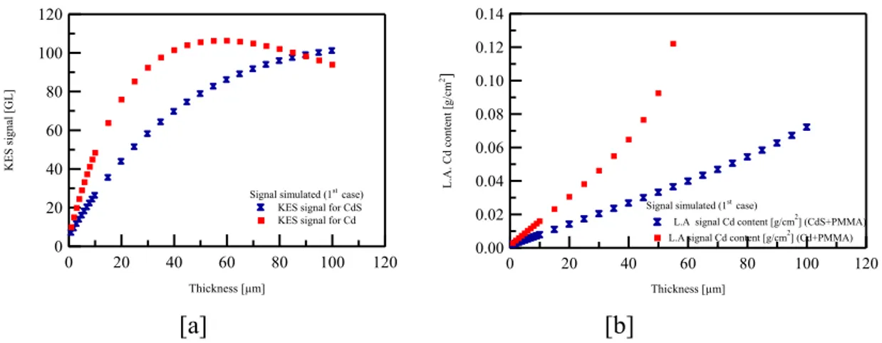
Figure 4.4: Linear KES and LA signals for the phantoms Cd+PMMA (red markers) and
CdS +PMMA (blue markers).(left) KES signal [GL] for both phantoms, [right] L.A. for mass density of Cd content in units [g/cm2].
Figure 4.5: Linear KES and LA signals for the phantoms Cd+PMMA (red marks) and CdS
+PMMA (blu marks).[a] KES signal [GL] for both phantoms, [b] L.A. for mass
density of Cd content in units [g/cm2].
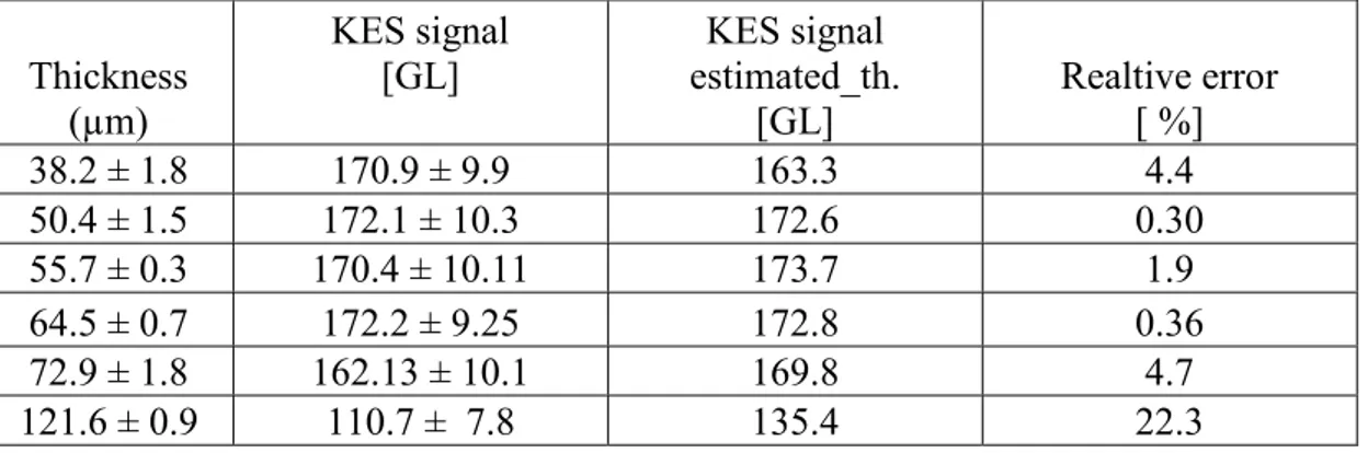
Table 4.1: Estimated values and experimental KES signal for 6 pieces cadmium pure. Table 4.1’: First case: Estimated values and experimental by L.A algorithm for 6 pieces
cadmium pure.
Table 4.2: Second case: Estimated values and experimental KES signal for 6 pieces
cadmium pure.
Table 4.2’: Second case: Estimated values and experimental by L.A algorithm for 6 pieces
cadmium pure.
CHAPTER 5
Figure 5.1: Spectra measured by CZT detector. Left: Experimental spectrum acquired by
CZT for Am-241. Right: Theoretical spectrum.
Figure 5.2: Output X- ray spectrum of Tungsten tube at 44kVp.
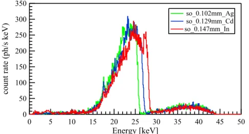
Figure 5.3: X- ray spectra transmitted by filter foils Ag, Cd and In (green-Ag, blue-Cd and
red-In) at 44kVp.
Figure 5.4: Subtracted X- ray spectra transmitted. The blue (Cd-Ag) spectra in energy
range E = [25.5-26.7] keV; red [In-Cd] energy range E = [26.7-27.9] keV.
Figure 5.5: X-ray spectrum of a W-anode x-ray tube at 44 kVp, with 1.55 mm Al of
additional filtration.
Figure 5.6: Transmitted spectra by filter foils Ag, Cd and In when 0.250mm and 0.060
mm Al are added for Ag and Cd respectively for W at 44kVp.
Figure 5.7: Subtracted X- ray spectra transmitted by filtering a W tube at 44kVp. The blue
(Cd-Ag) spectra in energy range E = [25.5, 26.7] keV; red [In-Cd] energy range E = [26.7-27.9] keV
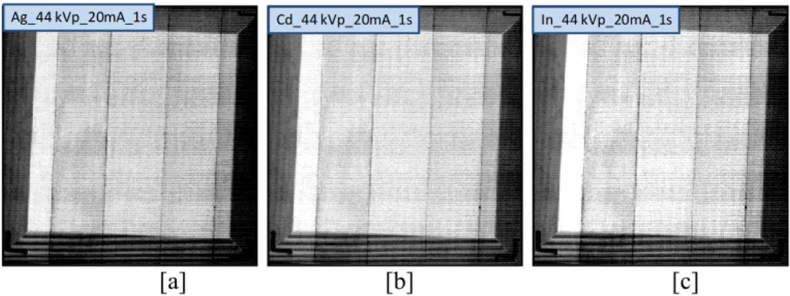
Figure 5.8 Images of 5section Cd_red canvas test by using W x-ray tube with additional
balanced filters. [a] Image acquired with Silver 0.102 mm; [b] Image with Cadmium filter 0.129 mm; [c] Image with Indium 0.147 mm.
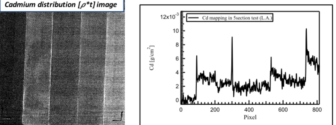
9 Figure 5.10: [a] Cadmium distribution image by KES subtraction of 5section canvas test.
[b] plot of Cd content along all the canvas test at selected region. [c] the Cd mean values in each section.
Figure 5.11: Image and the plot profile of image for cadmium content.(left) Cadmium
distribution image by L.A. (right) Plot of Cd content along all the canvas test at selected region.
Figure 5.12: Cd mean values in each section of canvas test and tabulated data. Figure 5.13: Images and Cd content in a selected region on image for second case.
(Left) KES results for cadmium content (right) L.A mean values in each section of canvas test 5section Cd red.
Figure 5.14: Images of 4strips Cd red on mylar support. [a] Image acquired with Silver
102 μm; [b] Image with Cadmium filter 129 μm; [c] Image with Indium 147 μm.
Figure 5.15: [left] Low Energy image (Cd-Ag image) [right] High Energy image (In-Cd
image).
Figure 5.16: KES results.[a] Image of Cadmium distribution (GL units [b] Mean
Cadmium [GL] content detected in each section, [c] results tabulated for each strip.
Figure 5.17: L.A results. [a] cadmium distribution image (g/cm2), [b] Mean Cadmium
[GL] content detected in each section, [c] results tabulated for each strip.
Figure 5.18: Cadmium distribution images for Y.N +Cd Red test canvas after processing.
(KES and LA processed)
Figure 5.19: Cadmium mapping on images of Y.N+Cd Red. [left block] Mean Cadmium
[GL] content detected along whole the canvas test by KES. [right block] Cd
content in (g/cm2) by L.A. signal.
Figure 5.20: Images of 6pieces Cadmium pure metal on PMMA support. [a] Image
acquired with Silver 102μm; [b] Image with Cadmium filter 129μm; [c] Image with Indium 147μm.
Figure 5.21: KES image of Cadmium 6pieces test phantom.
Figure 5.22: (left) Plot of KES signal versus thicknesses of Cd pure metal foils. (right)
Results tabulated for each strip.
Figure 5.23: Plot of KES signal for two experiments indicated by blue and red markers
and tabulated results.
10
Table 5.1: Total number of photons and the mean energy for W spectra and attenuated one
by filtration at 44kVp.
Table 5.2: The Cd mean values on each section and standard deviation.
Table 5.3: The Cd mean values for KES and L.A (second case) for 5section Cd red
sample.
Table 5.4: The Cd mean values on each section of images processed by KES and L.A
for Y.N + Cd red sample.
CHAPTER 6
Figure 6.1: The diagram of the production of the phenomenon of x-ray fluorescence. Figure 6.2: Principle of μ-XRF.
Figure 6.3: XRF spectra in semi log scale counts per second versus energy in keV. Red
spectrum form a Plexiglas sample. Blu one spectrum form Plexiglas + cooper wire.
Figure 6.4: [a] Schematic of ARTAX unit [b] Measuring head scheme, [c] CCD camera
image on bronze standard with an x-ray beam collimated by 1 mm collimator.
Figure 6.5: [a] Cross-section through an SDD X-ray detector, [b] Mode of operation of an
SDD-X-ray detector.
Figure 6.6: Photo by the CCD camera of copper wire positioning against the head
measurements
Figure 6.7: Measured scan profile from a line scan across a 50μm Cu wire for the Kα line. Figure 6.8: Image matrix as product of point spread function of XRF system in vertical
and horizontal direction. (Gaussian left and elliptical left)
Figure 6.9: [a] XRF spectrum of red cadmium sample, [b] Cadmium content for each
point scanned by XRF.
Figure 6.10: Average Cadmium content for each section. (Graphically presented (left) and
tabulated data (right).
Figure 6.11: Pazzini paint labelled at points scanned by XRF.
Table 6.1: Parameters for Gaussian fit for scan profiles of 50µm Cu wire. Table 6.2: Parameters for elliptical fit for scan profiles of 50µm Cu wire. Table 6.3: Cadmium net counts for 4 strips red cadmium sample.
Table 6.4: Cadmium net counts for Yellow Naples and red Cadmium sample. Table 6.5: Cadmium net counts for 6 pieces of Cd pure element.
11 CHAPTER 7
Figure 7.1: Cd average values of each section of Cadmium red 5sections canvas test. Figure 7.2: The correlation between KES and XRF technique for Cd content on
Cd_red5sections when no convolution is applied.
Figure 7.3: Cadmium distributed image, PSF of XRF signal (G.f), final image after
convolution.
Figure 7.4: The correlation between KES and XRF technique for Cd content on
Cd_red5sections when convolution is applied (Gaussian fit).
Figure 7.5: Cadmium distributed image, PSF of XRF signal (G.f), final image after
convolution.
Figure 7.6: The correlation between KES and XRF technique for Cadmium content on
Cd_red 5sections test when convolution is applied (elliptical fit).
Figure7.7: The correlation between L.A results and XRF technique for Cd content on
Cd_red5sections when no convolution is applied.
Figure7.8: The correlation between L.A results and XRF technique for Cd content on
Cd_red5sections when convolution is applied (Gaussian fit).
Figure7.9: The correlation between L.A results and XRF technique for Cd content on
Cd_red5sections when convolution is applied (elliptical fit).
Table 7.1: Tabulated results for both techniques KES and XRF for cadmium content in the
Cd red 5 section sample.
Table 7.2: Cadmium content estimated on KES (convoked with PSF of XRF signal, G.F)
and average XRF signal.
Table 7.3: Cadmium content estimated on KES (convolved with PSF of XRF signal,
Ellip.F) and average XRF signal(point)
Table 7.4: The correlation parameters obtained for KES measurements and XRF
measurements. KES = B*XRF + A
Table 7.5: The correlation parameters obtained for L.A applied in images and XRF
12
Introduction
Several techniques exist for mapping the element pigments on painting using the synchrotron light or quasi monochromatic sources. The aim of this thesis has been in application of K-edge subtraction technique to determine pigment composition in paintings by using common X-ray sources with balanced filters.
K-edge filtration is a well known technique and based on discontinuity in the attenuation coefficient due to photoelectric K-edge of the absorbing materials. A couple of filters with slightly different k-edge energies, if are with balanced thicknesses, can isolate spectra in a
narrow energy band. Quasi monoenergetic X-rays with a spectral width Ek that is the
difference in K-edge energies will be taken by subtracting images or spectral data [1][2][3]. Thus using filter foils with appropriate thicknesses with the K-edge absorption just below and above the K-edge energy of an element allow us evaluating the distribution of that element in whole paint.
Logarithmic subtraction of high- and low energy-images gives qualitative measurements but processing images with Lehmann algorithm gives information on the mass density of target element. Determination of cadmium element in its pigments it is performed by KES and Lehmann algorithm applied on digital images acquired.
The X-ray unit was the Tungsten tube filtered by a set of filters Silver Cadmium and Indium. Analytical simulations for foreseen signal produced on a CMOS RadEye200 digital detector are built to validate the technique.
Cadmium element in its pigments it is investigated in artificial phantoms and real paints In additional with the same samples complementary analyses are preformed with micro X-ray fluorescence spectrometry (µXRF) and it is determined a linear correlation between results.
13
CHAPTER 1
1. K-edge Imaging
In this chapter a theoretical introduction of main topics of this work will be presented. Conventional techniques in mapping elemental distribution in paints are mentioned with their advantages and disadvantages. Main procedure for elaborating digital images and algorithms for quantitatively evaluations are presented analytically.
1.1 Introduction to elemental mapping techniques on paintings: KES technique
The X-transmission radiography plays an important role in the examination of paintings. It provides information on execution techniques and under paintings based on X-ray attenuation by materials that compose the painting, however, does not provide elemental composition.
X-ray fluorescence spectrometry (XRF) and particle induced X-Ray emission (PIXE) are the main methods used for elemental composition of pigments in paintings. These techniques allow for detection of elements on a painting but their trade-off is the inspection is intrinsically local and takes a long time acquisitions.
The conventional K-edge subtraction technique it is used for tracing the contrast element in medicine [4] or elements with interest in mapping paintings [5][6] using the synchrotron light or quasi monochromatic sources.
This technique takes advantage of the sharp rise of X-ray absorption coefficient of the elements, the K-edge discontinuity. By using common X-ray tube three radiographies must be performed, including k-edge filters that bracket the edge energy of element of interest. Making the difference between adjacent K-edge filter images acquired by an integrator digital X-ray detector will be obtained the Low and High energy images which will present pseudo-monochromatic images. In this way, considering that Low and High energy image have information in narrow bin energy width (not more than 2keV) just below and above the edge energy of the element of interest means to have a high signal variation of target element and almost constant response from the background.
The images are processed by linear subtraction and Lehmann algorithm. Applying the linear subtraction on images qualitative information will be obtained in terms of distribution of element in digit numbers (gray level). Quantitative evaluation in terms of
mass density distribution (g/cm2) of the K-edge element will be obtained by Lehmann
14
In this work it is investigated the KES technique in elemental mapping of paintings by using a conventional X-ray tube with balanced filters. The advantage is that inspection is not intrinsically local but K-edge imaging allows to map elements in large area and in a short time.
1.2 Attenuation of X-rays
X ray is electromagnetic radiation with wavelength below 10 angstroms (10-9 m) and
generated by energetic electron processes. During interaction of X-rays with matter, X-rays possess intrinsic energy that may be imparted to the matter they interact with. Two main types of energy transfer that can occur when X-rays interact with matter are:
Ionization, in which the incoming radiation causes the removal of an electron from an atom or molecule leaving the material with a net positive charge.
Excitation, in which some of the X-ray’s energy is transferred to the target material leaving it in an excited (or more energetic) state.
Theoretically there are several processes that can occur when X-rays interact with matter, but only three of these processes are important which are:
Photoelectric effect Compton scattering Pair Production
Which process dominates is dependent on the mass absorption characteristics of the target (directly related to the atomic weight, Z) and the energy of the X-rays, shown schematically in the figure below.
Figure 1.1: Photoelectric effect, Compton effect and pair production and their dominance
15
They all contribute to the attenuation of intensity when an X-ray beam crosses the matter. The phenomenon is described by the Beer-Lambert law :
Where I is the number of photons emerging from the target, I0 the number of photons that
hit the target and μ is the total linear attenuation coefficient illustrated by Fig 1.2.
Figure 1.2: Illustrative scheme for the Beer-Lambert law.
Linear attenuation coefficient μ represents the sum of the coefficients related to three processes mention above: τ for photoelectric, σ for Compton and κ for pair production.
µ = τ + + κ (1.2)
For the range of energies lower than 100 keV and for relatively low atomic numbers (Z 20÷50) the photoelectric effect dominates and it is possible to consider total linear attenuation
Coefficient only related to τ. In general for radiography the mass absorption coefficient µ/
(cm2/g) are used, provided by NIST data base [7].
The Beer-Lambert law can be written:
When an X-ray beam crosses a compound C the mass attenuation coefficient will be calculated as the sum of absorption of each element taking into account their weight
fractions Wi:
µ
I0 I
16
Although the attenuation coefficient generally decreases with increasing photon energies, there are sharp discontinuities, known as absorption edges. The location of an edge along the photon energy axis depend on the atomic number of the absorber, and absorption edges have a number of important consequences, notably in the choice of a material as filters or intensifying screens [8].
The dependence of mass attenuation coefficient for X-ray with the energy for four elements it is presented in Fig.1.3 .The graph shows the decrease of mass attenuation coefficient when the energy is increased and also the K-edge discontinuity in correspondence of the photon interaction with K-shell electron.
Figure 1.3: Silver, Cadmium, Indium and Perspex X-ray absorption coefficient.
1.3 K-edge filter subtraction technique
Monochromatic X-ray beams are ideal for several applications in medical radiography, industrial inspection and culture heritage. Synchrotron facilities produce monochromatic X-rays but their use is very expensive. For this reason the development of alternative technique using conventional X-ray tubes and K-edge filters are needed. We have developed a new technique to shape X-ray spectra with k-edge filters having the same transmission for energies lower than the K-edge. By subtracting digital radiographies of a sample obtained with such filters we are able to obtain quasi or pseudo- monochromatic radiographies.
17 1.3.1. Theory
Let us consider the energy spectrum φ(E) of an X-ray photon beam as the distribution of the photon flux with respect to the energy. The total photon flux φ [photons/second] will
be given by the integration of the spectrum over the energy interval [Emin, Emax] where
φ(E)≠0:
If the photon beam is filtered with a material without K-edge in the energy range of interest
[Emin, Emax], having an attenuation coefficient and a thickness the transmitted
photon flux φf will be:
Considering now a set of materials having photoelectric K-edge at energy EKi within the
interval [Emin, EmaX] with attenuation coefficients and thickness chosen in such a
way they satisfy the following conditions:
(1) the thickness of each K-edge filter is such that the absorption is equal to that of
the filter without K-edge for energies lower than the energy of K-edge
(2) the transmission of edge filters is negligible for photons with energy above K-edge
When conditions (1.7) and (1.8) are satisfied, it is possible to demonstrate that the
subtraction of total fluxes of two filtered X-ray beams ( ) and ( ) will be:
18
This means that the difference of total fluxes is equal to the flux of photons with energies
higher than in the beam filtered with no k-edge. If we consider now two K-edge filters
with K-edge at energies < , both within the range [Emin, Emax] and thicknesses t1 and
t2, respectively , satisfying conditions (1.7) and (1.8), it is straightforward to demonstrate
that the subtraction of total transmitted flux to is:
Equation (1.10) shows that the difference between the total fluxes transmitted by two
properly selected K-edge absorbers is equal to the photon flux transmitted
from the filter with no K-edge in the range of energy between the two K–edge energies
and , (See Fig. 1.4).In other words, a single K-edge filtration works as a low-pass filter
for photon energies with a threshold value equal to the K-edge energy, while the subtraction of the transmitted beam by two different K-edge filters satisfying conditions (1.7) and (1.8), can be used as a band-pass filter for photons with energy within the two K-edges.
Figure 1.4: Schematic diagram of the k-edge subtraction technique.
Based on this theory, if we acquired the digital radiographies of a sample (or painting) by using properly chosen K-edge materials with a suitable detector, such as a Radeye200 CMOS pixeleted detector, subtraction between images will give quasi monochromatic images, presented as low and high energy image describe in paragraph 1.3.2. By processing images we can estimate the distribution of the target element in painting or sample test.
19 1.3.2. Analytical considerations in imaging with balanced filters
Let’s consider the experimental setup for acquisitions of digital radiographies as below:
Figure 1.5: Instrumental setup for K-edge imaging.
Images acquired by an in indirect detector system that is a scintillator based x-ray detector,
i.e RadEye200 CMOS detector coupled by a Gd2O2S (GOS) scintillator, will be modelled
mathematically.
By supposing a sample placed between continues X-ray source and the detector (Fig 1.5),
the average signal (image) <SGOS> obtained by CMOS sensor coupled by a GOS material
will be:
Where: φ0(E) is incident X-ray spectrum (photon fluence per energy interval ), second term
is the sum of the product of linear attenuated factor by thickness for each material that X- rays passes through, the terms underlined are respectively the fraction of photons attenuated in the detector and the amount of energy absorbed by the detector per attenuated
x-ray photon , ( , (E) are linear energy absorption and linear attenuation
coefficients of the GOS scintillator (cm-1)), γ is conversion factor of detector (converting
photon flux in gray values), E the energy for each incident X-ray photon in the range from
Emin to Emax, and index m for all materials that attenuate the beam. Theoretical formula
manly it is based on the absorption efficiency of the X-ray detector in which the signal is related to the total energy absorbed in the detector not in the number of X-ray photons [9]. If we have three K-edge filters (i.e., Silver, Cadmium, Indium), including K-edge target
element (cadmium) with edge energy respectively Ek1 < Ek2 < Ek3 , the image acquired by
Filter holder Sample
X-Source
Source- detector distance
Detector
20
detector for a sample positioned between source and detector for the first filter , Ik1 , will be
expressed as the integrated signal with Eq. (1.12).
Where µk1(E), tk1 are the linearattenuation coefficient (cm-1) and thickness (cm) for filter
material.
When we make the subtraction of images acquired for a sample using two edge filters that
satisfy the conditions (1.7) and (1.8), the low energy image IL in the energy interval
tha is the difference between two k-edge energies, will correspond to
integrated signal as follow:
Where is the mean energy value in the narrow interval defined by first two k-edge
filters. Considering that energy range is too close (less than 2 keV), transitions are based on mean value theorem for the definite integrals in a closed interval. So we can consider that low image it is an image like acquired in a quasi monochromatic energy beam with a
mean energy ).Integrated signal spectrally it is shown by gray
histogram on Fig. 1.6.
Figure 1.6: Pseudo-monochromatic spectra by using three adjacent balanced filters.
While for flat image that it is acquired when no sample it is between source and detector we can write: E0 Ek1Ek2 Ek3 (E) E Subtraction of k-edge 1-2, 2-3
21
In the same way we can write the expressions for the high image energy, IH, and high
flatimage which are integrated signals in the energy range above
the k- edge of the target e element:
Based on these mathematically modelled images we will introduce the procedure of corrections and processing images for obtaining information on element of interest in paintings.
1.4 Image processing
During the creation of a digital image from the detection of X-ray photons to the formation, there are several artefacts that cause either overestimation or under estimation of the signal level. These artefacts are noise and caused by different factors starting from the X-ray photons to the readout electronics, electromagnetic interference from external sources and the non linearity of CMOS detectors. For these reason image corrections it is necessary to avoid these noises [10].
1.4.1 Image corrections
For any images acquired by digital radiography the initial step is correcting them by two main artefacts: dark noise and fixed pattern noise (FPN).
Dark field correction (offset)
22
Thermal vibrations of charge carriers and depends on detector temperature and detection time. For this reason it is necessary subtracting the “dark image” by radiographic image, acquired at the same condition of time exposure when no X-ray photons hit the detector.
Flat field correction (gain offset)
The fixed pattern noise (or structure noise) describes the spatially fixed variations in the gain across detector. The noise sources might be variation in sensititivity between the digital sensor pixel elements, the phosphor screen granularity, or inhomogenity of x-ray field. For correcting images from these effects it is used the flat-field image correction. To perform this correction radiographic images are normalized, pixel by pixel, by a white field image, acquired at the same condition of beam flux and energy, position and acquisition time, with no sample.
The conventional method to correct a row images (I) is:
Where IC is the corrected image, D is the averaged offset image(dark image) acquired for
the same integration time, G is the averaged gain image (flat image) at the same irradiation
condition and the same integration time, and is the mean (or median) pixel value of G.
The subscript E denotes the incident exposure, while the subscripts t1 and t2 indicate the
times at which image sets are obtained [11].
1.4.2 Image subtraction and Lehmann algorithm
The principal of edge subtraction radiography is to make an element specific image using the absorbance image before (Low energy image) and after the absorption edge (High
energy image) of the element of interest. By using conventional X-ray tubes the low and high energy image will be obtained by subtraction of three images acquired when the
source is filtered by materials which have k-edge energies in the range very close to the element of interest and satisfied the conditions (1.7, 1.8 paragraph_1.3.1). Information on images, about the distribution of the element in a paint image, could be extracted in three ways; a) linear subtraction; b) logarithmic subtraction and c) Lehmann algorithm (LA). The two first gives qualitative analysis while the last gives quantitative analysis (the
surface density of target element in unit (g/cm2). For evaluation of cadmium element,
23
Linear subtraction (KES signal)
Considering the mathematical model of subtracted images obtained by integral detector
CMOS the low and high images (eq.1.13, 1.14) and flat low and high images, ,
(eq.(1.13’, 1.14’) and supposing that we image a “Test sample” with a thickness t and a total linear attenuation coefficient of µ (for simplified the situation) we can write [12]:
After correction of images (eq. 1.15), normalizing by flat image and making a linear subtraction of the low with high image, we obtain final KES image which it will depend on the linear attenuation of the k-edge element:
Lehmann algorithm
The dual energy algorithm introduced by Lehmann in medicine [13] consists of decomposing a single radiographic imaging into two components; the first one that gives
the mass density distribution of the K-edge element (ρx)el and the second one gives the
mass density distribution of all other materials in the sample (ρx)matrix. To estimate the
mass attenuation coefficient of the rest matrix a guess must be about the average composition. Often the rest matrix is represented by low Z equivalent material (water, carbon, Mylar, Perspex, etc.).Lehmann algorithm recently it is used for quantitative purposes in investigation of an element (pigment) in painting giving the mass density of
element in (g/cm2) [5], [14].
The signal in row images will be proportional to the number of photons that hit the detector after the transmission across the sample (Beer Lambert Law):
24
where N(E±) is the transmitted photons number per unit of area (correspond to image
acquired for sample), N0 incident photons number per unit of area (white field image), E+
and E− energies of monochromatic beams respectively above and below the K-edge of
target element), (μ/ρ)j are energy dependent mass absorption coefficients, (ρx)j are the
mass densities expressed in (g/cm2) and the subscript j denotes all the elements that
compose the sample under investigation.
Supposing that beam are monochromatic and with energies adjacent to K-edge of the target element means that mass attenuation coefficient of the target element will vary strongly
comparing to the other elements µ µ , that allow us writing the sum
in (eq.1.18) as sum of absorption of the target element (Cd) and the absorption of all the other elements as PMMA [15].
µ µ
If we explicit the expression (1.19) in two logarithmic equations respectively for Low(E-)
and High (E+) energies and resolve the system with two unknowns that are the mass
densities ( t)Cd and ( t)matrix :
µ ρ ρ µ ρ ρ µ ρ ρ µ ρ ρ
will be obtained two images as follow (1.21) and (1.22)
Where:
25
In this way applying the algorithm for each pixels in the row images two final images are obtained: the target element image (Cadmium) and of the residual one (PMMA).
Based on this algorithm, applying it on images acquired by using balanced filters the equivalent parameters will be:
Where are expressed by equations (1.14, 1.14’, 1.15, 1.15’).
1.5 Cadmium pigments
K-edge subtraction technique reveals useful information especially an artist’s techniques, pigments, and under paintings. Common elements in painting pigments are cadmium, mercury, lead, barium, antimony, and tin. Cadmium pigment has been chosen for investigation of K-edge imaging subtraction technique by using balanced filters.
The pigments of cadmium are inorganic colouring agents. Mostly used by the artists are cadmium yellow, cadmium orange and cadmium red which basically obtained by the cadmium yellow (cadmium sulphide) added some selenium in place of sulphur (cadmium selenide). The pigments are fine, discrete particles of coloured powder, with diameters of around 1 gm. The Cadmium pigments have also excellent heat stability which makes them essential in applications where elevated processing or service temperatures are encountered. It has been used by artists in contemporary age, since 1907. Artists who made frequent use of the yellow CdS pigments were Monet, Van Gogh, Miró, and Pablo Picasso. During the 20th century, the use of Cd pigments was expanded to include colouring of plastics etc. [16][17].
26
CHAPTER 2
2. X- Ray units and materials
In this chapter the base materials used for this work will be described with their specifications and the artefacts which will be in consideration to optimise them. The X – ray unit used for imaging was installed at Larix Laboratory, at Department of Physics in Ferrara.
2.1 X-Ray tube
X-ray source used is tungsten X-ray tube, M-143T manufactured by Varian1 with 0.63 mm
Beryllium window and a nominal focal spot size 0.1 x 0.35 mm2. The X-ray tube is
powered by a high-frequency 50 kHz, high-voltage generator, Compact Mammo-HF 2with
an adjustable voltage form 20 to 49kV. The setup for source has been chosen to obtain high flux by an anodic current, which is adjustable up to 120 mA.
Using Compact Mammo-HF allows working in two regimes: low current and high current. Low current (scopia)
This setting allows long exposition time, up to 300 second, and current supply is limited to low values, lower than 40 mA. Scopia setting is generally used for spectral analysis for a long exposition obtaining good statistics and low flux avoid saturation of the detector.
High current (grafia)
Allows short exposition time, 5 seconds maximum, but current higher than 40 mA. High current is needed for imaging, by taking into account that balanced filters will be used for obtaining images.
For measurements of real values of output spectra of tungsten tube when nominal values
are set up on Compact Mammo-HF2 generator measurements are performed by CZT
detector and it is calculated the endpoint energy spectrum by linear fitting using Igor program, presented in Tab. 2.1.
1Varian Medical systems
27 Table 2.1: Nominal values and real values estimated for the
X-ray unit used for imaging analysis. Nominal values
(kVp) Output spectrum (keV)
25.0 29.6 ± 0.9 27.5 32.5 ± 0.8 30.0 36.2 ±1.1 32.5 37.6 ± 1.1 35.0 43.7 ±1.1 37.5 46.1 ±1.1 40.0 45.5 ±1.0 2.2 Filters selection
In order to investigate a K-edge element in paintings, i.e the cadmium element with K-edge energy at 26.7 keV, three K-edge absorber materials were chosen: silver (Ag), cadmium (Cd) and indium (In) having k-edge energies respectively of 25.5, 26.7 and 27.9 keV. Filters foils in dimensions 5cm x 5cm are covered by a mylar paper and embed inside of aluminium holder with a window 4.5 x 4.5 cm (Fig.2.1).
Figure 2.1 Filter foils Silver Ag, Cadmium (Cd), Indium (In).
Their thicknesses has been chosen in accordance to the conditions (1.7, 1.8) and reported on Table 2.2.
Table 2.2: Filters characteristics.
Material k-edge energy (keV) Ideal Thickness T (µm)
Real thickness T (µm) Al no k-edge 1550 1550 ± 50 Ag 25.5 109 102 ±1.0 Cd 26.7 127 129 ±1.2 In 27.9 141 147 ± 1.8
28
In additional an aluminium filter it is used for removing the lower part photons energy and shifted the mean energy of photons near to K-edge energy of interest (26.7keV).
By subtraction of images acquired by the RadEye200 detector using each filter the low image and high image energy will be in the range 26.5 - 26.7keV and 26.7- 27.9keV, approximated with mean energy 26.1 and 27.3keV, described on the Tab. 2.3.
Table 2.3: Pigments of Cadmium element and X-ray energies.
Element Compound
Pigment name
K-edge energy
[keV] Low energy image High energy image
Cadmium
CdSe CdS
Cadmium red
Cadmium yellow 26.7 26.1 27.3
2.3 Phantoms and Test Pigments
For investigation of cadmium element in painting, canvas paint tests are prepared by Cultural Heritage Restoration and Conservation Centre "La Venaria Reale", in Turin, Italy and artificial phantoms are created in laboratory for the cadmium investigation as pure element.
These samples have been made with two main purposes: testing the technique ability to quantify the element content in the target and identify it when it is in different superimposed layers. The cadmium red tests have been realized on small canvas 10cm×10 cm in dimensions. The first one is divided in five sections with an increasing number of layers of cadmium pigment, as shown in Fig.2.2 [a]. In the second type two different pigments have been used, Cadmium red and Naples yellow (N.Y) and, in the central part of canvas, they have been superimposed as shown in Fig.2.2 [b]. Also a smaller target object, 10cm×8cm, has been realized with cadmium red pigment, in linseed oil on a mylar support Fig.2.2 [c].
29
For investigating the technique sensitivity for cadmium element (detection of minimal concentration by KES) also an artificial phantom is built in which 6pieces of pure cadmium foils with thickness in the range 35 to 130 µm are embed inside of two Perspex (PMMA) plates with dimensions 10cmx10cm with a thickness 0.6cm each shown in Fig_2.3.
Figure 2.3: 6_pieces pure cadmium phantom.
2.4 Integrated long travel stage
In order to keep fixed and moving the test samples in front of detector a stepper-motor
from Thorlabs' motorized stages LTS3001 it is used. The linear translation stages are
inclusive of the drive electronics which can either be driven via a PC or can be controlled manually.
LTS300 has a travel range 300mm with a maximum velocity 15 mm/s. The minimum incremental is 100 nm with a repeatable incremental movement of 4 µm. Absolute on-axis accuracy it is around 47 µm and the maximum percentage accuracy around 0.12 %. It has a maximum load capacity of 15 kg.
2.5 Detectors
The detectors used for investigation of k-edge subtraction technique have been CZT-100-XR as spectral detector and the remote RadEye200 (CMOS) imaging sensor.
2.5. 1 CZT spectrum detector
For measuring the spectra of tungsten (W) X-ray tube a cadmium zinc telluride detector
(CZT) was used. XR-100T-CZT is a solid-state detector with 5x5x2 mm3, 250 μm
beryllium window and a resolution of 940 eV FWHM at 59.54 keV [18]. The detection
30
efficiency is maximum between 10 and 80 keV and which means is approximately 100% in the energy range considered in this work with to maximum 44keV. In order to reduce
the X-ray photon fluxes on the detector a pinhole with a diameter of 0.137 mm2 has been
used.
2.5.2 The imaging detector
The Remote RadEye™ 200 sensor manufactured by Rad-icon Imaging Corp (CA, USA), is a two-dimensional CMOS photodiode array featuring up to matrix 1024x1000 pixels, with an active area 98.4mm x 96mm and pixel pitch 96μm. It is design to high resolution
radiation imaging for the energies range from 5 to 160 keV [19]. A Gd2O2S (DRZ-Std)
scintillator screen it is placed in direct contact with the photodiode array which converts incident x-ray photons to light. Each sensor it is enclosed with an aluminium cover and a graphite layer that shields the sensor against ambient light and protects the sensitive electronics from accidental damage. The analogue video signal is processed, digitized to 12-bit resolution with a dynamic range 4000:1 at frame rates 1.35 frames per second and it is transmitted to a PC. All three interface modules are compatible with ShadoCam image acquisition software, in which the output signal is the digital count value per pixel (in ADU, Gray Level) averaged over several region-of-interest areas in the image. Summary of features of Radeye200 is reported in Tab 2.4:
Table 2.4: RadEye200 specifications.
Parameters RadEye200 Units
Avg. Dark current (23°C)(1) 15 ADU/S(2)
Read noise (rms) <1 ADU
Dynamic range 4000:1
Digitization 12(3) bits
Conversion gain 1400(4) elec/ADU
Spatila resolution 5 Lp/mm
Max. frame rate 1.35 fps
x-ray energies 10-50 KVp
x-ray materials detecting
materil (thickness) Gd2O2S 46µm
(1)dark current doubles approx. every 8°C
(2)ADU = Analog-Digital Unit = 1 LSB (Least Significant Bit) (3)14-bit option available (LVDS & Ethernet interface only) (4)high-gain option (2x) available
31
CHAPTER 3
3.
X-ray performance evaluation of remote RadEye200 CMOS sensorImaging with solid state detector brings different artefacts that affect imaging and for this reason it is important the evaluation of their performance. In the following section CMOS architecture, working principle and some physical parameters will be discussed.
3.1 CMOS image sensor
The first solid-state image sensors were the bipolar and MOS photodiode arrays developed in the late 1960s [20]. During the years (1970) the device, CCDs as an analogue memory quickly became the dominant image sensor technology. In the early 1980s, it was entered CMOS image sensors and the further advantage of technology scaling, the digital pixel sensor (DPS), integrates an ADC at each pixel made it the main silicon technology drivers. The Figure 3.1 [21] [22] shows the structure of components of RadEye200 detector and the readout architecture of CMOS image sensor. CMOS sensor is direct coupling with a GOS (DRZ-Std) as scintillator. Two-dimensional array of Silicon photodiodes interface along with CMOS structures for scanning and readout. All support and control functions are integrated on-chip to minimize the amount of external circuitry needed to run the imager. The charge voltage signals from CMOS are read out one row at a time in a manner similar to a random access memory using row and column select circuits (see Fig 3.1 b).
[a] [b]
Figure 3.1: (a) Cross section with scintillator (b) Readout architectures CMOS.
RadEye200 sensors works based on clock signal which is a particular type of signal that oscillates between a high and a low state, to a maximum frame rate of 1.35 fps.
32
1024), which carried out collected charge at the end of the columns. The Horizontal register collects this signals and transfer charges to amplifier. The amplifier convert the charge derived from Horizontal register to a voltage signal.
3.2 Optimization of the system
There are a number of common metrics that are used for image sensors like quantum
efficiency, dynamic range, conversion gain, dark current, well capacity1. Taking into
account our purpose in mapping elements in an extended area of paintings it is necessary the evaluation of image sensor performance. Noises that affect more the signal in imaging are shot noise, fixed pattern noise, readout electronics, nonlinearity of CMOS sensor, etc.. Two main parameters can be important to be evaluated for optimizing CMOS image sensor: dark current and physical characteristics as MTF, NPS, DQE. In the following sections characterization in depth of the for dark current, MTF, NPS and DQE will be discussed.
3.2.1 Dark current
Dark current, i.e. charge generation with no incident light, is a parameter that is caused from electronic circuitry of the detector. It is a temperature dependent parameter and has a main affect in the linearity response or dynamic range of the sensor.
Also long exposure of detector vs. irradiation with x-ray will cause an increasing of the dark current and damaging the sensor. In that case the physical mechanism responsible for the increasing dark current is the charge build-up of positive charge in the oxide layer that directly modifies the underlying electric fields. Therefore modifying the charge density in
the depletion region and increasing the leakage current across the PN junction of the diode. In a CMOS transistor it means that the threshold voltage of the transistor slowly shifts,
until the device is either always on or completely closed off.
In addition electrons traps has been created by dose damage at the silicon- silicon dioxide interface which slowly de-trap into the pixel’s potential well causing dark current to increase. Digital devices are able to tolerate moderate amounts of threshold voltage shifts, enabling them to continue to function normally until the transistors stop working and the device fails [23]. To obtain a good signal-to-noise ratio is necessary to minimize dark current
33 3.2.2 Physical characteristics performance
The performance of RadEye200 we will see in terms of the calculation of detective quantum efficiency DQE that shows the ability of the detector to transfer the squared signal noise to ratio (SNR) from the input stage to output stage, MTF that describes the signal response at a given frequency and NPS that describes the amplitude variance at given frequency.
3.2.2.1 Detective quantum efficiency theory (DQE)
The DQE shows the ability of the detector to transfer SNR from its input to the output. It is defined as the square of the ratio of output signal- to-noise to input to signal to noise [24]:
The input signal consists of x-ray photons, which generally obey Poisson statistics, the so for the input signal-to noise could be written:
While the output signal-to-noise ratio is commonly measured by observing the signal and the noise power spectrum at the detector output. Expressed in terms of the input signal and the detector gain G,will be:
By combining the above equations we get
The detector gain and the noise power spectrum typically vary with spatial frequency. The modulation transfer function (MTF) is used to describe the relative decrease in gain with increasing spatial frequency. The final expression for calculating DQE then becomes
34
This expresses the fraction of input x-ray quanta used to create an image at each spatial frequency. The parameters as gain, MTF(f) and NPS(f) are easily measured simply by collecting enough images from the detector but input signal, it’s more difficult. Usually requires the use of conversion tables and references, and it is more difficult when the incident x-ray photons have different energies.
3.2.2.2 Determination of parameters MTF, NPS, Gain of detector, DQE
In the following sections the determination of MTF, NPS, gain of detector and DQE for remote RadEye200 will be discussed.
Modulation transfer function
An image sensor is a spatial (as well as temporal) sampling device. As a result, its spatial resolution is governed by the Nyquist sampling theorem that indicates: a continuous signal can be properly sampled, only if it does not contain frequency components above one-half
of the sampling rate1. Spatial frequencies in line pairs per millimetre (lp/mm) that are
above the Nyquist rate cause aliasing and cannot be recovered. Spatial resolution below the Nyquist rate is measured by the modulation transfer function (MTF), which is the contrast in the output image as a function of frequency.
The MTF of an idealized imaging system can be determined from the Fourier transform of the system's line-spread function (LSF). There are three experimental techniques to determine the LSF by a slit, wire, or edge imaging. [25], [26]. In the edge MTF technique, a "knife edge" made of a thin piece of strongly absorbing material is placed directly onto the detector and aligned at a slight angle typically (5-10°) to either the row or column direction. The edge should be as straight as possible (to within a fraction of the pixel size) and also as thin as possible to minimize shadowing in an off-axis measurement and scatter from the edge material at higher energies.
The measurements of MTF of radeye200 CMOs sensor it is used edge technique. Simply consists of taking an offset- and gain-corrected image of the edge using an appropriate combination of source kV, mA and integration time, in which we will have a good SNR. After correction of images (Eq.1.15), by making the differential along the row or column direction that is perpendicular to the edge, we obtain LSF of that particular row or column. The last step is to take the Fourier Transform of the LSF in order to obtain the MTF for the detector.
1 F
35 Figure 3.2: Presampling MTF for RadEye200 EV detector with GOS scintillator (Min-R
Med).
The Fig. 3.2 represents MTF curves for the remote RadEye 200 CMOS imaging sensor. There is no significant difference between the MTF along the row direction and that along the column direction. By curves it seems that resolution of detector is 5.2lp/mm.
Noise Power Spectrum
The Noise Power Spectrum describes the spectral decomposition of the noise variance in an image as a function of spatial frequency. It can be obtained by applying a two-dimensional Fourier Transform to an offset- and gain-corrected image from the detector. For the determination of NPS is enough to acquire two consecutive images from the detector and subtracts them. As NPS data are inherently noisy averaging over several data sets it is necessary in order to obtain a reasonably smooth curve.
If the two-dimensional NPS is symmetric, the analysis may be limited to either the row or the column direction by applying a one-dimensional Fourier Transform and averaging in the other dimension. This method yields a usable NPS curve from a single pair of images. In Fig.3.3 are presented the experimental NPS curves for remote RadEye200 detector measured for various exposure levels. For signal nearer to maximum of dynamic range of detector NPS curves do not change too much in their values (see Fig 3.3). Might be that saturation of signal is achieved before the limit of dynamic range of detector (1:4000 ADU).
36
Figure 3.3: Experimental NPS curves in horizontal and vertical directions.
Detector Gain
For determination of x-ray quantum flux incident on the detector two ways are possible: by measuring directly by ionization chamber or rely on physical models of the x-ray spectrum
from a typical x-ray tube 1. The magnitude of the resulting quantum flux then needs to be
calibrated against an actual measurement taken at the position of the detector in the experiment.
For measuring the gain of Radeye200 CMOS sensor it is used a Mo-Mo X-ray tube, at 30 kVp. Output signal for different input ray flux is presented in the Fig 3.4. The plot of X-ray response of the RadEye200 sensor shows a slight "S" shape, which is characteristic of the detector's intrinsic response curve.
Figure 3.4: RadEye200 response curve to different x-ray output.
37
Detective quantum efficiency
DQE is inverse proportional with NPS which express the distribution of the variance over spatial frequencies. After estimation of parameters the resulting DQE curves are shown in the Fig. 3.5 for RadEye200.
38
CHAPTER 4
4. Imaging simulations
In this chapter image simulations for cadmium element using
CMOS sensor
will bedescribed in additional to experimental tests to give definitions in analytical way of KES imaging technique by using balanced filters.
4.1 Image simulation for Cadmium pure element and Cadmium yellow
In order to estimate the real cadmium element in paintings, preliminary calculations have been performed for a similar situation like in the experimental tests.
Theoretical simulations will be discussed for a range of cadmium as pure element and as compound pigment, yellow cadmium CdS. Cadmium yellow it was chosen instead of red cadmium (CdS+CdSe) for simplify simulations. The target sample supposed it was Cd pure element or CdS as layers supported on a PMMA plate with a thickness 0.4cm.
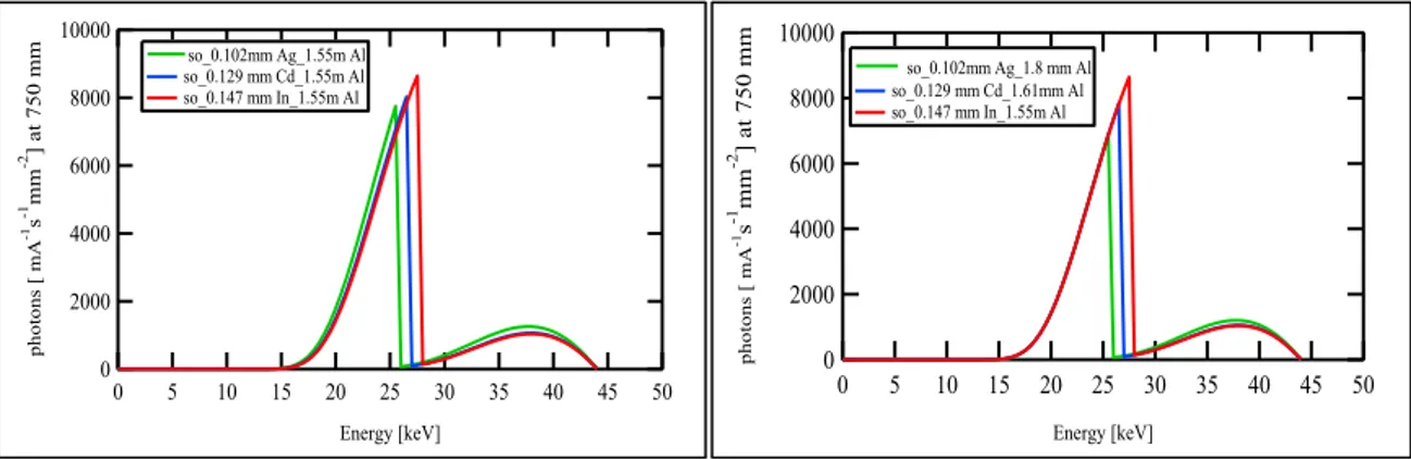
Image simulations have been done considering experimental setup scheme for K-edge subtraction imaging (Fig.4.1), with an X- ray source Tungsten, filtered by Ag, Cd and In materials with correspondent thicknesses 0.102, 0.129, and 0.147mm and imaging receiver the integrator CMOS 200 sensor.
Figure 4.1: Experimental setup scheme.
Calculations were performed based on Eq. 1.12, which gives the average signal converted in image by a CMOS sensor coupled by a GOS scintillator. In additional an aluminium filter will be added for removing lower energy photons.
Filter thicknesses for Ag, Cd, and In are chosen satisfying the conditions (1.7 and 1.8) but are not perfectly in ideal one (the ideal thickness must be for Ag, Cd and In 0.109, 0.127 and 0.141 respectively). To achieve the ideal thickness for balanced filters (or Ross filters) it is difficult so some techniques are suggested by literature for correcting the balance errors [27, 28].
In our case a prefiltration with a low Z material (Al material) for Cadmium and Silver filtration was used. (The differences in transmitted spectra because of not ideal thicknesses are eliminated by adding an equivalent low Z material filters in additional to k-edge filter). In this way the not overlapped spectrum transmitted by each k-edge filter in the range from the minimum energy till to their k-edge energy will be “disappear”, and a good
39
overlapping brings a good cancelation of photon energies out of band-pass defined by K-edge filters (refer to Fig 4.2). These two cases will be discussed below.
4.2 Theoretical Tungsten spectrum source and filtration spectra
For this purpose theoretical source spectrum for a W tube at 44 kVp, with anode angle 10
degree for time 1s is provided by Spectrum Processor1, while the total attenuation
coefficients μ/ρ (cm2/g) for the materials that X- ray beam passes through, are taken from
XMuDat2.
In the Fig 4.2 Spectrum data for the tungsten source is presented graphically and filtered spectra are shown in sequent figure (Fig 4.3).
Figure 4.2: Theoretical W spectrum from spectrum processor at 44 kVp.
Figure 4.3: Theoretical W spectrum at 44 kVp filtered by Silver, Cadmium and Indium
filter. Left: transmitted spectrum filtered by 1.55mmAl in additional to each k-edge filter (in correspondence with the colour). Right: transmitted spectra with k-filters+1.55mmAl and an additional for Cadmium filter of aluminium 0.06mm and 0.250mm for Ag.
1K Cranley, B J Gilmore, G W A Fogarty and L Desponds. Rep.No78.Catalogue of diagnostic X-Ray Spectra and Other Data, September, 97
2XMuDat. J Hubbel, S M Seltzer. NISTIR, 5632,1995
900x103 800 700 600 500 400 300 200 100 0 photons [ mA -1 s -1 mm -2 ] a t 750 mm 50 45 40 35 30 25 20 15 10 5 0 Energy [keV] source spectrum (W at 44kVp) 10000 8000 6000 4000 2000 0 photons [ mA -1s -1mm -2] a t 750 mm 50 45 40 35 30 25 20 15 10 5 0 Energy [keV] so_0.102mm Ag_1.55m Al so_0.129 mm Cd_1.55m Al so_0.147 mm In_1.55m Al 10000 8000 6000 4000 2000 0 photons [ mA -1s -1 mm -2 ] at 7 50 mm 50 45 40 35 30 25 20 15 10 5 0 Energy [keV] so_0.102mm Ag_1.8 mm Al so_0.129 mm Cd_1.61mm Al so_0.147 mm In_1.55m Al


![Figure 5.10: [a] Cadmium distribution image by KES subtraction of 5section canvas test](https://thumb-eu.123doks.com/thumbv2/123dokorg/4727055.45910/52.892.316.604.477.1045/figure-cadmium-distribution-image-kes-subtraction-section-canvas.webp)