Dipartimento di Fisica
Dottorato di Ricerca in
SCIENZE E TECNOLOGIE FISICHE, CHIMICHE E DEI MATERIALI
IN CONVENZIONE
CON IL CONSIGLIO NAZIONALE DELLE RICERCHE
CICLO
XXIX
Smart composite nanomaterials for atmospheric pollution detection
Settore Scientifico Disciplinare CHIM/05
Coordinatori
Supervisori/Tutor: Ch.mo Prof. Nicola Pirrone
Dott.ssa Antonella Macagnano
Dott.ssa Barbara Richichi
Coordinatore
di dipartimento: Prof. Vincenzo Carbone
Dottoranda: Dott.ssa Viviana Perri
To myself, to my determination and to those who have always believed in me
I
Index
Acknowledgements Preface 1 Introduction 3 CHAPTER 1Nanotechnology: nanomaterials, nanocomposite, applications
and potentiality 6
1.1 Nanotechnology 6
1.1.1 Application and potentiality 9
1.2 Nanostructured materials (NSMs) 12
1.2.1 Classification of nanostructured materials (NSMs) 13
1.2.2 Synthesis: Top-down and Bottom-up approach 16
1.3 New nano-heterogeneous systems: Nanocomposite 17
1.3.1 Nanocomposite thin film fabrication methods 23
1.3.1.1 Physical Vapor Deposition 24
1.3.1.2 Chemical Vapor Deposition 28
1.3.1.3 Wet-chemical deposition 29
1.3.1.4 Electrospinning: one-dimensional composite
nanomaterials creation 32
1.4 Characterization techniques 32
1.4.1 Morphological characterization 33
1.4.2 Chemical analysis by spectroscopic techniques 37
References 41
Introduction 50
CHAPTER 2
Electrospinning and nanofibers 52
2.1 History of electrospinning 52
2.2 Electrospinning Process 54
2.3 Electrospinning: Parameters process 56
2.3.1 Polymer solution parameters 57
2.3.1.1 Molecular weight and solution viscosity 57
II
2.3.1.3 Solution Conductivity 59
2.3.1.4 Dielectric effect of solvent 60
2.3.2 Process parameter 61
2.3.2.1 Voltage 61
2.3.2.2 Feed rate 63
2.3.2.3 Temperature 64
2.3.2.4 Effect of collector 64
2.3.2.5 Diameter of pipette Orifice/ Needle 65
2.3.2.6 Distance between tip and collector 66
2.3.3 Ambient Parameters 66
2.3.3.1 Humidity 67
2.3.3.2 The composition of the atmosphere 68
2.3.3.3 Pressure 68
2.4 Creation of different nanofibers 68
2.5 Functionalization of nanofiber: methods combined with electrospinning in order to produce 1D functional composite
nanomaterials and thin films 70
2.5.1 Nanocomponents inclusions 72
2.5.2 Surface modification of nanoparticles 72
2.5.3 Chemical functionalization of the surface of the
nanoparticles 73
2.5.4 Surface modification of TiO2 nanofibers with a bi-
functional chemical reagent, and decoration with
nanoparticles 74
2.5.5 Functionalization of TiO2 nanofibers through physical
adsorption of nanoparticles 74
2.5.6 Nanoparticles dispersible in aqueous or high-polar solvents 75
2.5.7 UV-Photoreduction 75
2.5.8 Acid gas-surface reaction 76
2.5.9 Codeposition 77
2.6 Applications of electrospun nanofibers 78
2.6.1 Filtrations 78
2.6.2 Affinity membranes and recovery of metal ions 80
2.6.3 Tissue engineering scaffolds 80
2.6.4 Wound healing 82
2.6.5 Release control 83
2.6.6 Catalyst and enzyme carriers 84
2.6.7 Sensors 85 2.6.8 Energy applications 87 2.6.8.1. Catalysis 87 2.6.8.2 Solar cells 88 2.6.8.3 Batteries 88 References 90
III
Introduction 106
CHAPTER 3
Gas sensors 107
3.1 Definition of Gas Sensors 107
3.2 Chemically interacting materials: polymers, macromolecules
and different types of nanocomposite films 110
3.2.1 Polymers 111
3.2.1.1 Chemical sensors based on polymers 112
3.2.2 Differents types of nanocomposite films 115
3.2.2.1 Metal-metal oxide nanocomposite films 115
3.2.2.2 Mixed metal oxides 117
3.2.2.3 Polymer-metal or metal oxide 117
3.2.2.4 Chemical sensors based on metal oxide
semiconductors nanocomposites 119
3.2.2.5 Carbon nanotube based on nanocomposite films 121
3.3 Classification of chemical gas sensors 122
3.3.1 Optical sensors 122 3.3.2 Conductometric sensors 123 3.3.3 Capacitive Sensors 124 3.3.4 Mass sensors 125 3.3.5 Electrochemical sensors 125 3.3.6 Magnetic sensors 126 3.3.7 Temperature sensors 127
3.4 Nanostructured commercial sensors 127
3.5 Characteristic parameters of chemical sensors 132
3.5.1 Calibration curve 132
3.5.2 Reversibility 133
3.5.3 Sensibility 133
3.5.4 Selectivity and cross-sensitivity 134
3.5.5 Resolution and detection limit 135
3.5.6 Accuracy and reproducibility 136
3.5.7 Drift 137 3.5.8 Precision 137 3.5.9 Repeatability 138 3.5.10 Stability 138 3.5.11 Error 138 3.5.12 Linearity 138 3.5.13 Hysteresis 139 3.5.14 Detection limit 139 3.5.15 Dynamic range 140 3.5.16 Response time 140
IV
3.5.17 Recovery time 140
3.5.18 Working temperature 140
3.5.19 Life cycle 141
3.6 Characteristics of chemical gas sensors 141
3.7 Mechanism of gas detection 142
3.7.1 Adsorption Processes 143
3.7.1.1 Adsorption isotherm 145
3.7.1.2 Langmuir isotherm 147
References 150
CHAPTER 4
Nanacomposite materials designed and investigated for sensing
materials 158
4.1 Optical nanoparticles: Quantum Dots (QDs) 158
4.2 Optical properties of QDs 158
4.3 Core-shell structures 162
4.4 Synthesis CdSe/ZnS QDs 165
4.4.1 Synthesis CdSe in organic media 165
4.4.2 Coating of the CdSe core with ZnS layer 168
4.4.3 Synthesis CdSe/ZnS in aqueous media 169
4.5 The role of the ligands 170
4.6 Doping of metal oxides with QDs 171
4.7 Semiconductor-metal nanocomposites 172
4.7.1 Chemical structure of TiO2 173
4.7.2 Heat treatment of TiO2 175
4.8 Doping of metal oxides with metallic nanoparticles 176
4.8.1 Doping of TiO2 nanoparticles and nanofibers with gold
nanoparticles 177
4.9 Development of blends of polymer nanofibers 179
References 181
Introduction 189
CHAPTER 5
V
5.1 CdSe/ZnS-TiO2 nanofibers: a suitable combination for a low
cost and effective optical sensor device to reveal NH3 and H2S
traces in the atmosphere 191
5.2 Materials, methods and characterization 195
5.2.1 Chemicals 195
5.2.2 Synthesis of CdSe/ZnS core/shell nanoparticles 195
5.2.3 Electrospinning of titania nanofibers 196
5.2.4 Titania nanofibers labelling with CdSe/ZnS QDs 197
5.3 Morphological and optical characterization of samples 197
5.4 Results and discussion 199
References 212
Introduction 216
CHAPTER 6
Study and design of a potential biodegradable chemical sensor to measure gas and volatile organic compounds (VOCs) in
moistened environments 219
6.1 Properties of materials selected and used: PANi, PHB and IDEs 219
6.2 Materials, methods and characterization 222
6.2.1 Materials 222
6.2.2 Methods 223
6.2.3 Characterization 225
6.3 Results and discussion 225
6.4 Conclusions 241
References 243
Introduction 248
CHAPTER 7
Development of chemoresistors employing TIO2 nanofibers photocatalytically decorated with Au-nanoparticles for to detect
mercury vapors in the atmosphere 253
7.1 Materials, methods and characterization 253
7.1.1 Chemicals and IDEs 253
7.1.2 Electrospinning technology: solution and deposition 254
VI
7.1.4 Fibers characterization 256
7.2 Electrical measurements 257
7.3 Hg0 vapor measurements 258
7.4 Results and discussion 260
7.4.1 Morphological investigation of AuNPs/TiO2 nanofibrous
layer 260
7.4.2 UV-Vis spectra AuNPs/TiO2 nanofibers before and after
exposure of Hg° 267
7.4.3 Electrical and sensing features 270
7.5 Conclusions 289
References 291
Introduction 296
CHAPTER 8
Novel passive sampling systems of mercury based on
nanostructured materials 299
8.1 International initiatives and programs: UNEP, GMOS, GEO,
GEOSS 299
8.2 Nanostructured passive samplers advantages 301
8.3 Basic elements of passive air sampling 301
8.4 Materials, methods and characterization 302
8.4.1 Chemicals 302
8.4.2 Study, designing and development of different strategies for the manufacture of novel passive sampling systems of
elemental mercury 303
8.4.2.1 First strategy: Passive samplers based on nanofibers 303
8.4.2.2 Second strategy: Passive samplers based on
nanofibers free standing 304
8.4.2.3 Third strategy: Passive samplers based on
nanoparticles 305
8.4.2.4 Fourth strategy: Passive samplers based on
nanoparticles and a thin quartz filtering support 307
8.5 Morphological and Optical characterization of samples 308
8.6 Results and discussion 310
8.7 Passive sampling materials 314
8.7.1 Elemental mercury sampling 316
VII
Acknowledgements
At the of this long and wonderful experience, I feel obliged to express my gratitude to the people who have supported me in every way during the months of laboratory work and for the preparation of this thesis work, especially in the hardest and most delicate moments; it is on these occasions that a word of comfort can be useful to regain strength and move on.
A special thanks to Professor Nicola Pirrone for giving me the opportunity to attend an important and authoritative scientific reality as the Institute of Atmospheric Pollution of National Council of Research and for not having never miss his support whenever I needed.
A big hug filled with gratitude to Dr. Antonella Macagnano and to all scholars and technicians of the structure for welcoming me in the group with loyalty, professionalism and sympathy and for the invaluable advice for my final work. The same dose of affection comes to Dr. Barbara Richichi and the wonderful group of researchers, now become very dear friends, of the Scientific Centre of the University of Florence in Sesto Fiorentino.
I will never forget the long study days spent together and the moments of leisure who saw me grow up, meet new people, visit wonderful places and broaden my knowledge in a field of science almost unknown.
Thank you, finally, to my wonderful family for financial, moral and psychological support and for believing and supported all my choices of life, work and study. The same family that already on the occasion of my graduation had answered quietly and proudly to who, some years before, had not confided in me to achieve important and prestigious objectives. Mom and dad taught me that work and the sacrifices always pay and also this time they have "seen along."
1
Preface
The content of this Ph.D thesis has been organized as follows: after a brief
introduction on nanotechnologies and their main applications, the
electrospinning technology will be described as a successful strategy to create smart and ultrasensitive nanosensors. The main characteristics of gas sensors will be listed in Chapter 3 focusing on sensitive nanocomposite materials designed for chemical sensors, more specifically suitable polymers as polyaniline and poly-3-hydroxybutirrate (PANi and PHB), semiconductor metal
oxides (QDs, TiO2) and gold nanoparticles (AuNPs). In subsequent chapters it
will be described in detail the manufacture, the characteristics, the detection mechanism and numerous advantages of nanosensors obtained using materials just mentioned. As will be described in Chapter 5, the combination of suitably functionalized nanofibers of titania with core/shell QDs nanoparticles has allowed to obtain a chemical sensor, in the solid state, capable to detect nitrogen compounds into the atmosphere. The resulting fibers were studied as potential optical sensors due to the quenching of the fluorescence after interaction with the
gas (NH3). Ammonia, furthermore, with other pollutants such as VOCs
(triethylamine and acetic acid), have been detected using a biodegradable chemical sensor, described in Chapter 6, obtained by electrospinning technology depositing a polymer blend containing polyaniline and poly-3-hydroxybutirrate (PANi/PHB) on chemoresistors (IDEs). Chapters, 7 and 8 respectively, will focus on two new detection systems, an active sensor (IDEs) and a passive sampler for the monitoring of elemental mercury (Hg°), another abundant pollutant in the atmosphere. For the manufacture of both systems, the photocatalytic properties of titania have been exploited providing a selective growth irradiation of gold nanoparticles, using a precursor of the gold nanoparticles (AuNPs) and a suitable organic capping reagent under UV-light
2
exposure. Finally, in summary and conclusions, all the research activity will be resumed enhancing the novelty, the potentials and the future perspectives.
3
Introduction
The exhaust from automobiles, emissions from manufacturing industries and factories, suspended particles and gases are among the unwanted substances that are deteriorating the quality of air around us and represent one of the major causes of air pollution. These harmful substances (solid particles, liquid droplets, or gases) can have adverse effects on humans and the ecosystem and are introduced in the air from various sources that can be of natural origin or man-made. Most of the pollution of the air is caused because of the ignorance and negligence of humans but it is also true that some time the air can be polluted by natural causes. Forest fires produce giant masses of smoke which tend to drift over nearby villages and cities. Occasional eruptions of volcanoes can eject huge amount of volcanic ash and lava onto the earth surface which introduces dust and smoke into the atmosphere thereby polluting the air. Natural air pollution can also be caused from the decay of rocks over time and the release of gases such as radon which has adverse effects on our health. Air pollutants can be distinguished into two types: primary and secondary pollutants. Primary pollutants are usually produced from a process, such as ash from a volcanic eruption. Other examples include carbon monoxide gas from motor vehicle exhaust, or the sulfur dioxide released from factories. Secondary pollutants are not emitted directly. Rather, they are formed in the air when primary pollutants react or interact. Ground level ozone is a prominent example of a secondary pollutant. Some pollutants may be both primary and secondary, they are both emitted directly or formed from other primary pollutants. Major primary pollutants produced by human activity include:
carbon dioxide (CO2); sulfur oxides (SOx), particularly sulfur dioxide;
nitrogen oxides (NOx) , particularly nitrogen dioxide; carbon monoxide (CO);
volatile organic compounds (VOC), VOCs are a well-known outdoor air
4
(NMVOCs); particulates, alternatively referred to as particulate matter (PM), atmospheric particulate matter, or fine particles, are tiny particles of solid or liquid suspended in a gas; persistent free radicals; toxic metals, such as lead and mercury, especially their compounds; chlorofluorocarbons (CFCs);
ammonia (NH3), emitted from agricultural processes; odors, such as from
garbage, sewage, and industrial processes; radioactive pollutants, produced by nuclear explosions. Secondary pollutants include: particulates created from gaseous primary pollutants and compounds in photochemical smog; ground
level ozone (O3) formed from NOx and VOCs. Many studies have confirmed
that indoor air quality is highly affected by outdoor air quality. Therefore, to solve our pollution problems, both indoor and outdoor environment should be considered. A number of air pollutants have been recognized to exist indoors,
including NOx, SO2, O3, CO, volatile and semi-volatile organic compounds
(VOCs), PM, radon, and microorganism. Some of these pollutants (e.g., NOx,
SO2, O3, PM) are common to both indoor and outdoor environments, and
some of them may be originated from outdoors. These air pollutants can be inorganic, organic, biological or even radioactive. Their effect on humans depends on their toxicity, concentration and exposure time, and may vary from person to person. The most common effect is called sick building syndrome (SBS), in which people show effects such as irritation of nose, eyes and throat, skin ailments, allergies, and so on. The cause may not be identified, but the syndrome may disappear after that an affected person leaves the office or building. Indoor air quality can be improved and SBS can be reduced when the ventilation rate of the room is improved (Wargocki, P. et al., 2000). The indoor air quality also affects the performance of workers and office staff. Wyon (2004) found that the performance of real office work would be significantly and substantially affected by changes in indoor environmental quality and that the work performance could be significantly enhanced by
removing common indoor sources of air pollution (Wyon, D. P., 2004). Air
5
diseases, cardiovascular and cancer, it is responsible of hundreds of thousands premature deaths in several countries in the world. WHO estimated in 2012 that air pollution claimed the lives of almost 3.7 million people around the world in just one year. This research project was carried out mainly at the Institute of Atmospheric Pollution Research of National Research Council (IIA-CNR) in Rome. Taking into account the need to support European directives, international treaties and programs of atmospheric and environmental pollution (i.e., UNECE-LRTAP, Minamata Convention, UNEP, GEOSS, Earth Cube) and the need to reduce investment costs and operating of observing sites in remote locations and difficult to access, the study has been focused on developing sensor devices low-powered and nanostructured composite materials for monitoring different pollutants and complex
environments, specifically, nitrogen derived gaseous pollutants (NH2, NO2,
NOx) and elemental mercury (Hg°). The goal of the research project has been
therefore to develop composite nanostructured materials for obtain "advanced" and "smart" sensors characterized by selectivity, sensitivity and small size, which do not require high investment and operating costs, which allow an environmental monitoring also in situ and that they are equipped by advanced interfaces for data transmission and their remote management.
6
Chapter 1
Nanotechnology: nanomaterials, nanocomposite,
applications and potentiality.
1.1 Nanotechnology
The term "nanotechnology" is gaining more and more popularity. It is, in fact, used to describe a variety of fields of research and development, often interdisciplinary (Laurecin, C. T. et al., 2009) and shall be defined as the science, engineering, and technology conducted at the scale that range between 1 to 100 nanometers. The prefix “nano” is derived from the ancient Greek “nanos”, meaning "dwarf”. Today, “nano” is used as a prefix that
means “billionth” or a factor of 10-9
. Coupling the word “nano” with the unit “meter” brings the term “nanometer”, which indicates a unit of spatial
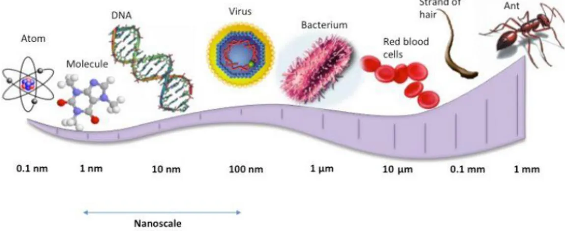
measurement that is one billionth of a meter. By comparison, the diameter of
an average human hair is approximately 100,000 nm and a red blood cell is about 7,000 nm in diameter (Alberts, B. et al., 2004) (Figure1.1).
7
The "nanoworld" is thus populated by objects such as atoms, molecules, which can be properly assembled into "nanostructures". The nanotechnology
objectives are precisely realize, study and take advantage of the nanostructures.
The concept of nanotechnology was introduced for the first time by the physicist Richard Feynman, at the American Physical Society meeting at the California Institute of Technology (CalTech) in 1959, with a talk entitled “There’s Plenty of Room at the Bottom”. In his talk, Feynman described a process in which scientists would be able to manipulate and control individual atoms and molecules (Feynman, R., 1960). However, the modern era of nanotechnology began only in 1981, when the scanning tunneling microscope that could "see" individual atoms was developed and used (Binnig, G. et al., 1982). Already in 1974, it was, however, patented the first molecular electronic device by IBM (Eigler, D. M. et al., 1990). In 1985 he came to the discovery of fullerene (Thrall, J. H., 2004) and subsequently to carbon nanotubes (Ajayan, P. M. et al., 1999). The fullerene, together with the graphite and the diamond, is the only stable molecule composed solely of carbon atoms. It is also referred to as C60 carbon, as constituted by sixty carbon atoms and has the shape of an icosahedron which has been truncated to 12 vertices. In 1991 Sumio Iijima, researcher of NEC Corporation, discovered that the carbon could be organized, as well as in spheres, even in pipes from a few nanometers variable diameter. These structures are called nanotubes and represent the absolute best known nanomaterials (Ajayan, P. M. et al., 1999). Subsequent developments have led to nurture interest in the single-electron devices (Konstantin, K., 1999), devices based on DNA (Christof, M. et al., 2002), molecular electronics and has led to study nanocrystals and quantum
dots (Rao, C. N. R. et al., 2004; Smith, M. et al., 2009). However,
nanotechnology anticipated applications range from optoelectronics (Gisev, A. I. et al., 2006; Kamat, P. V. et al., 1997), single electron transistors and light emitters (Klein, D. L. et al., 1997; Liu, C. H. et al., 2007), non-linear optical
8
devices (Wang, Y., 1991; Gleiter, H., 2000), catalysis (Skorokhod, V. et al., 2001; Pokropivny, V. V. et al., 2007), solar energy conversion (Hagfeldth, A. et al., 2000; Bueno, J. T. et al., 2004) photonic band gap materials (Moran, C. E. et al., 2004) and biomedical applications (West, J. L. et al., 2000; Salata, O. V., 2004). Innovation in knowledge and technology is the key element of the development and welfare of this new society; micro and nanotechnologies offer the ability to design and introduce innovation to the stairs, where the effects on the characteristics and performance of the products develop the maximum potential. One of the parameters that are strongly connected to miniaturization and nanotechnology is surface-to-volume ratio. This parameter is of fundamental importance in applications involving chemical catalysis and nucleation of physical processes. In general, surface area to volume ratio increases with a decrease in the characteristic dimensions of a material, and vice versa. A particle with a size of 30 nm has 5% of its atoms on its surface, whereas a particle of 3 nm has as much as 50% of its atoms on the surface (The Royal Society, 2004). Therefore, as the material size decreases, a greater portion of the atoms are found at the surface compared to those inside. It has also been found that some materials that are inert in their bulk form are reactive when produced in a nanoscale form. Therefore, nanomaterials have a much greater surface area per unit volume compared with larger particles. This leads to nanoparticles that are more chemically reactive, because molecules at the surface of a material do not have full allocation of covalent bonds and are in an energetically unstable state. Since many more molecules located at the surface are in energetically unstable states, nanomaterials are more reactive compared to the non-nanoscale material. With the high reactivity, almost all types of nanomaterials are capable of catalyzing reactions and free nanomaterials tend to agglomerate into bigger particles. Owing to the specific physiochemical properties of nanoparticles, they are expected to interact with substances such as proteins, lipids, carbohydrates, nucleic acids, ions, minerals and water present in food,
9
biological, or desalination processes. Other potential applications for this reactivity are drug delivery, clothing insulation, and more. Another factor that shapes the nanoscale behavior is the predominance of quantum effects that takes place as the electrons are confined by the dimensions of the nanostructure. As the size is reduced to a few tens of nanometers, the quantum effects starts to dominate the properties of matter, affecting the optical, electrical and magnetic behavior of materials (Ostiguy, C. et al., 2006). The development of knowledge and technology at the nanoscale is leading a revolution in the way we conceive, design and produce innovative products and systems. The materials sector is the one that more was influenced by the "nanotechnology revolution".
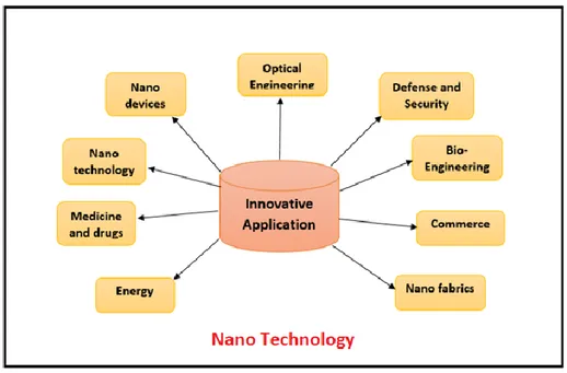
1.1.1 Application and potentiality
The concepts and fields of application of nanotechnology emerged in recent decades show a profound influence both on basic research both on industrial
technologies, directing them towards largely unpredictable directions. The
nanostructured products materials are polymeric materials, metallic materials, ceramic materials, semiconductors materials, magnetic materials and their benefits are particularly evident in the following areas (Figure 1.2):
Electronics: nanotechnologies can have a big impact on the
development, processing and application of electronic devices, such as nanodiodes, OLED, plasma displays, computer devices, chip design, nanotransistors, etc;
10
Energy saving: in the renewable energy improves energy efficiency in
production, and the absorption and storage of energy. Moreover, the miniaturization and the new materials increase the efficiency of the products. Nanotechnology applications can be found in the fields of photovoltaic solar cells, fuel cells, batteries, etc (Tian, B. et al., 2007);
Environment: the nanotechnology contributes significantly to
environmental sanitation and the solution of environmental problems. Recent results have shown great impact of nanomaterials used for environmental cleanup, such as the membranes for the purification and
de-contamination of underground water (Zhang, W. X., 2003; Long,
T. C. et al., 2006), the nanostructured traps for the removal of pollutants from industrial spills; the maintenance of industrial sustainability by significant reductions in material and energy used; reducing sources of pollution and increased recycling opportunities. In the security field they are important the detectors of chemical and biological agents;
Biotechnology:development of innovative biosensors and systems for
intelligent distribution of drugs. Develop biosensors means making molecular analysis; it is necessary to realize devices capable of interacting with complex organic molecules and give recognition signals, in real time related to the type of molecule and to its concentration. Technological perspectives and innovative potential applications for the analysis of DNA and RNA, proteins and other biological molecules or even cells;
Medicine: Nanotechnology provides new options for drug delivery and
drug therapies such as in cancer. Nanotechnology allows researchers to build nanosized devices that, when conjugated with antibodies, can
11
target tumor cells with high specificity and affinity. This enables drug delivery systems, in which small drug molecules can be encapsulated in micelles formed by nanomaterials that transport them to the desired location, thereby lowering the total drug consumption and side effects (Jain, K. K., 2010). Researchers have also developed an imaging technique to measure the amount of an antibody-nanoparticle complex that accumulates specifically in plaque, thereby serve as an early
diagnosis of atherosclerosis (Wickline, S. A. et al., 2006); Nano
dentistry will assist in the maintenance of complete oral health by employing nanomaterials, biotechnology, including tissue engineering, and ultimately, dental nanorobotics. New probable treatment opportunities in dentistry may include, local anesthesia, dentition renaturalization, permanent hypersensitivity cure, complete orthodontic realignments during a single office visit, covalently bonded diamondised enamel, and continuous oral health maintenance using mechanical dentifrobots. In medical filed, scientists have developed a surgical nanorobot, programmed or guided by a human surgeon that can act as a semiautonomous on site surgeon inside the human body, when introduced into the body through vascular system or cavities. Such a device could perform numerous functions such as searching for pathology and then diagnosing and correcting lesions by nanomanipulation, coordinated by an on-board computer while maintaining contact with the supervising surgeon via coded ultrasound signals (Robert, A. et al., 2005).
Fabrics: Nanotechnology is also applicable in clothing. The properties
familiar materials are being changed by manufacturers who are adding nanosized components to conventional materials to increase performance.
12
Food and agriculture safety: This technology is used to improve the
quality of food. There are multiple applications of nanoparticles in food and agriculture safety.
Automotive and aeronautics industries: tires reinforced with abrasion
resistant nanoparticles and recyclable; paint dust; plastic non-flammable and low cost; electronic control; coatings and self-repairing materials;
Figure 1.2: Example of some fields of nanotechnology applications
1.2 Nanostructured materials (NSMs)
One of the basic results of the materials science is the insight that most properties of solids depend on the microstructure. A reduction in the spatial dimension, or confinement of particles or quasi-particles in a particular crystallographic direction within a structure generally leads to changes in
13
physical properties of the system in that direction (Pokropivny, V. et al., 2007). An object that has at least one dimension in the range of 1-100 nm is defined a nanostructure. Nanostructured materials have been shown to exhibit high strength, increased diffusivity, reduced sintering temperatures, useful catalytic properties, and attractive physical properties. Due to their novel and improved properties and varied potential applications in different fields of technology, these materials are attracting increasing attention from researchers all over the world. Some excellent reviews are available in the literature detailing the synthesis, characterization, properties, and potential applications of nanostructured materials (Suryanarayana, C., 1995; Suryanarayana, C., 2005).
1.2.1 Classification of nanostructured materials (NSMs)
Nanoscale materials have always existed from both natural and anthropogenic sources (Klaine, S. J. et al., 2008). The fine fraction of desert sand, fumes originating from volcanic activity or from forest fires, and certain atmospheric dusts, all represent nanoparticles produced by nature (Ostiguy, C. et al., 2006). In addition, a majority of biological processes occur at the nanoscale range and can be considered as nature’s own nanotechnology. For instance, the ribosome acts as a nanosized factory combining amino acids in a specific order to create proteins (Ashby, M. F. et al., 2009), and hemoglobin, the oxygen-transporting protein found in red blood cells, is 5.5 nm in diameter. Other nanomaterials are unintentionally released into nature from anthropogenic sources, which is byproducts of human activity, such as car exhaust, industrial emissions and welding fumes (Nowack, B. et al., 2007, Ostiguy, C. et al., 2006). Nanomaterials can be classified in a number of ways, inasmuch, the research and the rapid development of nanotechnology
14
have resulted to the creation of different nanomaterials in terms of materials types, physical dimensions and structures. First classification of nanostructures materials (NSMs) was proposed by Gleiter in 1995 (Yoffe, A. D., 1993) and further was explained by Skorokhod in 2000 (Reetz, M. T. et al., 1995). Nanomaterials can be categorized primarily according to their chemical composition (Handy, R. D. et al., 2008; Buzea, C. et al., 2007). This classification separates nanomaterials into broad categories such as carbon-based structures including CNTs and fullerene C60; metal-containing
nanoparticles including metal oxides, such as titanium dioxide (TiO2); or
semiconductor nanocrystals, also known as quantum dots (Figure 1.3).
Figure 1.3: Natural and engineered nanoscale substances (Farré et al., 2009)
Another way of categorizing nanomaterials is based on their dimensionality (Buzea, C. et al., 2007, Krug, H. F. et al., 2011). There are two main types of nanomaterials, according to the International Organization for Standardization (ISO/2011), nanostructured materials and nanoobjects (Figure1.4).
15
Figure 1.4: The ISO/2011 definition of nanostructures material and nanoobjects. The shape of nanoobjects reflects the number of dimensions confined to the nanoscale (Krug and Wick, 2011).
Nanostructured materials include nanoporous materials (which have nanosized pores within particles that may or may not be of nanoscale dimensions), nanocrystalline materials (which have nanosized crystalline grains within particles that may or may not be of nanoscale dimensions), and complex fluids
16
containing nanosized objects. Therefore they comprise a broad class of materials that contain nanosized structures, without necessarily having an
overall nanoscaled size.The classification of nanoobjects essentially depends
on the number of dimensions which lie within the nanometer range, separating them into nanoplates, nanofibers, and nanoparticles. Nanoplates, including nanofilms, nanolayers, and nanocoatings, are stretched out in two dimensions whereas one dimension is confined to the nanoscale. Nanofibers have three dimensions within the nanoscale, and include nanotubes, nanorods and nanowires. Carbon nanotubes (CNTs) have been given a lot of attention, and these nanofibers with hollow interior is widely explored for their use in medical applications (Bianco, A. et al., 2003, Bianco, A. et al., 2005). Nanoparticles have all their dimensions measured within the nanoscale, and are often synthesized to form spheres (Ashby, F. M. et al., 2009; Krug, H. F. et al., 2011).
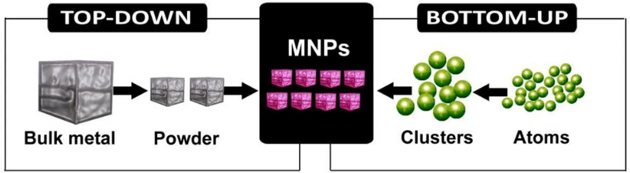
1.2.2 Synthesis: Top-down and Bottom-up approach
Nanomaterials can be fabricated either by using physical methods or chemical (wet) methods. Both methods can follow both Top-down approach that Bottom-up approach (Figure 1.5):
- Top down: the method consists in reaching nanometric dimensions, starting from a larger material. The massive material, "bulk," is divided into smaller particles, using mechanical energy, chemical or in other forms.
- Bottom up: the nanomaterial is obtained from the individual atoms, suitably assembled, by means of chemical reactions, allowing the precursor to increase with the size and the desired characteristics.
17
Figure 1.5:Top-down or Bottom-up approach
Both approaches can be conducted in a gas, in liquid, in fluids supercritical, solid or vacuum state. Most of the synthesis systems have as its central objective to control the size of the particles, their shape; the size distribution; the settlement; and the degree of agglomeration (in case colloidal systems). The control of these parameters is becoming increasingly necessary, in fact in the field of Nanotechnology the structure-property matching is enhanced, but is still unknown the potential of nanomaterials (Viau, G. et al., 2001).
1.3 New nanoheterogeneous systems: Nanocomposite
According to IUPAC definition, nanocomposite is “a composite in which at least one of the phases has at least one dimension of the order of nanometers” (Aleman, J. et al., 2007). In the broadest sense this definition comprises colloids, gels, porous media and copolymers, but usually it refers to the solid combination of a bulk matrix and a nanodimensional phase differing in structural and chemical properties. Natural structures are often comprised of and utilize nanocomposites, and scientific researchers commonly learn from the surrounding nature. In 1998, Oriakhi published a work entitled ‘Nano sandwiches’ (Oriakhi, C. O., 1998) stating “Nature is a master chemist with
18
incredible talent”. As a matter of fact, a number of biological arrangements are organized involving nanocomposite structures, thanks to ability of nature to conjugate, at nanometric level, organic and inorganic compounds, allowing the fabrication of smart materials with specific properties (mechanical, thermal, physical, electrical and/or chemical) and biological functions (e.g. biomineralization in diatoms, crustacean, mollusk shells, teeth and bones; inorganic catalytic activity in amino acids condensation (Mann, S., 1996) The resulting properties exhibited by these tiny materials can be noticeably different and unique from those of the substances with the same composition but in a larger size. In the 50s, the interest towards organic-inorganic composites increased due to their industrial applications in manufacturing paints (inorganic nanopigments suspended in organic mixtures), papers (cellulosic polymers cross-linked by metal oxo-species), coupling agents for glass, ceramics and metals modification (silanes, silicones, metallo-organics etc.). By the 1970s polymer/clay composites became a popular matter of discussion in textbooks, although the word "nanocomposites" had not been adopted, yet. In the early 1990s, an investigation onto a Nylon-6 loaded with a very small percentage of nanofillers, carried out by Toyota Central Research Laboratories, reported an evident improvement of mechanical and thermal features of the basic polymer, and pointed out that the properties of nanocomposite materials depended not only on the properties of their individual parents (nanofiller and nylon, in this case) but also on their morphology and interfacial characteristics. More recently, due to nanotechnology advance, polymer matrix-based nanocomposites have become a noticeable area of the research and development (Paul, D. R. et al., 2008; Sanchez, C. et al., 2005). Such materials, ranging between organic and inorganic chemistry, sounded highly versatile, offering a widespread range of possibilities to create customized materials both in terms of processing procedures and chemical and physical parameters (Sanchez, C. et al., 2004). Additionally, the fabrication of organized hybrid materials both within
19
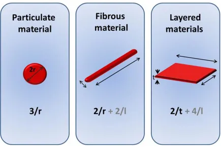
nanomicroscale and bulk materials plays a crucial role not only for academic research but overall for innovative industrial applications. Nowadays, new hybrid materials have been involved in a plethora of niche markets linked for instance to new generations of smart textiles, photovoltaic and fuel cells, antennas and satellite communications, optoelectronics, new catalysts and coatings, smart therapeutic vectors with controlled drug delivery properties, new ultra-sensitive sensors, cosmetics, smart papers, etc (Figure 1.6). The resulting nanoheterogeneous materials typically associate several aspects deriving not only from the mere sum of individual contributions but also related to the role of the inner interfaces, which could sometime be predominant. In the case of particles and fibres, the surface area per unit volume is inversely proportional to the material diameter; thus, the smaller the diameter, the greater the surface area per unit volume (Luo, J. J. et al., 2003). Common shapes of inorganic nanostructures when dispersed in a matrix (nanoparticles, nanotubes, nanofibres, fullerenes, and nanowires) and their respective surface area-to-volume ratios are reported in the (Figure 1.7).
20
Figure 1.7: Common shapes of inorganic nanostructures dispersed in a matrix (nanoparticles, nanofibres, nanowires) and their respective surface area-to-volume ratios.
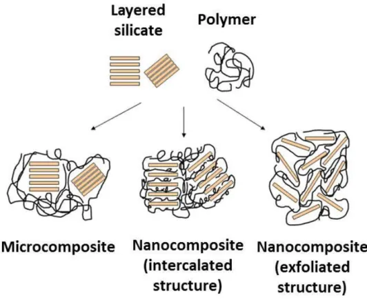
The properties of a nanocomposite are significantly influenced by the size scale of its component and phase, its ratio to the matrix phase and the degree of mixing between the two phases. Depending on the nature of components used and the method of preparation, significant differences in composite properties may be obtained. A typical example is reported in (Figure 1.8), where the classical diagram of the three types of arrangement of layered silicate materials within a polymer is depicted. When the polymer is unable to intercalate between the silicate sheets, a phase-separated composite is usually obtained, and the resulting properties are comparable to the traditional microcomposites (Alexandre, M. et al., 2000).
21
Figure 1.8: Classical diagram of the three types of arrangement of layered silicate materials within a polymer is depicted.
A better configuration is achieved when a single extended polymer chain can penetrate between the silicate layers (intercalated structure), forming a well-ordered multilayer morphology with alternating polymeric and inorganic layers. When the silicate layers are completely and uniformly dispersed in a continuous polymer matrix, an exfoliated or delaminated structure is achieved. In any case, the physical properties of the resultant composite are appreciably different. Likewise, in fibrous or particle-reinforced polymers, dispersion of the nanoparticle and their interaction with the matrix at the interface, play fundamental roles in determining the mechanical properties of the nanocomposite. Without proper dispersion, the nanomaterial will not provide any improvement in mechanical properties, when compared to conventional
composites. In addition, the properties of the overall nanocomposite can be
22
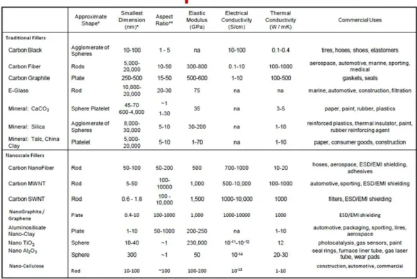
(e.g. a good adhesion improves interlaminar shear strength, delamination resistance, fatigue and corrosion resistance). Therefore, physical parameters like mobility and conformation of polymer chain and crystallinity degree were demonstrated to depend on the interface with the reinforcement into the bulk of the matrix (Ajayan, P. M. et al., 2003). A list of common nanoparticles and fillers is reported in (Figure 1.9). The introduction of small amounts of nanoparticles in matrices is expected to induce dramatic changes also in thermal, physical, electrical and chemical properties of the matrices themselves, depending on density and size parameters. Thus, particles with one dimension ≤5 nm, for example, tune catalytic activity, with ≤50 nm act on refractive index. More recently, a plethora of nanocomposite films consisting of either metal-metal oxide, mixed metal oxides, polymers mixed with metals or metal oxides, and carbon nanotubes mixed with polymers, metals or metal oxides have been synthesized and investigated for their application as active materials for sensors (Dongfang, Y., 2001). Design of the nanocomposite films for gas sensor applications requires that many factors are taken into account, such as the surface area, interfacial characteristics, electrical conductivity, nanocrystallite size, surface and interfacial energy, stress and strain, etc., all of which depending significantly on the material selection, deposition process methods and parameters. Finally, in addition to nanocomposite thin layer fabrication, nanocomposite polymer fibres (nanoparticles dispersed within single nanofibres) have aroused great interest among academic disciplines and industrial sectors for their huge potentials and intriguing applications into smart textiles, cell scaffolding, drug delivery, filtering, sensing and biosensing.
23
Figure 1.9: A list of common nanoparticles and fillers
1.3.1 Nanocomposite thin film fabrication methods
Traditional synthesis approaches for manufacturing nanophased composite materials at the solid state can be grouped into four strategies, such as melt
intercalation (co-extrusion), functionalization of the NPs, in-situ
polymerization and surfactant assisted dispersion, respectively. An accurate description of these approaches is reported in literature (Mittal, V., 2012). As far as sensor construction is concerned, a chemical layer should be placed on a suitable transducer or substrate. Several technologies allow nanocomposite thin film depositions (up to a few micrometers) on several substrates through a variety of methods such as physical vapor deposition (PVD), chemical vapor
24
deposition (CVD) and wet chemical processes (i.e. sol-gel and electrochemical deposition, thermolysis, flame spray pyrolysis, etc.). The kind of deposition technique used strongly affects the properties of the composite layer. To fabricate heterogeneous films consisting of materials with very different nature, e.g. a metal or a metal oxide with a polymer is obviously much more challenging than to deposit films comprised only of a single type of material. Such a deposition process should be able to vaporize or alloy materials of different nature onto the same substrate at the same time. Within this section the most common deposition methods used to fabricate nanocomposite films for gas sensing will be summarized.
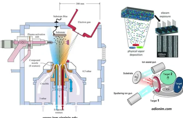
1.3.1.1 Physical Vapor Deposition
PVD involves only physical processes, such as high temperature vacuum evaporation, using electron beam, plasma sputtering, resistance heating and pulsed laser deposition under vacuum. The deposition of a thin film commonly occurs by condensation of the vaporized form of materials onto various substrate surfaces. To obtain a nanocomposite film the energy sources have to be able to vaporize all the component materials under the same processing parameters (i.e. vacuum levels, temperature etc.) and simultaneously condense them onto the same substrate. Sputtering, which is one of the PVD processes, occurs whenever any particle strikes a surface with enough energy to dislodge an atom from the surface, with a yield resulting from the ratio of the number of emitted particles per incident particle:
Y=Nemitted particles/Nincident particles
Sputter deposition is achievable whatever the incident species, including atoms, ions, electrons, photons and neutrons as well as molecules and
25
molecular ions. The yield for bombardment of a surface with an ion or an atom of the same energy will be practically identical; physical sputtering relies on the transfer of physical momentum and kinetic energy from the incident particle to the surface atoms, and this is independent from the particle charge (Figure 1.10).
Figure 1.10: A typical PVD apparatus used to deposit nanocomposite films.
A gas sputtering, such as argon or nitrogen, impacting composite material sources (targets consisting of pre-mixed compounds or a few targets simultaneously sputtered by ions) is able to deposit a composite thin film (mixture of metal oxides, a metal together with a metal oxide, or a metal and a polymer). Another PVD process that usually used to deposit nanocomposite films is pulsed laser deposition (PLD) (Douglas, B. et al., 1994),where a high power pulsed laser beam inside a vacuum chamber is focused to strike a target of the material that needs to be deposited. This material is vaporized from the target (in a plasma plume) and deposits as a thin film on a substrate facing the
26
target. This process can occur in ultra-high vacuum or in the presence of a background gas, such as oxygen that is commonly used for depositing oxides to fully oxygenate films. The process of PLD can generally be divided into four main steps:
1. laser ablation of the target material and creation of a plasma; 2. dynamic of the plasma;
3. deposition of the ablation material on the substrate;
4. nucleation and growth of the film on the substrate surface.
All steps are essential for the uniformity, crystallinity and stoichiometry of the resulting layer. The ablation of the target material upon laser irradiation and the creation of plasma are very complex processes. The removal of atoms from the bulk material is obtained by vaporization of the bulk at the surface region in a state of non-equilibrium. During this process the incident laser pulse penetrates into the surface of the material until a depth dependent on the laser wavelength and the index of refraction of the target material at the applied laser wavelength. Typical values of such a depth for most materials are in the region of 10 nm. The strong electrical field generated by the laser light is sufficiently strong to remove the electrons from the bulk material within the penetrated volume. The free electrons oscillate within the electromagnetic field of the laser light and can collide with the atoms of the bulk material, thus transferring part of their energy to the lattice of the target material within the surface region. The surface of the target is then heated up and the material goes finally into the vapor form. In the plasma dynamic step, the material expands in a plasma, parallel to the normal vector of the target surface and towards the substrate, due to Coulomb repulsion, and recoil from the target surface. The third step, i.e. deposition on the substrate, determines the quality of the deposited films by triggering nucleation and growth of films on the substrate surface. Finally, the nucleation depends on several growth
27
parameters, including laser energy, surface temperature and structure of the surface substrate, gas pressure. Since PLD source does not interact with the gas phase species and it is very easy to manipulate, the dynamic range of deposition pressures is the largest, when compared to other vacuum deposition processes. In addition, since typical laser wavelengths used in PLD process are less than 250 nm, any material can be virtually laser evaporated, within such a short wavelength, then allowing to deposit composite films consisting of a variety of materials. Therefore, nanocomposite thin film can be easily fabricated through PLD when a target consists of a powder of pre-mixed source materials or when multiple targets of different materials are ablated simultaneously. The ability of the technique to reproduce the target composition is a unique feature to control the composition of nanocomposite films. Another PVD process suitable to get nanocomposite layers is the high temperature vacuum evaporation: it works heating the material (by an electrically resistive heater or electron beam) until evaporation at low pressure (less than 10-5 torr) and condensing it onto a substrate by a flux of vapor. The material to vaporize is typically heated until its vapor pressure is high enough to produce a flux of several Ångströms per second. In order to deposit nanocomposite films, powders of two or more materials may be mixed and compressed into pellets usable for evaporation. It is also possible to evaporate different materials using multiple heating sources. In this case, each time of flight can be ruled separately by increasing or decreasing the power of the heating source. Vacuum evaporation is very useful to fabricate nanoheterogeneous thin films due to ease to obtain uniform mixing over a wide range of concentrations.
28
1.3.1.2 Chemical Vapor Deposition
Chemical vapor deposition (CVD) is a chemical process often used in the semiconductor industry to produce thin films. The substrate is exposed to more than one volatile precursor reacting and/or decomposing on the substrate surface to produce the desired composite films in various forms, including mono- and polycrystalline, amorphous and epitaxial. However, only recently CVD process has been used to produce nanocomposite films for gas sensor applications (Russel, B. et al., 2011). The methodologies are based on the incorporation of an aerosol into the process, essentially the use of a liquid-gas aerosol to transport precursors to a heated substrate. The use of an aerosol allows to carry preformed nanoparticles, these may be incorporated into a conventional CVD flow (hybrid CVD) or transported with another semiconductor precursor (aerosol assisted CVD or AACVD). The main benefit of this technique is its great flexibility since many preformed nanoparticle solutions can be used, and combined with any chemically compatible precursor, to fabricate a huge variety of nanoheterogeneous layers. In addition, it comprises a relatively simple one-step process without special handling steps. Flame spray pyrolysis (Madler, L. et al., 2002) is a one-step combustion process of solution precursors able to get nanocomposite materials of mixed oxides. The precursors can be directly solved in the solvent (e.g. ethanol, iso-octane or methanol), and then introduced into the hot reaction zone (e.g. a flame) (Tani, T. et al., 2000), for a high-velocity spray jet for rapid quenching of aerosol formation. The particles sizes usually range 1-500 nm, depending on the process parameters, with production rates up to 250 g/h.
29
1.3.1.3 Wet-chemical deposition
The sol-gel process is a wet-chemical technique (chemical solution deposition) that is extensively used to fabricate nanocomposite layers, even on very large surface areas. Primarily, such methods are used for the deposition of materials (usually metal oxides) starting from a colloidal solution (sol) acting as the precursor for an integrated network (or gel) of either discrete particles or network polymers. Typical precursors are metal alkoxides and metal salts (such as chlorides, nitrates and acetates), which undergo hydrolysis and polycondensation reactions. During the process, a sol (or solution) containing sources for component materials (such as metal alkoxides and metal chlorides
precursors for metal oxides, metallic nanoparticles for metals,
tetraethoxysilane for silica matrix, catalyzers, stabilizers and other additives for porosity generation) is arranged first. The sol then undergoes hydrolysis and polycondensation reactions, gradually evolving towards the formation of a gel-like network containing both a liquid and a solid phase. The basic structure of the solid phase can range from discrete colloidal particles to continuous chain-like polymer networks. The main deposition techniques to create the precursor layer on a substrate are dip coating (Brinker, C. J. et al., 1997) spin coating (Vorotilov, K. et al., 1995) or casting. In the first deposition technique, the substrate is normally withdrawn vertically from a coating solution: the film results from a complex process involving gravitational draining with concurrent drying and continued condensation reactions. Therefore, a substrate is removed from the solution at a defined withdrawal speed under controlled environmental conditions (temperature, humidity and air flow). The formation of thin films occurs through solvents evaporation (mainly ethanol and water), which concentrates non-volatile species in the system, then leading to aggregation and gelation. The resulting layer depends on size and structure of precursors, relative rates of condensation and
30
evaporation, capillary pressure, substrate surface and withdrawal speed. Specifically, film thickness is mainly controlled by withdrawal speed, non-volatile species content and solution viscosity. It is the oldest and the most widely used deposition technique in industry probably due to its ease of use, its cost efficiency, high coating quality and its flexibility (Aegerter, M. A. et al., 2004). In spin coating, few drops of a desired liquid are put onto the substrate held in place using a rotatable fixture; then, spinning is accelerated until high angular velocities in order to spread out the fluid by centrifugal force leaving a thin uniform film. This technique involves the equilibrium between the centrifugal forces and the viscosity of the solution: thickness and homogeneity depend on the rotational speed, the content of non-volatile species in the sol and the volatility of the liquid. Such technique is not expensive and is reproducible, simple and able to coat different smooth and flat substrates. Further steps to fabricate nanocomposite films are comprised of decomposition and pyrolysis of organic compounds, water and residual organics elimination and crystallites nucleation and growth as a network. Specifically, the process uses inorganic or metal organic compounds as raw ingredients diluted in aqueous or organic solvents. Such substrates are hydrolyzed and condensed to form inorganic polymers characterized by O M bonds. In the case of inorganic compounds, hydrolysis proceeds through a
proton removal from an aquo ion [MONH2N]2+ to form a hydroxo O or
oxo O ligand. Then, condensation reactions involving the hydroxyl ligands create O bonds with water removal. The thermal decomposition behavior of the gel precursor plays an important role in crystallites size and in film porosity: it is often necessary to favor a further polycondensation and enhance mechanical properties and structural stability via final sintering, densification and grain growth. Therefore, sol-gel sounds like an excellent technique for preparing high purity multicomponent films. Even small quantities of dopants can be introduced in the sol and end up dispersing uniformly in the final product. Great scientific interest is focused on this
31
relatively simple and not expensive strategy to fabricate heterogeneous systems. For instance, Choi et al. (Choi, Y. J. et al., 2011) fabricated nanocomposite layers of polystyrene with a self-assembled layer of gold nanoparticles (d=18-22 nm), synthesized directly via aminosilane, with distance between nanoparticles controllable via a sol–gel reaction. Ponemareva et al. (Ponemareva, A. A. et al., 2012) prepared nanocomposite
SiO2-SnO2 thin films on oxidized silicon substrates using the sol-gel technique
mixing SnCl2·2H2O. Finally, other wet coating techniques can be used to
fabricate a thin film such as spray coating (Langlet, M. et al., 1994), ink-jet printing (Emine, T. et al., 2008) doctor blading (Pitchunami, R. et al., 1995) and capillary or meniscus coating (Belleville, P. F. et al., 1994), all of which depending on the area and the quality of the surface to be deposited. Spray technique is suitable for fast coating of irregular surfaces: very fine droplets are ejected from the solution using nebulizers or atomizers and are then driven by a gas carrier onto a substrate. Ink-jet deposition is commonly used for nanotechnologies, organic electronics and tissue engineering due to its ability to precisely deposit picoliter volumes of solutions or suspensions in well-defined patterns. Doctor blading, commonly used for coating large substrates, is able to produce thin films with a well-defined thickness by placing a linearly moving sharp blade at a fixed distance from the substrate surface to coat, then leaving a thin wet film. Capillary or meniscus technique is capable of coating flat substrates at room temperature with a very high uniformity of the thickness: the deposition comprises a substrate that is taken under vacuum onto a chuck, while a tubular dispense unit gradually is moved ensuring a continuous solution feed. No physical contact occurs during the deposition travel, but the narrow gap between substrate and applicator allows the formation of a spontaneous meniscus.
32
1.3.1.4 Electrospinning:one-dimensional composite
nanomaterials creation
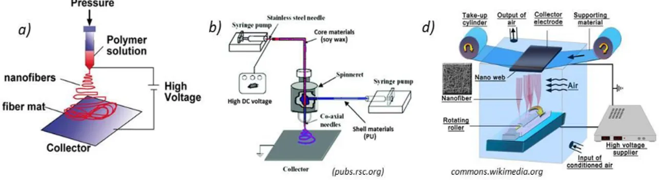
Among a series of advanced techniques developed to create 1D nanostructures with well-controlled morphology and chemical composition, Electrospinning sounds to be the most versatile technique capable of generating, even in a single step, composite nanostructures from a great assortment of polymers. Such a technique is a variation of the electrospray process where liquid drops are elongated with the increasing of the electric field, until generating micro-nanofibrous structures (Joachim, H. et al., 2012). This technique is discussed in detail in the following chapter.
1.4 Characterization techniques
Characterization tools are decisive to comprehend the physical and chemical basic properties of nanocomposites. Depending on the final application, it facilitates the study of emerging materials by providing information about some intrinsic properties. The nanocomposite materials can be analyzed and tested in relation to six main different aspects: mechanical, thermal, chemical, physical, morphological and electrical properties. Therefore in this paragraph are described various techniques of characterization performed on studied and designed nanocomposites which will be described in the following chapters.
33
1.4.1 Morphological characterization
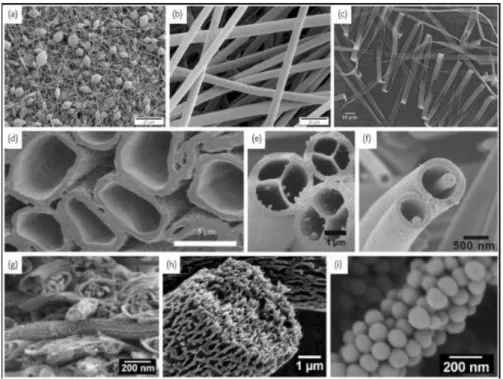
Nanocomposites morphology deals with all the structure of systems, mostly in solid state. For instance, nanostructured materials morphology is studied because of the strong relationship occurring between morphology and properties. Indeed, morphological characterization can supply a lot of information, mostly about the structure of homopolymers, copolymers, polymer blends and the size, shape and dispersion of micro- and nanocompound within a matrix. For morphological characterization of our nanocomposites have been used some advanced microscopic techniques: Scanning Electron Microscopy (SEM), Transmission Electron Microscopy (TEM), high-resolution transmission electron microscopy (HRTEM) and Atomic Force Microscopy (AFM).
Scanning Electron Microscopy (SEM): in nanotechnology, Scanning Electron Microscopy is the most common technique to investigate the morphology of thin films or fibers (or other nanostructures) with and without nanofillers, since it is like a photograph of the sample at a very high magnification (up to 2000000X) and high resolution (up to 0.5 nm). Thus it depict a 3D-like structure of the surface, enhancing the roughness, fractures, clusters, composite dispersion and all the relevant information related to the topography of a nanocomposite (shape, size and positions of particles). The Scanning Electron Microscope (SEM) is a microscope that uses electrons instead of light to form an image. A beam of electrons is produced at the top of the microscope by an electron gun. The electron beam follows a vertical path through the microscope, which is held within a vacuum. The beam travels through electromagnetic fields and lenses, which focus the beam down toward the sample. Once the beam hits the sample, electrons and X-rays are ejected from the sample. Detectors collect these X-rays, backscattered electrons, and secondary electrons and convert them into a signal that is forwarded to and
34
displayed on a monitor (presently a computer monitor) as final image. All metals are conductive and require no preparation before being used. Generally, all non-metals matters need to be made conductive by covering the sample with a thin layer of conductive material (such as gold) by a "sputter coater." Non-conductive specimens, in fact, tend to charge when scanned by the electron beam, especially in the secondary electron imaging mode. This can cause scanning faults and other image artifacts. SEM provides then images concerning surface features associated with a sample. Therefore, SEM micrographs can reveal the surface morphological changes caused by the nanofillers within the thin matrix. However, there are two other well-known branches of microscopy, Scanning Probe Microscopy and Scanning Tunnelling Microscope, which are very useful in nanotube research. In Scanning Probe Microscopy, a physical probe inside a specific microscope (SPM), commonly a sharp tip, scans the sample surface in order to obtain an image from the interactions occurring between the tip and the specimen, as a function of position. In Scanning Tunnelling Microscopy, instead, a sharp conducting tip inside a specific microscope (STM) is held sufficiently close to a surface (typically about 0.5 nm), such that electrons can ‘tunnel’ across the gap. This method provides surface structural and electronic information at atomic level.
Transmission Electron Microscopy (TEM): Recently, several studies have been conducted to investigate the behavior of polymer-based nanocomposites. In contrast to SEM, which scans a surface to produce its image, in the specific microscope fabricated according to Transmission Electron Microscopy principles (TEM), the electron beam is transmitted through an ultra-thin sample to observe the density of its constituents and thus producing an image through density variations: electrons penetrate and cross to the opposite side of the sample producing a projected image on a phosphor or fluorescent screen, or more recently on a computer monitor after the sensor detection of a CCD camera. TEMs use electrons as “light source” and their much lower