FACOLTÀ DI INGEGNERIA
DIPARTIMENTO DI INGEGNERIA ELETTRICA ELETTRONICA E INFORMATICA
ANNO ACCADEMICO 2010 - 2011
Dottorato di Ricerca in Ingegneria Elettronica Automatica e del
Controllo dei Sistemi Complessi
XXIV Ciclo
GIUSEPPE PAPOTTO
BATTERYLESS RF TRANSCEIVER FOR
WIRELESS SENSOR NETWORKS
Ph.D. Thesis
Tutor:
Chiar.mo Prof. G. PALMISANO Coordinatore:
Acknowledgements... iv
Abstract... v
Chapter Ι: RF-powered transceivers for WSNs... 1
1.1 Wireless sensor networks ... 3
1.1.1 Applications ... 5
1.2 Energy harvesting systems... 8
1.3 RF-powered sensor networks ... 11
1.3.1 Frequency bands ... 12
1.3.2 Data rate ... 13
1.3.3 Operating range ... 14
1.4 RF-powered transceiver ... 15
1.4.1 Proposed solution ... 17
Chapter IΙ: Batteryless RF transceiver design... 19
2.1 RF harvesting module ... 20
2.1.1 Multi-stage rectifiers for RF harvesting systems ... 22
2.1.2 Threshold self-compensated rectifier ... 28
2.1.4 Design of the matching network ... 35
2.1.5 Design of the rectifier... 38
2.1.6 Harvester simulated performance... 44
2.2 Power management unit... 44
2.2.1 Voltage reference ... 47
2.2.2 Hysteresis comparator ... 52
2.2.3 Voltage regulator... 54
2.2.4 Voltage limiter... 55
2.2.5 Power management unit simulated performance ... 56
2.3 RF front-end... 58
2.3.1 Limiter... 61
2.3.2 Frequency dividers ... 63
2.3.3 Phase frequency detector and charge pump ... 66
2.3.4 Voltage controlled oscillator ... 70
2.3.5 Loop filter... 75
2.3.6 Output buffer ... 75
2.3.7 RF front-end simulated performance ... 76
Chapter III: Experimental results... 81
3.1 RF harvester stand-alone... 82
3.2 Batteryless transceiver ... 89
3.2.1 Power management unit characterization ... 91
3.2.2 RF front-end characterization... 95
Conclusions ... 109 Appendix ... 112 References ... 119
I would like to thank Professor Giuseppe Palmisano, for his scientific guidance and support during these years. I am very grateful to Eng. Francesco Carrara, for his technical advice and collaboration in carrying out this work. I was very pleased to work with him. I thank Eng. Alessandro Finocchiaro for his contribution to this project. I would also express my appreciation to Alessandro Castorina, Santo Leotta and Egidio De Giorgi. Without their help and technical expertise, the experimental characterization of the designed circuits would have been more difficult. I’m very grateful to my colleagues at RFADC. They have been a constant source of helpful discussions and distractions.
Finally, I’m deeply thankful to my family for their support and encouragement over these years.
Wireless sensor network (WSN) is a fast growing research area which has attracted considerable attentions both in industrial and academic environments in the last few years. The recent technological advances in the development of low-cost sensor devices, equipped with wireless communication interfaces, open up several applications in different fields. Prototypes exist for applications such as early detection of factory equipment failure, optimization of building energy use, structural integrity monitoring, etc. Other addressable market segments are healthcare, home automation, automotive and radio frequency identification (RFID).
However, some barriers to widespread adoption of WSNs still remain. The most critical issue is related to the extension of the battery lifetime of sensor nodes. Indeed, conventional wireless platforms rely on internal batteries, which suffer from a limited lifetime. On the other hand, in typical WSN application scenarios, periodical battery replacement is impractical because of either the large number of deployed devices or inaccessible node placement (e.g. implanted in human body or embedded into the structures to be monitored). The need for low-cost hardware is a critical issue as well, since it affects the overall network costs. This work is aimed at drastically facing these critical issues by recourse to an innovative node concept, which is quite different from traditional architecture approaches.
In particular, in this work a RF transceiver is presented, which is conveniently lacking both the battery and the frequency synthesizer (commonly adopted to provide the LO signal to the RX and TX sections of the front-end).
Battery-less operation is achieved by recourse to a RF energy harvesting system. It allows the nodes to collect the needed supply power from the RF carrier transmitted by a network hub, which also acts as a gateway for the data stream. Such solution radically solves the battery-lifetime problem, since RF-powered devices are ideally free of maintenance. Moreover, as above mentioned, the use of the frequency synthesizer is avoided as well. Such target is achieved by adopting a PLL-based RF front-end. Indeed, the RX section of the designed front-end is able both to recover incoming data and synthesize the TX carrier from the input RF signal. Incidentally, the adopted front-end architecture enables sparing the quartz resonator which is normally exploited as a frequency reference. This results in an highly integrated and low-complexity/low-cost transceiver solution, which is particularly suitable for WSN applications.
This dissertation is organized as follows. In chapter I, after a brief overview about WSNs and their applications, the system architecture is presented and discussed. A prototype of the proposed RF transceiver was designed and manufactured in a 90-nm CMOS technology by TSMC. The IC design is discussed in chapter II, while experimental results are reported in chapter III, then conclusions are drawn.
This project was carried out within the RFADC (Radio Frequency Advanced Design Center), a joint research group supported by the University of Catania and STMicroelectronics.
RF-powered transceivers for
WSNs
A sensor is a device which is able to convert a physical quantity into an electrical signal. This signal may be passed to a measurement or processing system for storage and analysis, or used as input to some controlled process. Sensors integrated into structures, machines and the environment, coupled with an efficient delivery system of the sensed data, could provide great benefits in several application fields [1]. Several market segments can be potentially covered, including safety, environmental and structural monitoring, healthcare, radio frequency identification (RFID), automotive, home automation, etc. However, some barriers to widespread use of sensors still remain. The deployment of wired sensor networks entails significant and long term maintenance costs, limiting the number of sensors that may be deployed, thus reducing the overall system quality. On the other hand, the adoption of a wireless communication interface allows lowering the deployment costs, but the maintenance issue remains.
Indeed, sensor nodes of a wireless sensor network (WSN) typically rely on internal batteries for their operation. Unfortunately, batteries suffer from a limited lifetime, thus they need to be periodically replaced. The extension of the battery lifetime is the most critical challenge concerning the implementation of WSNs. This issue is even more crucial for all those scenarios in which periodical node battery replacement is impractical because of either a large number of devices or inaccessible node placement.
Recently several works have been addressed to the development of
autonomous sensor nodes, which are able to derive the energy needed for their operation from the environment by exploiting an energy harvesting system [2]-[5]. The greatest innovation of these devices lies in the battery-free operation which enables applications that would be prohibitively expensive due to the maintenance costs. The implementation of autonomous WSNs requires both the minimization of the power consumption of the node hardware, by means of ultra-low power IC design, and the adoption of proper power management strategies. The most power-hungry component of a sensor node is its wireless interface. Therefore, designing low-power low-complexity transceivers is the main challenge concerning the implementation of autonomous WSNs.
This dissertation deals with the design and characterization of a battery-less transceiver for WSN applications, which includes a RF energy harvesting module, a power management unit and an ultra-low power RF front-end. In this chapter, the design challenges are discussed along with the related state-of-art solutions. Finally, the proposed solution is presented and discussed.
1.1
Wireless sensor networks
A wireless sensor network generally consists of a base station (or “gateway”) which is able to communicate with a number of wireless sensors via a radio link. Data is collected at the sensor node and transmitted to the gateway. The transmitted data are then processed by the system. A block diagram of a wireless sensor node is shown in Fig. 1.1.
Fig. 1.1. Block diagram of a wireless sensor node.
A modular design approach is usually adopted in order to provide a flexible and versatile platform which is able to address the needs of different applications. For instance, the conditioning circuit may be programmed or replaced according to the sensing unit. The use of a memory unit allows the node to acquire data on command from the base station or when an event happens. The system is also
equipped with a microcontroller, whose main task is to manage the communication protocol.
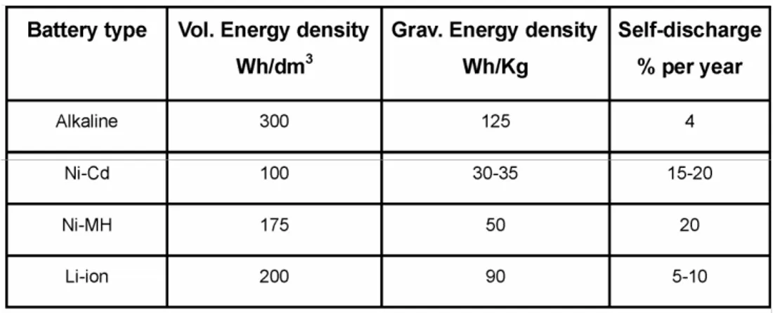
A key issue concerning the design of a wireless sensor node is to minimize its power consumption. Generally, the radio subsystem requires the largest amount of power. Thus, it is advantageous to transmit data only when needed. Accordingly, a duty-cycled operation of the RF front-end is usually implemented. As regard the node power supply, it is worth nothing that, today batteries represent the dominant energy source. Thanks to the advances in battery technology, their energy density with respect to volume and weight (volumetric and gravimetric energy density) has increased by a factor of three in the past 15 years [6][7]. Table 1.1 shows some typical values of energy densities and self-discharge values for commercial batteries.
Table 1.1. Characteristic of batteries.
Nevertheless, battery lifetime is a crucial issue which has up to now limited the widespread adoption of WSNs, in which there are usually dozens or hundreds of small devices to power up. To overcome such limitation, alternative solutions to batteries have been investigated. One possibility is to replace them with energy
storage systems featuring larger energy density. Concerning this, one promising technology is miniaturized fuel cells [8]. Basically, a fuel cell is a power generator that use chemical fuels (i.e. hydrogen or methanol). The gravimetric energy density of these systems is expected to be three to five times larger than Li-ion batteries. However, the maintenance issue is not solved since these cells need to be refuelled.
Recently the power supply issue has been faced by recourse to energy harvesting systems, which are able to collect the needed power from the environment (e.g. from vibrational energy, thermal energy, solar energy or RF radiation). This energy is stored in a capacitor and used to supply the whole system. Such approach enables battery-free operation allowing the deployment of potentially maintenance-free wireless sensor networks.
1.1.1
Applications
Wireless sensor network is an emerging technology with a great potential. The ability to add remote sensing points, without the cost of running wires, results in numerous benefits including energy and material savings. Several application fields may benefit from WSNs. For instance, wireless sensor network is a promising technology for medical applications. Recent years have seen the multiplication of body sensor network platforms, and a number of wireless sensor nodes for the monitoring of various biological and physiological signals ca be found [9]. These sensor nodes differ by form factor, autonomy, and their building blocks, but they all face the same technological challenges such as autonomy,
A leading sector concerning the development of wireless sensor networks is the automotive one. More and more sensors will be placed in the future cars. Tire pressure monitoring systems (TPMSs) are examples of WSNs used for safety [10]. Today such systems are powered by relatively large batteries, which limit both data transmission frequency and the system lifetime.
Fig. 1.2. Tire pressure monitoring system.
To overcome such limitations, the next-generation TPMS should be powered by energy harvesting systems. Structural monitoring is another important application field of WSNs. Sensors embedded into machines and structures enable condition-based maintenance of these assets. Typically, structures or machines are inspected at regular time intervals, and components are repaired or replaced based on their hours in service or on their working conditions. However, this approach is expensive if the components are in good working order or if a damage occurs
between two inspection intervals. Thanks to wireless sensing assets may be inspected when it is needed, reducing maintenance costs and preventing possible catastrophic failures. As regards the structural monitoring, one of the most recent applications of WSNs is related to the monitoring of large civil infrastructures, such us the Ben Franklin Bridge (Fig. 1.3).
Fig. 1.3. Ben Franklin Bridge.
The strain suffered by this structure is monitored by a network of wireless sensors powered by lithium batteries, which are able to provide more than one year of continuous operation [1].
Other application fields are home automation (WSNs are keys building blocks for smart homes), environmental monitoring (random deployment on large-scale areas makes monitoring of agriculture easier) industrial automation (WSNs may replace traditional cabling in monitoring and control systems), assets tracking (radio frequency identification tags may be placed onto or into objects
and products to perform remote identification and tracking by means of radio waves) [11].
1.2
Energy harvesting systems
Energy harvesting systems can be grouped into three categories according to the type of energy they use, which may be kinetic, thermal or electromagnetic energy (including both solar and RF radiation).
Kinetic energy is converted to electrical energy by exploiting the displacement of a moving part or the mechanical deformation of some structures inside the energy harvesting module. For converting this displacement or deformation the established transduction mechanisms are electrostatic, piezoelectric or electromagnetic. In electrostatic transducers, the distance or overlap of two electrodes of a polarized capacitor changes due to the movement or the vibration of a movable electrode. This motion produces a voltage change across the capacitor and results in a current flow in an external circuit. In piezoelectric transducers, vibrations cause the deformation of a piezoelectric structure, which generates a voltage proportional to the applied strain. In electromagnetic transducers, the relative motion of a magnetic mass with respect to a coil causes a change in the magnetic flux that generates an AC voltage across the coil [12]. For a given vibrational energy source, the highest power output is achieved by piezoelectric conversion. Recent advances in MEMS technology allow piezoelectric-based energy harvesting systems to be miniaturized (Fig. 1.4) opening up their adoption by WSNs [13][14].
Fig. 1.4. Schematic of a piezoelectric micro-power generator [14].
However, such systems, which are particularly suitable in industrial environments (where a large amount of vibrational energy is present), may prove ineffective for other applications, such as home automation or structural and environmental monitoring. Thermal energy harvesting devices may use the thermal energy coming from different environmental sources: persons, animals, machines. A thermoelectric generator basically consists of a thermocouple, comprising a p-type and n-type semiconductor connected electrically in series and thermally in parallel. The thermogenerator (based on the Seebeck effect) provides an electrical current proportional to the temperature difference between its hot and cold junctions. An electrical load is then connected in series with the thermogenerator creating an electric circuit [12]. The most widely used material
Bi2Te3. Poly-SiGe has also been used, especially for micro-machined thermopiles
[15]. Moreover, research on nano-structured materials is ongoing worldwide in order to optimize thermoelectric generator performance.
Fig. 1.5. Micro-machined thermopile [15].
Another energy source which is profitably used to perform energy harvesting is the electromagnetic radiation, either in the form of light (known as solar energy), or lower frequency RF radiation. Both methods are extensively used in many present devices.
Solar energy is a mature technology. Photovoltaic systems are found from the megawatt to the milliwatt range producing electricity for a wide range of applications. Outdoor they are a viable energy source for self-powered systems. Indoor the illumination levels are much lower (10-100 µW/cm2), which requires a fine-tuning of the cell design to the different spectral composition of the light and the lower level of illumination. The described energy harvesting systems share the
common limitation of being reliant on ambient sources generally beyond their control.
RF energy harvesting systems overcome such limitation [16]. Indeed, RF power can be easily provided when needed, in every location. To this aim, RF harvesting systems rely on a RFID-like approach, in which power is delivered to passive tags through the radio waves transmitted by a reader. This solution gives great flexibility to the system. RF-powered devices can be located in inaccessible or hazardous areas, or locations where battery replacement is highly impractical. For this reason, a RF-powered approach was chosen as the best solution for the design of a battery-free transceiver for wireless sensor network applications. A description of the main features of a RF-powered sensor network is provided in the next section.
1.3
RF-powered sensor networks
RF-powered devices provide an enabling technology for the deployment of low-cost wireless sensor networks. Such devices rely on the extraction of energy from propagating radio waves instead of internal power sources. Today, RF-powered devices are widely used in passive radio frequency identification (RFID) systems. Furthermore, many biomedical implanted equipments exploit radio waves to extend their lifetime. Possible applications also include telemetry systems, structural monitoring, and home automation. As shown in Fig. 1.6 RF-powered sensor network architectures rely on the use of a central hub, which is able to provide the nodes with both the needed supply power and the reference
frequency through a RF carrier, besides operating as a gateway for the data stream.
Fig. 1.6. RF-powered sensor network.
Adopting such network concept radically solves the problem of battery lifetime, since RF-powered nodes are ideally free of maintenance.
1.3.1
Frequency bands
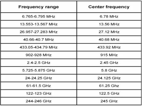
Low-power RF devices, such as wireless sensor nodes, usually operate within unlicensed bands, which are often referred to as ISM bands. These are portions of the frequency spectrum reserved internationally for the use of radio frequency waves for industrial, scientific and medical purposes. Unlicensed means that the user of these products doesn’t need for an individual license from the telecommunication regulatory authorities, but it doesn’t mean unregulated. On the contrary, wireless devices need to meet strict regulations on the operating frequencies, output power, spurious emissions, among other things.The ISM
bands are defined by the ITU-R (International Telecommunication Union Radiocommunication Sector), which is responsible for the development of standards for radio-communication systems. The designed bands are listed in Table 1.2 [17].
Table 1.2. ISM frequency bands.
The individual countries’ use of these bands may differ due to variations in national radio regulations.
1.3.2
Data rate
The communication requirements of WSNs are quite different from those of traditional wireless links. For instance, in WLAN networks, data are transmitted at a rate as high as possible. Similarly, in mobile phone networks, data rate must be high enough to ensure a good quality of service (QoS). In contrast, in WSNs, data
To this aim, duty-cycled operation schemes are usually adopted at the node level in order to reduce as much as possible the use of the wireless interface, which is the most power-hungry component of a wireless sensor node. Moreover, an investigation of the data flow in WSNs reveals that the operation of wireless sensor nodes is usually event-driven, namely data transmission occurs only when the monitored physical quantity changes or a request from the hub is received. On the other hand, in most application scenarios, slowly variable phenomena are monitored. Therefore, each node transmits a few packets/second. Moreover these packets are relatively short (typically less than 200 bits/packet). As a result, the average data rate of each wireless sensor node usually doesn’t exceed 1 Kbps [18].
1.3.3
Operating range
A key parameter of a wireless sensor network is the operating range, i.e. the maximum allowed distance between the hub and the sensor node. In most application scenarios an operating range of about 10 m is required.
In a RF-powered sensor network, two conditions must be fulfilled to ensure communication between the hub and each sensor node. First, the available input power at the antenna connector of the node must be sufficient to guarantee proper operation of its equipment. As a matter of fact, RF-powered devices rely on the extraction of the needed DC power from the radio waves transmitted by the hub. Furthermore, the signal transmitted by the node must be sufficiently strong when it reaches the hub, so that it can be received without errors. Traditionally, RF-powered devices (such as. passive RFID tags) are downlink (hub to node path)
limited, namely the system operating range is limited by the power that the device can harvest from the radio waves transmitted by the hub. However, such systems use a backscattering-based transmission scheme for the uplink communication (from node to hub). According to this approach, sensor nodes should transmit data to the hub in a passive way, by simply reflecting the incident RF power coming from the hub. In this case, the hub sensitivity plays an important role in the definition of the system operating range [19]. Indeed, in a RF-powered network architecture, the transmitter of the hub must be permanently on to ensure proper operation of the network nodes. Therefore, it induces a significant amount of noise to the receiver input of the hub itself, lowering the signal to noise ratio (SNR). This problem, which is referred to as self-jamming, is even more relevant considering that the backscattered signal lies in the same band of the signal transmitted by the hub. In this case, the node’s signal should lie no more than 100 dB below the level of the hub’s carrier signal to be correctly received [20]. As increasingly efficient RF energy harvesting systems are being introduced, the downlink operating range progressively extends and the uplink power budget turns out to be the bottleneck of the backscattering-based systems.
1.4
RF-powered transceiver
The main challenge in the implementation of a RF-powered sensor network is to design an ultra-low power RF transceiver, which is able both to efficiently harvest the power needed for the node operation and to perform the communication task. Several works have been reported in literature about this
topic. A first proposed approach basically relies on a RFID-like platform equipped with an ASK demodulator and a backscattering-based transmitter [21][22]. Such solution ensures low power consumption, since most part of the system is passive. Combining low-power ICs with improved RF energy harvesting systems allows extending the downlink operating range. On the other hand, as above explained, backscattering-based systems suffer from the hub self-jamming, which limits the uplink operating range.
To overcome such limitation, RF-powered transceivers have been proposed which exploit an active transmission scheme. RF-powered transceivers equipped with UWB transmitters are presented in [23]-[25]. These devices are remotely powered through an UHF signal, which is also used to perform the downlink communication. Conversely, an UWB transmission scheme is used for the uplink communication with the aim of achieving both high data rates and low current consumption through very simple (crystal-less) circuit architectures at the sensor node side. However, adopting an UWB transmission approach considerably challenges the receiver section of the hub, thus potentially resulting in a net increase of the overall system complexity [18].
Batteryless telemetry nodes with narrowband active transmission have also been demonstrated in [26] and [27]. Nevertheless, these circuits are not suitable for advanced communication functionalities (e.g., tag addressing, polling or control) due to the lack of a proper receiver section. In this work the design and characterization of a RF-powered transceiver for WSNs is presented. It includes a fully functional receiver and exploits a narrowband active transmission to improve
the uplink operating range without burdening the hub complexity. A description of the proposed solution is given in the following section.
1.4.1
Proposed solution
The implementation of a RF-powered sensor network entails some non-trivial tasks to be accomplished, namely the efficient extraction and management of the DC power from the incoming RF carrier, the reconstruction of the reference frequency, the design of ultra-low power circuits for the RF-front end. The need for low-complexity low-cost node implementations is a critical issue as well. Such tasks have been addressed by using the node architecture sketched in Fig. 1.7.
Fig. 1.7. Block diagram of the proposed batteryless RF transceiver.
The system receives a FSK-modulated carrier from the hub through the ISM-band 915-MHz antenna. Incident power is fed to the input of a RF energy
accumulated in a storage capacitor and then used to supply the whole system through a power management unit. The incoming RF signal is also processed by a dedicated receiver, which is able to derive both data and reference frequency from the modulated carrier. The extracted carrier is then exploited by the TX section of the RF front-end operating in OOK mode in the 2.45-GHz ISM band. Of course, active transmission requires a relevant energy budget for the transceiver, which is easily accomplished by adopting a convenient power management strategy based on a discontinuous operation of the RF front-end.
The proposed architecture offers several benefits. It allows performing the communication task without requiring a frequency synthesizer. Incidentally, this enables sparing the quartz resonator, which is normally used as frequency reference. Crystal-less operation leads to the implementation of a highly integrated low-cost wireless platform. Moreover, the adoption of a constant envelop modulation scheme (FSK, as mentioned) results in improved downlink power transfer. Finally, the adopted active transmission scheme allows improving the uplink operating range. Incidentally, by decoupling the frequencies used for power and data telemetry, the receiver sensitivity requirements at the hub side may be relaxed.
A complete description of the adopted circuital solutions and the related design strategies is provided in the next chapter.
Batteryless RF transceiver design
In chapter I the main design challenges related to the implementation of a batteryless platform for remotely powered WSNs were identified, namely the efficient extraction and management of the needed DC power from the incoming RF signal, the reconstruction of the reference frequency and the design of ultra-low power circuits for the proposed transponder. This chapter deals with the circuital solutions and related design strategies that have been adopted to address these issues.
For the sake of clarity, the designed circuits are grouped into three functional blocks: the energy harvesting module (converting the AC power from the antenna into a non-regulated DC voltage), the power management circuit, and the RF front-end (comprising both receive and transmit functions).
The system was designed in a 90-nm CMOS technology by TSMC. Simulations were performed in Spectre circuit simulator within Cadence CAD environment.
2.1
RF harvesting module
As explained in chapter I, remotely powered devices rely on the extraction of the needed DC power from the radio waves transmitted by an hub or base station, which also acts as a gateway for the data stream. As the hub radiates power, each sensor node starts harvesting the DC power, which is accumulated in a storage capacitor and used to supply the whole system through a power management unit. The RF-to-DC power conversion is performed through an energy harvesting module. Fig. 2.1 shows the simplified block diagram of a RF energy harvesting system, which generally consists of an antenna to pick up the power transmitted by the hub, an impedance matching network to perform a passive amplification of the input voltage and a rectifier circuit which implements the RF-to-DC conversion.
Fig. 2.1. Block diagram of a RF energy harvesting system.
Most conveniently, the industrial, scientific, and medical (ISM) band at 902-928 MHz can be exploited for RF energy harvesting. Indeed, in this frequency range, a high 4-W effective isotropic radiated power (EIRP) is allowed by regulatory bodies [28] and the radiated power experiences a lower path loss
with respect to higher frequency band (e.g. 2.45-GHz band), resulting in an extended node distance from the hub.
According to the Fiis equation [20] for free-space propagation, the available power at the antenna connector is:
2 RX EIRP AV S, 4 = d π λ G P P (2.1)
where PEIRP is the transmitter EIRP, GRX is the receiver antenna gain, λ is
the wavelength, and d is the link distance. Therefore, the available power at each sensor node decreases by 6 dB for every doubling of distance from the radiating source. This issue is even more critical as multi-path fading comes into play as typical for indoor scenarios, where power drop off at a much faster rate than 1/d2. Indeed, in such conditions, the standard ITU propagation model [29] estimates a decrease rate roughly proportional to 1/d3, resulting in a µW-level power budget for remote RF-powered network nodes.
In such a scenario, it is mandatory that the input power threshold of the RF energy harvesting module be as low as possible in order to maximize the network coverage area.
Since a RF harvester basically consists of a multi-stage rectifier, its sensitivity, i.e. the minimum incident power that the circuit is able to convert into DC, is primarily set by the threshold voltage of the rectifying devices (diodes or transistors). To overcome such limitation, several low-threshold schemes have been proposed [26],[30]-[35] either relying on technology solutions or based on
for batteryless platforms. Therefore, a novel CMOS RF energy harvester was designed, which is based on an improved fully-passive multi-stage rectifier for efficient AC-DC conversion. The issue of threshold voltage compensation was successfully addressed by a simple yet effective topology arrangement, which guarantees improved performance compared to prior art solutions, without requiring any additional ad hoc circuitry.
Moreover, a design methodology was developed which allows an optimum trade-off among matching losses, power reflection, and rectifier’s efficiency to be achieved.
2.1.1
Multi-stage rectifiers for RF harvesting systems
Traditionally, CMOS multi-stage rectifiers are implemented exploiting the Dickson’s topology [36], which relies on the use of diode-connected transistors as pumping devices. Such common precursor is shown in Fig. 2.2 (NMOS version), with its DC input grounded as required in fully passive harvesting applications.
Fig. 2.2. Schematic of a conventional Dickson multi-stage rectifier.
The performance of such a circuit is mainly limited by the threshold voltage of the pumping devices, which reduces the AC-DC conversion efficiency and sets
a minimum input voltage needed to turn the circuit on. Indeed, the DC output voltage of a Dickson rectifier with M + 1 pumping devices can be expressed as:
TH TH P O AC P O ) (C C V V f I V C C C M V − − + − + = (2.2)
where VAC is the peak-to-peak voltage of the AC input signals, C is the
coupling capacitor, CP is the parasitic capacitance at each pumping node (not
shown in Fig. 2.2), IO is the average current drawn by the output load, f is the
operating frequency, and VTH is the transistors’ threshold voltage.
According to (2.2), the following condition is to be satisfied for a proper operation of the Dickson circuit:
C f I V M M C C C VAC > + P +1 TH + O (2.3)
Therefore, even with negligible output currents, a minimum AC input voltage level must be guaranteed, such level being higher for larger VTH values.
This results in an input power threshold, which characterizes the well-known “dead zone” of voltage rectifiers.
The problem of rectifiers’ dead zone can be faced by recourse to specific technology options providing the designer with low-voltage pumping devices. For instance, Schottky diodes and zero-VTH transistors are exploited as rectifying
components in [30] and [33], respectively. However, the use of non-standard technology options entails higher production costs. On the other hand, low-VTH
to the same purpose [26], though attaining a comparatively lower performance in terms of dead zone compensation.
As an alternative to technology-based approaches, smart circuit solutions can be exploited to compensate the rectifying devices’ threshold voltage. Such compensation can be ideally performed by supplying a static bias offset VC
between the gate and drain terminals of each transistors of the pumping chain, as displayed in Fig. 2.3. Note that, hereafter the “drain” and “source” terminals of a transistor are identified by reference to its conduction phase.
Fig. 2.3. Concept representation of a Dickson rectifier with compensation of the threshold voltage.
This arrangement has the same effect of a net reduction of the transistors’ threshold voltage, thus improving the rectifier performance. Several circuital solutions have been proposed according to this general approach.
A threshold compensator is suggested in [31], which relies on a bias voltage generator and distributor as shown in Fig. 2.4. The voltage distributor consists of two pairs of pass transistors for each pumping device. Each couple of pass transistors is driven by control signals with opposite phase in order to provide the
rectifying devices with the desired compensation voltage without affecting the potential at the node of the pumping chain.
The voltage generator Vbth is implemented exploiting a diode connected
NMOS transistor and a reference current, so as to generate a voltage reference equal to the rectifying devices’ threshold voltage, irrespective to its absolute variation among the integrated chips (ICs).
Fig. 2.4. Multi-stage rectifier with threshold compensation through voltage generator and distributor [31].
Nevertheless, this compensator calls for a secondary battery, which is exploited to generate both the needed compensation voltage and the pass transistor control signals. Being active, this compensator is unsuitable for batteryless platforms.
A rectifier exploiting a passive threshold compensator is proposed in [32]. In this solution a mirror-like configuration (Fig. 2.5) allows the desired compensation voltage to be generated by exploiting the node voltages of the rectifying circuit.
Fig. 2.5. Rectifier with passive mirror-like threshold compensator [32].
However this approach entails the use of high capacitance and resistance values, potentially resulting in a large silicon area occupation for multi-stage implementations.
Pseudo-floating-gate transistors are used in [34] to enhance rectifier performance. In a CMOS technology, floating gate devices may be designed by placing a MOS capacitor in series with the gate of the transistors. The gate of the transistor and the gate of the MOS capacitor are connected together to obtain a high impedance node, which allows charges to be trapped in the floating gate. Fixing the charge in the floating gate results in a voltage bias across the MOS capacitor, which reduces the effective threshold voltage of the transistor.
The multi-stage rectifier exploiting pseudo-floating-gate transistors as pumping devices is shown in Fig. 2.6.
Fig. 2.6. Dickson’s rectifier with pseudo-floating-gate transistors [34].
Although effective, this solution calls for an initial programming phase, needed to trap the charges in the floating gates. Basically, the charge must be injected via Fowler-Nordheim (F-N) tunnelling which requires a large sinusoidal signal to be applied to the input of the rectifier. Obviously, this makes the described solution unsuitable for batteryless platforms.
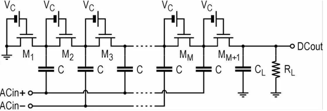
Finally, an auxiliary rectification chain is exploited in [37] (Fig. 2.7) to generate the bias offset voltages needed to compensate the threshold voltage of the transistors of the rectifying chain. Although this arrangement can effectively reduce the dead zone of a RF harvester, it should be considered that the auxiliary chain and associated coupling capacitors involve substantial increase of the circuit physical size and potentially augment power dissipation lowering the whole system efficiency.
Fig. 2.7. Multi-stage rectifier with auxiliary chain for the threshold voltage compensation [37].
2.1.2
Threshold self-compensated rectifier
As shown in the previous section, state-of-art rectifiers for RF energy harvesting systems are unsuitable for batteryless platforms since they rely on either a pre-programming phase or secondary batteries to enhance the system performance. In contrast, the adopted solution allows the desired compensation to be achieved in a fully passive way.
The basic idea is to perform the desired threshold compensation by profitably exploiting the inherent properties of the voltage waveforms at the nodes of the rectifying chain. Indeed, it should be noted that such voltages have:
• equal AC amplitudes (as long as coupling capacitors C are shorted at RF),
• progressively increasing DC components from the input to the output of the rectifying chain.
The latter properties suggests that the bias offset required by each gate terminal can be found in the following nodes of the multiplication chain, rather than calling on auxiliary compensation circuitry. The simplest embodiment of such self-compensation concept was first disclosed in [38]. In this patent, a simple yet effective threshold compensation is achieved by merely connecting the gate of each transistor of the pumping chain to the source of the right-adjacent one instead of shorting it to the drain of the same device, as shown in Fig. 2.8.
Fig. 2.8. Basic implementation of the threshold self-compensation concept [38].
However, this basic implementation may not guarantee substantial performance improvement. Indeed, it provides a bias offset VC equal to the DC
voltage increment due to each doubler stage (i.e. two adjacent rectifying devices), that is roughly VO/N, where VO is the rectifier output voltage and N is the number
and/or low nominal output voltage, the described solution may prove ineffective because of a quite modest compensation voltage (VC).
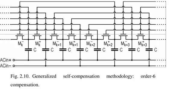
Nevertheless, this approach can be easily generalized thus overcoming its inherent limitations. To this aim, we adopted a self-compensation methodology [39][40], which consists in further extending the length of the compensating bridges to the purpose of increasing the obtained gate bias offset. The “order” of such compensation (i.e. the length of gate connections) is to be chosen depending on the process threshold voltage and the required output voltage. According to this generalized approach the implementation reported in Fig. 2.8 can be considered as an order-2 compensation topology.
It is worth noting that, only even-order compensations are allowed because of the alternating node phases. Indeed, achieving the desired compensation requires the gate terminal of each transistor is connected to a following node of the pumping chain, whose voltage waveform is in phase with that one at the drain of the same device. Order-4 and order-6 solutions are shown in Fig. 2.9 and Fig. 2.10, respectively.
Fig. 2.9. Generalized self-compensation methodology: order-4 compensation.
Fig. 2.10. Generalized self-compensation methodology: order-6 compensation.
The bias offset VC provided by a an order –n compensation topology can be
roughly estimated by assuming that in steady-state conditions the average output voltage of the chain is evenly shared among the rectifying devices. Under such assumption, VC can be easily calculated as:
N nV V 2 O C = (2.4)
As shown in (2.4) the proposed methodology allows the bias offset to be increased by merely extending the length of the compensating bridges.
2.1.3
System design considerations
A block diagram of the RF harvesting system is illustrated in Fig. 2.11 along with the reference notation adopted to the purpose of the circuit analysis. As already explained, the system consists of a receiving antenna to draw the RF power radiated by the hub, an impedance matching network to optimize the power
transfer between the antenna and the rectifying chain, and a voltage rectifier to convert the RF power into DC voltage and current to the load.
Fig. 2.11. Block diagram of the RF energy harvesting system.
The power conversion efficiency (PCE) of the harvesting system is herein defined as the ratio of the load DC power (PL) to the available RF power from the
antenna (PS,AV): AV S, L P P Σ= (2.5)
The main design goal is maximizing the PCE. If the antenna available power is a design constrain, optimizing the PCE results in maximizing the power delivered to a given load. More frequently, the output current and voltage levels are specified in order to comply with the load minimum requirements. Accordingly, PCE optimizations leads to a minimization of the available power at
the antenna connector resulting in the maximization of the node distance from the hub. The latter design case was chosen, as it is more pertinent to our application scenario. Useful considerations about the system can be drawn by expressing the harvester PCE as:
η T G
Σ= A (2.6)
where GA is the available power gain of the matching network (always
lower than 0 dB because of resistive losses), T is the power transmission coefficient at the interface between the matching network and the rectifier, and η is the rectifier inherent efficiency, which is defined as:
M L P
P
η= (2.7)
Moreover, parameters GA and T can be expressed by well-known formulas
[41] as a function of the scattering parameters of the matching network Sij:
2 OUT M, 2 21 2 S 11 2 S AV S, AV M, A 1 1 1 1 Γ S Γ S Γ P P G − − − = = (2.8) 2 IN R, OUT M, 2 IN R, 2 OUT M, AV M, M 1 1 1 Γ Γ Γ Γ P P T − − − = = (2.9)
As apparent from (2.8) and (2.9), GA is a function of the matching network
parameters. Conversely, coefficient T is a function of both the matching network and rectifier parameters. Therefore, according to (2.6), the design of the whole harvesting system cannot be split into two independent optimizations concerning the matching network and the rectifier, respectively. System co-design is needed for an optimum trade-off to be achieved between the rectifier efficiency and its input reflection.
In order to simplify the design task an iterative procedure was developed, which consists in alternatively and repeatedly optimizing the two circuit blocks, namely the rectifier and the matching network. To this aim proper figures of merit were chosen, namely parameters:
T G ΣM = A (2.10) η T ΣR = (2.11)
Which were considered as figures of merit for the optimization of the matching network and the rectifier, respectively. The proposed design algorithm starts with the optimization of the rectifier (with the goal of maximizing ΣR) for a
given output voltage and current levels, assuming a source termination equal to a first-trial value of ΓM,OUT. Evaluated ΓR,IN, the optimization of the matching
network can be performed (with the goal of maximizing ΣM) by assuming a load
termination equal to the estimated ΓR,IN. Then, a new value of ΓM,OUT is obtained.
If this new value is close enough to the initial one, the design procedure is ended, otherwise a new optimization cycle starts with the design of the rectifier assuming a source termination equal to new value of ΓM,OUT, and so on. It is worth noting
that the power reflection coefficient T is embedded both in ΣM and ΣR. Thanks to
this the described iterative procedure is able to converges to the optimization of the whole system PCE splitting the initial design task into two simpler optimizations (see Appendix A), each entailing a lower number of design variables.
2.1.4
Design of the matching network
Impendence matching between the antenna and rectifier is a crucial issue for the optimization of the overall system performance and several studies have been proposed about this topic [42]-[45]. Nevertheless, power losses associated with the matching network have never been formally included in the design flow of a RF energy harvesting system. As long as high-Q components are exploited for impendence matching (e.g. off-chip components), power losses can be neglected. On the other hand, when low-Q matching components are only available and/or high impedance transformation ratio is required (as in [27]), power losses cannot be neglected and care-full co-design is needed to balance losses and reflection. The developed design strategy is the first one that includes power losses of the matching network in the design flow of a energy harvesting system. Indeed, according to (2.8), GA is embedded into metric ΣM which is to be optimized. It is
worth nothing that the proposed methodology is broadly valid, regardless of the matching network topology, transformation ratio, or fabrication means. If power losses are negligible, GA ≈ 1 and ΣM ≈ T. Hence, optimizing ΣM leads to perfect
eventually entail a residual impedance mismatch at the rectifier’s input for the sake of losses minimization. The proposed design is a typical example of this latter case. Indeed, a general purpose 50-Ω antenna was assumed as source, which entails a large impedance transformation ratio. Moreover, on-chip components were exploited for impedance matching, hence suffering from limited Q values. Fig. 2.12 shows the schematic of the adopted matching network, which was chosen on the basis of a preliminary comparative study between different matching network topologies.
Fig. 2.12. Schematic of the adopted matching network.
According to the aforementioned design methodology, matching network is to be designed with the aim of maximizing ΣM for a given load termination. In
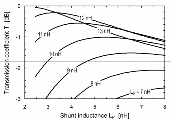
Fig. 2.13 is shown ΣM as a function of LS and LP at 915 MHz. On-chip and
package parasitics were taken into account (namely 300-fF bond-pad capacitance and 2-nH wire bonding inductance with a Q of 20 at 900 MHz). For the sake of simplicity the curves reported in Fig. 2.13 were obtained assuming a load
impedance equal to 760 Ω // 1.5 pF (ΓR,IN = 0.613 – j 0.652), which is the actual
input impedance of the rectifier at the end of the design iteration.
Fig. 2.13. Simulated ΣM versus LP for different values of LS (f = 915 MHz, ΓR,IN = 0.613 – j 0.652).
According to the results reported in Fig. 2.13, a series inductance of 11 nH and a shunt inductance of 6.8 nH is needed for optimum design. This choice results in a maximum ΣM of –2.45 dB with GA = –1.56 dB and T = –0.89 dB
(Fig. 2.14). Note that, the designed matching network is far from guarantee the maximum power transfer (i.e. T = 0 dB). Nevertheless, this design provides the best trade-off between losses and reflection. Basically, different values of LS and
LP are needed to optimize T. However, the best-T solution would lead to a poorer
Fig. 2.14. Simulated transmission coefficient T as a function of LP for different values of LS (f = 915 MHz, ΓR,IN = 0.613 – j 0.652).
2.1.5
Design of the rectifier
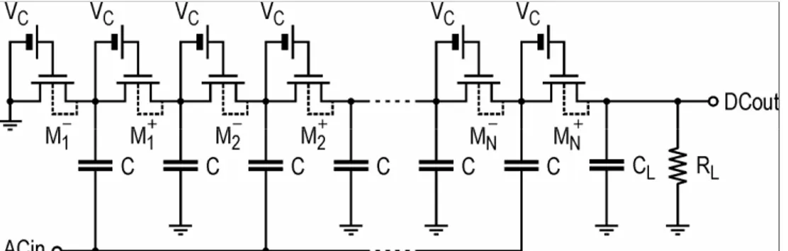
NMOS transistors with isolated bodies were used for this design, thanks to the availability of a deep n-well layer in the adopted fabrication process. Moreover a static connection of the body to the source terminal of each pumping device was adopted, rather than exploiting a dynamic control of the well voltage as proposed in [46], since this strategy proves ineffective under very low pumping voltage conditions, as typical for micro-power RF energy harvester.
Three key parameters are to be determined for the deign of the threshold self-compensated rectifier, namely the number of cascaded stages N, the gate width of pumping devices W, and the compensation voltage VC. The transistor
process) in order to optimize the RF performance, whereas the coupling capacitors
C are large enough to avoid affecting the conversion efficiency. The design goal is maximizing ΣR for a given source termination. As already mentioned, the output
DC voltage and current levels should be considered as design constraints, according to the load minimum requirements. On the basis of a preliminary feasibility study, a 1.2-V output voltage on a 1-MΩ load (i.e. 1.2-µA output current) was assumed as the nominal design target. Thus an output-constrained parametric analysis of ΣR was carried out according to such assumption. To ease
this analysis, circuit simulations were initially performed by recourse to the simplified schematic shown in Fig. 2.15, where the threshold compensation voltage is applied through ideal DC voltage sources VC.
Fig. 2.15. Simplified schematic of a threshold-compensated multi-stage rectifier.
Once determined the optimum value for VC, ideal voltage sources can be
replaced by the proposed forward gate connections, compensation order being chosen in order to best fit the designed gate bias offset under nominal operating
conditions. Note that the simulated performance of the simplified topology (Fig. 2.15) is really close to the one of the real circuit with gate bridges.
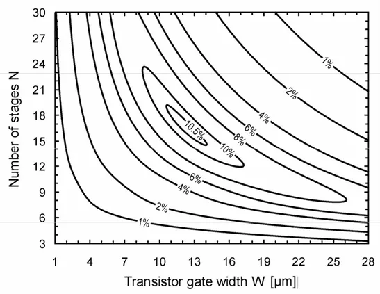
Fig. 2.16 displays the typical dependence of ΣR on N and W for a given
value of VC. The contour plots of η and T are also reported in Fig. 2.17. For the
sake of simplicity these plots were calculated assuming a source impedance of 300 Ω // 20.2 nH (ΓM,OUT = 0.508 + j 0.557) which is the actual output impedance
of the matching network at the end of the design flow.
Fig. 2.16. Simulated percentage ΣR versus N and W for a compensation voltage VC of 240 mV (VO = 1.2 V, RL = 1 MΩ, L = 90 nm, CL = 47 nF,
C = 3 pF, f = 915 MHz, ΓM,OUT = 0.508 + j 0.557).
As apparent from Fig. 2.16, optimum values of both N and W can be identified for a given value of VC.
This behaviour is well-known and consistent with previously reported analysis [33][42][43] As a matter of fact, the rectifiers’ inherent efficiency decreases with the number of stages N, but a too low stage count would result in a excessively high input impedance, i.e. high power reflection. Similarly, increasing the transistors’ gate with W favours direct conduction, thus increasing efficiency. However, too large devices would eventually entail excessive parasitic losses and reverse (leakage) conduction.
Fig. 2.17. Simulated contour plots of η (a) and T (b) as a function of N and W for a compensation voltage VC of 240 mV (VO = 1.2 V,
RL = 1 MΩ, L = 90 nm, CL = 47 nF, C = 3 pF, f = 915 MHz, ΓM,OUT = 0.508 + j 0.557).
Interestingly, the peculiar dependence of ΣR on N and W displayed in
Fig. 2.16 keeps qualitatively unchanged as compensation voltage VC is varied.
Fig. 2.18. Optimized ΣR versus VC (VO = 1.2 V, RL = 1 MΩ, L = 90 nm,
CL = 47 nF, C = 3 pF, f = 915 MHz, ΓM,OUT = 0.508 + j 0.557).
This plot reveals that an optimum value exits for VC as well, which results in
a global maximization of ΣR. Note that, such optimum VC value is quite far from
the typical threshold voltage of the adopted technology, which is around 0.45 V. Indeed, increasing VC improves the transistors’ conductivity, but worsens their
rectifier behaviour (i.e. the reverse conduction increase) [40]. Therefore a fair trade-off is needed to achieve the best performance.
According to the performed parametric analysis (Fig. 2.16 and Fig. 2.18), a 17-stage rectifier topology was adopted for optimum design along with a 12-µm transistor width and a compensation voltage of 240 mV. The latter was implemented exploiting an order-6 compensation topology (Fig. 2.10).
Concerning this, It should be observed that the gates of the last 5 transistors of a order-6 self-compensated NMOS rectifier require DC voltages higher than the delivered one. In general this problem affects the last n-1 transistors of an order-n compensated topology. This issue was addressed by cascading an additional “dummy” chain to generate higher DC voltage to be used for the threshold compensation of the last transistors of the pumping chain.
The tail end of the designed rectifier is shown in Fig. 2.19. The last transistor of the pumping chain (M17+) is purposely uncompensated to limit the reverse leakage current of the rectifier. For the designed rectifier, a ΣR of 10.6%
was simulated at VO = 1.2 V on a 1-MΩ load.
Fig. 2.19. Schematic of the rectifier’s tail end with additional dummy chain.
2.1.6
Harvester simulated performance
The designed energy harvesting system consists of an improved 17-stages rectifier (Fig. 2.10),exploiting a fully passive threshold self-compensation scheme, and an integrated matching network (Fig. 2.12) which allows interfacing the rectifier with a general purpose 50-Ω antenna. The system operates in the 915-MHz ISM band. Following the developed design methodology a simulated ΣR
of 10.6% was achieved (assuming an output voltage of 1.2-V on a 1-MΩ load) with a GA of -1.56 dB. Thus, according to (2.6) a PCE of 7.4% was estimated for
the overall harvesting system. Therefore, it is able to provide a 1.2-µA output current on a 1-MΩ load with an available input power at the antenna of -17.1dBm.
2.2
Power management unit
The energy collected by the RF harvester is accumulated in a storage capacitor and properly used to supply the whole system. Implementing an active transmission scheme entails a transceiver energy budget that can only be accomplished by adopting a convenient power management strategy, which is based on a duty-cycled operation mode (“charge & burst”) of the RF front-end (Fig. 2.20). As the hub illuminates the network by radiating its FSK-modulated carrier, the harvesting unit of each sensor node starts charging the storage capacitor (charge phase). The power management unit monitors the charge status of the storage capacitor by sensing its voltage drop and turns the RF front-end on as soon as a fair supply level is reached (VSTORE(high) in Fig. 2.20). After being
interrogation by the hub. If an interrogation is detected within the code sent by the hub, a transmit phase follows, in order to answer to the hub.
Fig. 2.20. Power management strategy (charge & burst).
The current consumption associated to the listen and transmit phases progressively discharges the storage capacitor, since the instantaneous supply power required by the RF front-end is much higher than the harvested one. Therefore, as the voltage drop across the storage capacitor reaches a predefined minimum value (V in Fig 2.20), the power management unit turns the RF
front-end off and a new charge phase starts. The main benefit resulting from the charge & burst procedure lies in the possibility to spend in a relatively short time interval (listen and transmit phases) the energy accumulated in a quite longer phase (charge phase). Indicating with δ the duty cycle of the transceiver on/off commutation, the adopted strategy results in an available supply power which is 1/δ times higher than the harvested one. For instance, if a 1-µW power is continuously harvested from the incoming RF signal and the system is operated with a 1‰ duty cycle, then a 1-mW power is available to supply the transceiver during the operating phase. This key feature enables active transmission at 2.45-GHz. A block diagram of the power management unit is shown in Fig. 2.21.
Fig. 2.21. Block diagram of the power management unit.
It manly consists of a voltage reference, an hysteresis comparator, a voltage regulator and a voltage limiter. During the charge phase, the hysteresis comparator senses the voltage drop across the storage capacitor and turns the
voltage regulator on as soon as a 1.6-V supply voltage (VSTORE(high)) is reached.
After being turned on, the voltage regulator is able to deliver 1-V supply voltage to the RF front-end, with a maximum output current of 1 mA. During this phase, the storage capacitor discharges rapidly till a predefined low voltage (VSTORE(low)),
set to 1.2 V. Then, the comparator turns the regulator off allowing the harvester to recharge the storage capacitor.
Nano-power circuits were extensively adopted for the power management unit design in order to guarantee negligible power consumption (lower than 100 nA) during the charge phase improving the harvester efficiency and charge rate.
Moreover, the power management unit includes a voltage limiter, which was designed to clamp the unregulated voltage (VSTORE) if the maximum safe level
is overcome. Concerning this, ultra-thick-gate-oxide transistors were extensively used for the design of the power management unit circuits to guarantee safe operation with an unregulated voltage up to 1.8 V.
2.2.1
Voltage reference
The voltage reference is the most critical block of the power management unit. Indeed, an accurate voltage reference is needed for proper operation of the whole system. This reference should be able to operate with a low supply voltage, be independent of VSTORE variations, exhibit a good temperature stability and have
an extremely low current consumption.
used. REF1 was designed for nA-level current consumption, whereas REF2 exhibits a better stability over temperature and supply voltage variations at the cost of a higher current consumption. The two references are alternatively enabled during each system operating cycle, specifically, REF1 during the charge phase and REF2 during the discharge phase (i.e. listen and transmit phases). This allows achieving both minimal off-state (charge phase) current leakage and high on-state (discharge phase) accuracy.
The schematics of REF1 and REF2 are shown in Fig. 2.22 and Fig. 2.23, respectively. REF1 was implemented exploiting a self-biased current reference based on ∆VBE and a MOS transistor (M5) working below saturation (PTAT2
configuration) [47][48], which allows an extremely low current consumption to be achieved with a substantial silicon area savings.
The ∆VBE-based current mirror was designed using parasitic npn bipolar
transistors (Q1 and Q2). Assuming that the current mirror M1-M2 has a ratio 1:1,
the IPTAT2 current can be expressed as:
( )
[
]
2 2 4 4 4 2 3 3 3 2 C V L W K L W K IPTAT2 T ln ≅ (2.12) Where 2 1 E E A A C = , and K =µ
nCox.To cancel the quadratic dependence from the temperature, the current IPTAT2
is fed via transistor M3 to the diode-connected transistor M4, which was sized in
simulated temperature coefficient of 160 ppm /°C at 1.6 V with an extremely low current consumption (≈ 40 nA).
Fig. 2.22. Schematic of the nano-amp voltage reference (REF1).
REF2 operates during the listen and transmit phases. During this phases the unregulated supply voltage (VSTORE) experiences a fast and large variation, from
1.6 V to 1.2 V. Therefore, unlike REF1 which has to be accurate just at 1.6 V,
REF2 must be able to guarantee accuracy in a wide range of supply voltage. To this purpose, a self-biased PTAT current reference with resistor (R) was used to implement REF2, as shown in Fig. 2.23.
This solution allows achieving a better accuracy and stability over supply voltage variations at the cost of a much higher current consumption. However,
most power-hungry component of the designed transceiver. The PTAT current is fed to a diode-connected transistor (M4) working in sub-threshold in order to
guarantee the temperature compensation with the suppression of the temperature dependence of the charge carrier mobility [47].
Fig. 2.23. Schematic of the PTAT-based voltage reference (REF2).
REF2 was designed to provide a voltage of 0.6 V and exhibits a simulated temperature coefficient of 53 ppm/°C. The simulated temperature dependence of
Fig. 2.24. Simulated temperature dependence of the voltage reference
REF1 (VSTORE = 1.6 V).
2.2.2
Hysteresis comparator
The hysteresis comparator provides a logic level “1” at its output (enable
signal) when the unregulated supply voltage (VSTORE) reaches the predefined high
level VSTORE(high). Conversely, the enable signal is set to the logic level “0” when
VSTORE drops below the predefined low level VSTORE(low), as shown in Fig. 2.26.
Fig. 2.26. Hysteretic characteristic of the comparator.
Fig. 2.27 displays the schematic of the designed hysteresis comparator. It is based on a two-stage amplifier with a differential input pair (M1-M2) and a
diode-connected transistor string used to detect the unregulated voltage. Switches
Msw1 and Msw2 (properly controlled by the enable signal) allow implementing the
“hysteretic characteristic” with threshold voltages VSTORE(high) and VSTORE(low).
Concerning this, it is worth noting that, as the enable signal goes high, the transistor count of the sensing string is reduced thanks to the switch Msw3.
![Fig. 2.4. Multi-stage rectifier with threshold compensation through voltage generator and distributor [31]](https://thumb-eu.123doks.com/thumbv2/123dokorg/4475589.32135/33.892.195.745.441.805/multi-stage-rectifier-threshold-compensation-voltage-generator-distributor.webp)
![Fig. 2.5. Rectifier with passive mirror-like threshold compensator [32].](https://thumb-eu.123doks.com/thumbv2/123dokorg/4475589.32135/34.892.192.748.360.566/fig-rectifier-passive-mirror-like-threshold-compensator.webp)
![Fig. 2.7. Multi-stage rectifier with auxiliary chain for the threshold voltage compensation [37]](https://thumb-eu.123doks.com/thumbv2/123dokorg/4475589.32135/36.892.195.745.146.488/multi-stage-rectifier-auxiliary-chain-threshold-voltage-compensation.webp)