2
SURFACE PREPARATION AND
CHARACTERIZATION OF
SEMIPOLAR (20-21) INGAN LAYERS
Relatore: Presentata da:
Prof.ssa Daniela Cavalcoli Julian Plaickner
Correlatore: Prof. Patrick Vogt
Sessione III
i
Index
Abstract
iii
Introduction
1
Chapter 1 – Overview on nitride semiconductors
1.1 Crystal structure . . . 31.2 Polarity . . . 4
1.3 Polarization fields . . . 6
1.4 Energy gap . . . 8
1.5 Surface electron accumulation . . . 9
1.6 Heteroepitaxial growth . . . 11
Chapter 2 – The semipolar (20-21) surface
2.1 Surface reconstructions . . . 152.2 Morphology of (20-21)-GaN samples . . . 17
2.3 Semipolar GaN substrates . . . 19
2.4 Indium incorporation and critical thickness . . . 21
2.5 Semipolar InGaN LEDs . . . 23
Chapter 3 – Surface-analytic experimental techniques
3.1 Surface physics . . . 273.1.1 General considerations . . . 28
3.1.2 Ultra high vacuum (UHV) . . . 28
3.1.3 Surface preparation . . . 30
3.2 Electron spectroscopy . . . 30
3.2.1 X-ray Photoelectron Spectroscopy (XPS) . . . 31
3.2.2 Interpretation of XPS spectra . . . 33
3.2.3 Auger Electron Spectroscopy (AES). . . 35
3.3 Scanning probe microscopy (SPM) . . . 37
3.3.1 Working principle of SPM . . . 37
3.3.2 Atomic force microscopy (AFM) . . . 38
3.3.3 Scanning tunneling microscopy (STM) . . . 40
3.4 Surface Photovoltage Spectroscopy (SPS) . . . 42
ii
Chapter 4 – Surface preparation and structural properties
4.1 Properties of studied InGaN samples . . . 47
4.2 Morphology of oxidized surface . . . 48
4.3 Thermal annealing . . . 50
4.4 Stoichiometry . . . 52
4.5 Polarity determination by XPS . . . 53
4.6 Surface reconstructions by LEED . . . 55
Chapter 5 – Electronic and optical properties
5.1 Calibration of STM on HOPG films . . . 575.2 STM images of the InGaN samples . . . 59
5.3 Band bending . . . 61
5.4 SPS measurements . . . 64
5.5 STS measurements . . . 70
5.6 Optical transmission studies . . . 72
Summary and conclusions
75
References
77
iii
Abstract
In questa tesi vengono studiate le proprietà fisiche della superficie di eterostrutture InGaN/GaN cresciute con orientazione semipolare (20-21). Questi materiali fornirebbero una valida alternativa alle eterostrutture cresciute secondo la tradizionale direzione di crescita polare (0001) per la realizzazione di LED e diodi laser. I dispositivi cresciuti con orientazione semipolare (20-21) sono studiati soltanto da pochi anni e hanno già fornito dei risultati che incitano significativamente il proseguimento della ricerca in questo campo. Oltre all’ottimizzazione dell’efficienza di questi dispositivi, sono richieste ulteriori ricerche al fine di raccogliere delle informazioni mancanti come un chiaro modello strutturale della superficie (20-21). I capitoli 1 e 2 forniscono un quadro generale sul vasto campo dei semiconduttori basati sui nitruri del terzo gruppo. Il capitolo 1 tratta le proprietà generali, come le caratteristiche della struttura cristallina della wurtzite, l’energy gap e il più comune metodo di crescita epitassiale. Il capitolo 2 tratta le proprietà specifiche della superficie (20-21) come struttura, morfologia e proprietà legate all’eterostruttura InGaN/GaN (incorporazione di indio, strain e spessore critico).
Nel capitolo 3 vengono descritte sinteticamente le tecniche sperimentali utilizzate per studiare i campioni di InGaN. Molte di queste tecniche richiedono condizioni operative di alto vuoto e appositi metodi di preparazione superficiale.
Nel capitolo 4 vengono discussi i risultati sperimentali riguardanti la preparazione superficiale e le proprietà strutturali dei campioni. Il trattamento termico in ambiente ricco di azoto si rivela essere un metodo molto efficiente per ottenere superfici pulite. La superficie dei campioni presenta una morfologia ondulatoria e una cella unitaria superficiale di forma rettangolare.
Nel capitolo 4 vengono discussi i risultati sperimentali relativi alle proprietà elettroniche e ottiche dei campioni. Immagini alla risoluzione atomica rivelano la presenza di ondulazioni alla scala dei nanometri. Vengono misurati l’energy gap e l’incurvamento superficiale della bande. Inoltre vengono identificate una serie di transizioni interbanda dovute all’interfaccia InGaN/GaN.
iv In this thesis, the physical properties of the surface of semipolar (20-21) InGaN/GaN heterostructures are investigated. These materials should provide an adequate alternative to (0001)-oriented heterostructures for the realization of high efficiency light emitting diodes (LEDs) and laser diodes (LDs). Semipolar (20-21)-oriented devices are studied only by a few years and have already showed good results, providing an incentive to continue the research in this field. In addition to the optimization of the efficiency of the devices, further investigations are required in order to understand remaining issues such as the development of a structural model of the (20-21) surface.
Chapters 1 and 2 give an overview on the extensive field of the III-nitride semiconductors. Chapter 1 deals with the general properties, i.e. structural properties related to the wurtzite crystal structure, the energy gap and the most common heteroepitaxial growth method. Chapter 2 deals with specific properties of the semipolar (20-21) surface (structure and morphology) and of the InGaN/GaN heterostructures (indium incorporation, stress relaxation and critical thickness).
Chapter 3 gives an overview on the experimental surface-analytic techniques used to investigate the InGaN samples. Most of these techniques require ultra-high vacuum conditions and appropriate surface preparation methods.
In chapter 4, we present the experimental results concerning the surface preparation and structural properties of the studied samples. Thermal annealing in nitrogen ambient is found to be a very efficient method to obtain clean InGaN surfaces. The surface of the samples exhibit a undulated morphology and a cubic-like surface unit cell.
In chapter 5 we consider the results concerning the electronic and optical properties. Atomic-resolved images of the surface reveal the presence of undulations at the nanoscale. The energy gap and the surface band bending are measured. Further, a set of interband transitions related to the InGaN/GaN interface are identified.
1
Introduction
The III-V semiconductors (like AsGa, InP) were systematically investigated since the 1950s: they are also called classical semiconductors. In contrast, the research on III-nitride semiconductors (like GaN, InN) started many years later. This is also due to the fact that growth and physical properties of these materials present many challenges. On the other hand, the so-called III-nitrides in the form of ternary compounds (AlGaN, InGaN, AlInN) offer the opportunity to tune the band gap and hence the emission wavelength of opto-electronic devices such as light emitting diodes (LEDs), laser diodes and photo-detectors over a wide spectral range from the ultra violet over the whole visible region.
Since the demonstration of the first III-nitride light-emitting devices (LEDs) and laser diodes (LDs) in the early 1990s, significant advances has been realized towards increasing device efficiency, improving device reliability and developing advanced device designs for high-power applications [1]. Although progress has been considerable, current commercially available III-nitride LEDs and LDs are still grown on the (0001) c-plane of the wurtzite crystal structure and their performance is nonetheless affected by the presence of polarization-related electric fields. When III-nitride heterostructures are grown along the c-axis, fixed polarization-related sheet charges at interfaces can result in large internal electric fields. These fields can create several issues for III-nitride LEDs and LDs, including reductions in the radiative combination rate due to spatial separation of the electron and hole wavefunctions, i.e. phenomenon referred to as Quantum Confined Stark Effect (QCSE), and blueshifts in the peak emission wavelength with increasing carrier density.
In 2000, Waltereit et al clearly demonstrated the absence of internal electric fields in m-plane GaN quantum wells, triggering a worldwide research effort in nonpolar and semipolar III-nitride semiconductors [1]. In addition to the significant reduction of the polarization fields, the growth of nitride heterostructures along non- and semipolar orientations yields a number of new design options to control the optoelectronic properties of the light emitters. Today, the understanding of polar, semipolar and nonpolar nitrides has made leaps forward. However, there is a wide range of topics related to the III-nitrides like growth and heteroepitaxy, theory and modeling, optical and electronic properties, and there remains still challenges and open issues [2].
These studies are of major importance for the role played by InGaN in many optoelectronic applications. Group-III nitride based laser diodes
2 and light emitting devices in the visible spectrum employ InGaN quantum wells as active regions. Several crystal orientations for the growth of InGaN quantum wells are of interest for such devices. The technological setup for the realization of InGaN based heterostructures and devices has been developed only recently and the efficiency of these devices depends on several factors like growth quality, crystal orientation and surface preparation. Therefore, there still remain a variety of experimental investigations to perform in order to obtain an adequate overview on efficiency and properties of such devices.
3
Chapter 1
Overview on nitride semiconductors
In this chapter, a brief overview on III-nitride semiconductors is given. Beside of structure-dependent properties related to the wurtzite crystal structure such as polarity and polarization fields, widely treated in literature, also the recently studied phenomenon of surface electron accumulation is considered. The most common heteroepitaxial growth method of III-nitrides is described. The properties of III-III-nitrides which are related in a specific way to the semipolar (20-21) crystal orientation are reported in chapter 2.
1.1 Crystal structure
III-nitride semiconductor compounds crystallize in either the hexagonal wurtzite structure or in the cubic zincblende structure (figure 1.1), which are closely related to each other. In both cases, each group-III atom is tetrahedrally coordinated by four nitrogen atoms. The main difference between the two crystal structures is the stacking sequence of the close packed diatomic planes. The stacking sequences are ABABAB along the wurtzite [0001] directions and ACBACB along the zincblende [111] directions. This difference results in distinct space group symmetries,
FIG. 1.1. Unit cell of III-nitrides with a) zincblende and b) wurtzite crystal structure (top view and side view) [3].
P63mc for wurtzite and F43m for zincblende [4]. Wurtzite structure
consists of two embedded hexagonal atom stacks along the
4 direction and is also called hexagonal closest packings (hcp). To indicate direction, axis and planes of the wurtzite crystal structure, a modified Miller-Bravais notation {hkil} is employed, where i = -(h+k). When h = k = i = 0 and l = 1, then this (0001) plane is called c-plane and the perpendicular direction to this plane is called c-direction or [0001] [5].
The c-plane of wurtzite III-nitrides is also called polar plane, whereas the other crystal planes are called semi-polar or non-polar planes (figure 1.2). In contrast to the polar structure of III-nitrides, the semi-polar
FIG. 1.2. Different crystallographic orientations in the wurtzite unit cell [6].
and non-polar structures exhibit two-fold surface symmetry instead of the six-fold symmetry: this has an impact on many physical properties of the material. For example, the microstructure of nonpolar and semipolar heteroepitaxial films is drastically different from that of films deposited along the polar direction. A different microstructure gives rise to different type of defects from which electrical and optical properties depend.
1.2 Polarity
An important structural property is the polarity, a term that refers to the atoms lying at the topmost of the bare layer surface, i.e. the surface with the least number of broken bonds. For III-nitrides the surface can be N-polar or group-III-N-polar. It’s important to distinguish between N-polarity and surface termination. As clarified by the example showed in figure 1.3, the same atom can lie at the topmost of the surface for two different polarities. The polarity of III-nitrides depends on the growth conditions. Polarity control of III-nitrides is an important issue, on which thermal and optical properties, as well as chemical and internal stability strongly depend.
semipolar nonpolar
5
FIG. 1.3. Ball and stick model illustrating the In-polarity [0001] and the N-polarity [000-1] directions of the wurtziteInN. The surfaces are both shown with In termination [7].
The commonly used methods for InN and GaN polarity determination are convergent beam electron diffraction (CBED) [8] and wet etching [9]. Nevertheless, these methods have some limitations. The thickness and crystal quality of the investigated layers must be sufficiently high to achieve clear diffraction spots, required for polarity determination by CBED. In the case of wet etching, different crystal facets may etch slower or faster leading to difficulties in polarity determination. As reported recently by D. Skuridina et al. [10], X-ray Electron Spectroscopy (XPS) is a suitable technique for polarity determination of InN and GaN layers with different surface orientations (0001), (000-1) and (11-22). The method is based on the observation of a peak preference in the valence band (VB) spectrum:
The peak at lower binding energy is mainly associated with p-like orbital states and dominates for group-III polar samples.
The peak at higher binding energy has a partial contribution of s-like states and dominates for N-polar samples.
In comparison to other polarity determination methods, Polarity determination by XPS is non-destructive and also suitable for oxidized layers with rough surface.
The fact that photoelectrons emitted from the surface are affected by the polarization field in the crystal might explain the origin of the differences in VB states at low and high binding energies. The presence of a
6 polarization field is related to the wurtzite crystal symmetry (as explained in section 1.3) and also to the large electronegativity difference between nitrogen and group-III atoms. However, similar peak dependences of the VB states with respect to the crystal polarity were observed also for wurtzite II-VI semiconductors, such as ZnO and CdS [11]. The origin of the correlation between VB peak and crystal polarity is not yet fully understood.
1.3 Polarization fields
The presence of polarization is strongly connected to the unit cell symmetry of the crystal. In the absence of external electric fields, the total macroscopic polarization of a solid is the sum of the spontaneous polarization of the equilibrium structure and of the strain-induced piezoelectric polarization.
The zincblende compound semiconductors have four symmetry equivalent polar axes whose contributions cancel each other in equilibrium. Hence, these materials don’t exhibit a spontaneous polarization. In contrast, the wurtzite structure has a singular polar axis, the c-axis, along which the structure exhibit a spontaneous polarization. Semiconductor layers are often grown under strain due to the lattice mismatch to the underlying layer. The strain produces a deformation of the unit cell which can lead to an additional polarization. In the case of the zincblende, the growth along one of the polar axes lift the symmetry and the crystal exhibit therefore a piezoelectric polarization. The wurtzite structure with its unique polar axis always carries piezoelectric polarization for any growth direction [4].
FIG. 1.4. Microscopic picture of spontaneous polarization in a free-standing GaN slab [4].
7
A way to illustrate the spontaneous polarization is showed in figure 1.4. Each unit cell can be thought to contain a charge dipole that is formed due to the spatial separation of the barycenter of the negative charges (electron clouds) and the positive charges (atomic nuclei). The dipoles in every layer of unit cells neutralize each other in the bulk of the semiconductor, but form sheet charges on the surfaces. A free Ga-face surface develops a negative sheet charge and a positive sheet charge forms on the N-face. The surface polarization charge density for GaN is of the order of 1013 cm-2.
These charges are large enough to affect the electrical properties of a material drastically at surfaces and interfaces. Since the atomic sheet density in nitride semiconductors is 1015 cm-2, roughly 1% of the atoms contribute
to the polarization charge.
The phenomenon of polarization is important for applications in microelectronics. For example, the spontaneous polarization generate a two-dimensional electron gas (2DEG) in a AlInN/GaN heterostructure sand this gives rise to high performance high electron mobility transistors (HEMTs) [12]. The knowledge of the polarization component ΔPz along
the growth direction is also important for the understanding of the behavior of optoelectronic devices. This component was calculated under the assumption of full strained epitaxial layers by Romanov et al. [13].
FIG. 1.5. Polarization component along growth direction as function of the angle between growth direction and c-direction for a) AlGaN and b) InGaN on a GaN substrate [6].
ΔPz is shown as function of the angle between growth direction and
c-direction in figure 1.5. ΔPz is maximal for growth along the c-direction and
is reduced for every different growth orientation. It vanishes at two different angles, which are influenced in a very small extent by the alloy composition.
8
1.5 Energy gap
Early optical absorption studies on sputtered InN films suggested a fundamental gap of 1.9 eV. However, further measurements on InN films grown by Molecular Beam Epitaxy (MBE) indicated a fundamental gap of 0.7 eV. Therefore, it has become necessary to reevaluate many of the material parameters of InN and the composition dependence of the bandgap of all group-III nitride alloys. In fact, the discovery of the narrow bandgap of InN has extended the spectral range of the group III-nitride ternary alloy system, which can now be tuned from the near infrared at 0.7 eV to the deep ultra-violet at 6.2 eV. This wide spectral range offers novel possibilities for the use of group-III nitrides in a variety of device applications. For instance, the energy gaps available in the InGaN alloy system provide an almost perfect match with the full solar spectrum, which makes InGaN a potential material for high efficiency multi-junction solar cells [14].
FIG. 1.7. Energy gap of wurtzite (solid curves) and zincblende (dashed curves) nitride semiconductor alloys and binaries (points) [15].
The energy gaps of wurtzite and zincblende nitride semiconductor alloys are plotted in figure 1.7 as function of lattice constant. A more detailed study of the bandgap is reported in more recent works [16]. The
9
composition dependences of the energy gaps for the ternary alloys AlGaN, InGaN, AlInN satisfy the quadratic form
1
( ) (1 ) ( ) ( ) (1 )
g x x g g
E A B x E A xE B bx x
where the so-called bowing parameter b accounts for the deviation from a linear interpolation between the two binaries A and B. The bowing parameter is always positive for these materials, which reflects a reduction of the alloy energy gaps. Up to now, no agreement has been reached on the bowing parameter value and even on the issue if a single bowing parameter can describe the gaps over its entire composition range [17].
The temperature dependence of the energy gap is usually parameterized using the semi-empirical Varshni formula
2 ( ) ( 0) g g T E T E T T
where α and β are independent parameters that are specific to each system. These parameters are generally sufficient to describe the conduction and valence band structures of bulk nitride materials [15]. However, as the growth conditions and sample structure vary from one sample to another, the reported values for α and β in literature cannot be generalized to characterize a given semiconductor compound. Here one of the major problems arises from the heteroepitaxial relationship between substrate and nitride layers. Since epitaxially grown heterostructures routinely combine layers of lattice-mismatched constituents, the material properties under strain must also be specified. This is conventionally done within the deformation potential theory.
1.6 Surface electron accumulation
In a compound semiconductor, at a certain energy, called the branch-point energy, the valence band (VB) and the conduction band (CB) states change their character from donor-like to acceptor-like. If we have a low Γ-point conduction band minimum (CBM) with respect to the branch-point energy we speak about surface electron accumulation [5]. This phenomenon has attracted much attention since a high surface electron density implies a great technological importance. Surface electron accumulation was observed to be an intrinsic property of InN with different surface orientations [18], [19]. For InGaN and AlInN alloys, a transition from
10 electron accumulation to electron depletion was observed. The mean reason of the appearance of electron accumulation on the surface of InN and related alloys was attributed to In-In metallic bonds, leading to occupied surface states above the CBM.
FIG.1.8. Variation of bandgap and barrier height at (0001)-InGaN surfaces with different indium concentrations in presence of a native oxide. Insets (b) and (c) depict the upward band bending in a depletion layer at a GaN surface and the downward band bending in an accumulation layer at an InN surface, respectively [20].
The composition dependence of the Fermi-level position with respect to the band edges for oxidized (0001) surfaces of n-type InGaN films was investigated using x-ray photoemission spectroscopy (XPS) by Veal et al [20]. The surface Fermi-level position varies from high above the CBM at InN surfaces to significantly below the CBM at GaN surfaces. The surface preparation would require a different method to be optimized for each InGaN composition, consequently, the composition dependence of the Fermi-level pinning has been studied in the presence of the native oxide on the surfaces. The separation between CBM and surface Fermi level, called barrier height ΦB, has been determined from the photoemission data
11
Two possible situations occur:
ΦB > 0: Fermi level pinning in the band gap
ΦB < 0: Fermi level pinning within the conduction band
The composition dependence of the barrier height is estimated by the least squares method to be
2
0.95 2.1 0.53
B x x
From this equation it can be found that the barrier height is zero, i.e. the surface Fermi level coincides with the CBM, at x = 0.29. This composition does not necessarily coincide with the transition from surface electron depletion to accumulation as the nature of the space charge region is determined in a particular sample by whether the bulk Fermi level is above or below the surface Fermi level. However, it is expected that the transition occurs at a value quite close to the zero of the barrier height.
The knowledge of the surface Fermi level is important for surface sensitive devices, such as chemical and biological sensors, where an InGaN active layer is exposed to the environment.
1.7 Heteroepitaxial growth
The growth of high quality epitaxial layers, i.e. layers with a smooth morphology and a low defect density, is the basis for fundamental study and device fabrication. In recent years, the most suitable growth technique for III-nitrides has been found to be Metal Organic Vapor Phase Epitaxy (MOVPE). MOVPE growth is conducted under near thermodynamic equilibrium conditions which rely on vapor transport of precursors in a heated zone. In order to create there near equilibrium conditions, a substrate is typically located on a heated susceptor in the heated zone. The growth occurs via the decomposition of the precursors over the heated substrates. During growth, several processes like adsorption, surface migration and chemical reactions occur. A picture of the processes involved during MOVPE growth is illustrated in figure 1.9.
12
FIG. 1.9. Scheme of the surface processes involved during the MOVPE growth [5].
Basically, there are six reaction steps during the MOVPE growth, which occur simultaneously:
1. Transport of the precursor molecules from the sources to the heated zone.
2. The species resulting from the gas phase decomposition can diffuse on the surface and incorporate into the layer.
3. Terrace diffusion
4. Step-down diffusion (significant only a high temperature) 5. Desorption
6. By-products processes
For the complex MOVPE system the overall reaction rate in the reactor is controlled by:
Thermodynamics: determines the driving force and the direction of the reaction
Kinetics: determines the rates of change in the concentration of reactants in the chemical reaction
13
Hydrodynamics: determines fluid flow, heat transfer and chemical transport of species
Because of the dependence on the thermal decomposition of the precursors, the MOVPE growth process strongly depends on growth temperature and on the amount of the precursors. A qualitative picture of the effect of substrate temperature and reactor pressure on growth rate of the layer is shown in figure 1.10. At very high growth temperature, desorption is dominating.
FIG. 1.10. Qualitative picture of the effect of a) substrate temperature and b) reactor pressure on growth rate of the layer [5].
If the growth temperature is very low, the decomposition of precursors is less and hence the growth rate decreases. The stability of the group-III precursors is very important since it decides which growth temperature is necessary for epitaxy. Morphology and structure of the epitaxial layer depend strongly on the growth conditions, i.e. temperature, precursor and substrate. All of them contribute to different morphologies and structures
a)
14 of the grown layers. The growth process of the layer might be followed different growth modes. The growth of epitaxial layers on a single crystal surface depends significantly on the interaction strength between atoms and the surface.
In the choice of the substrate for the growth of III-nitrides, different aspects should be taken into account:
Thermal expansion and lattice mismatches: they strongly affect growth process and quality of epitaxial layers,
Thermal stability: an easily decomposed substrate at high temperature might be a source for unintentionally contaminations in epitaxial layers
Polarity: the polarity of the substrate leads to growth of different polarity of epitaxial layer.
The control of growth orientation is very important since on which structure, morphology, electrical and optical properties strongly depend. III-nitrides having different polarities shows different thermal stability and different amount of contaminations. Despite the high lattice mismatch respect to III-nitrides, sapphire is still most a widely used substrate due to a low-cost production, thermal stability and easy handling. Generally, III-nitride layers grown on c-plane sapphire will have the c-growth-direction. However, due to different crystal structures between III-nitrides and other planes of sapphire, it is very difficult do control semi- and non-polar growth orientations of III-nitrides on sapphire.
In contrast to sapphire substrate, the other group III-nitrides are good candidates for substrate selections since they have the same crystal structure and much smaller lattice and thermal mismatches compared to sapphire. Generally, the overgrown layer on the other III-nitride substrates reproduces the crystal orientation and the polarity of the substrates. However, production and preparation of free-standing III-nitride substrates is difficult due to the cost [5].
15
Chapter 2
The semipolar (20-21) surface
In this chapter we will consider specific properties of the semipolar (20-21) surface, focusing on structural and morphological properties of (20-21)-GaN. After this, the properties of InGaN/GaN heterostructures such as indium incorporation and critical thickness are reported, with a final impression on a typical application, i.e. a semipolar InGaN LED.
It is reasonable to expect that the main surface properties of the semipolar (20-21)-InGaN samples investigated in this thesis are similar to those of GaN samples with the same orientation. First, the InGaN samples exhibit a low indium content, thus representing, roughly speaking, a kind of perturbation of a GaN sample. Second, the InGaN layers are very thin and are grown on a semipolar (20-21)-GaN substrate, so that we expect that structural properties of the substrate are transferred to the top layer.
2.1 Surface reconstructions
Conceptually, a surface is obtained by cutting a solid: the separation will coincide with a crystallographic hkl-plane. This operation has two important consequences:
1) The three-dimensional symmetry of the crystal lattice is broken 2) Due to unsatured chemical bonds, the total energy of the hkl-plane
associated with the surface is higher than the energy of the same hkl-plane inside the solid.
First, on a surface, due to the absence of neighboring atoms on one side, there are different interatomic forces in the uppermost lattice. Therefore, the equilibrium conditions for surface atoms are modified with respect to the bulk; one therefore expects altered atomic positions. Second, as in any physical system occurs, the surface will tend to minimize its energy. This minimization process can be obtained through atomic rearrangements.
There are different types of atomic rearrangements. We consider here just the main two types, which are called relaxation and reconstruction and are schematically illustrated in figure 3.1. In a relaxation, the top few interlayer separations normal to the surface are changed. More dramatic changes are involved in a surface reconstruction, where the lattice
16 periodicity is altered because the atoms are subjected to shifts parallel to the surface. Semiconductor surfaces with their strongly directional covalent
FIG. 2.1. Simple schematic representation of a) relaxation and b) surface reconstruction [21].
bonding character often show quite complex reconstructions. A variety of experimental methods, such as LEED (low energy electron diffraction), ARUPS (angle resolved ultraviolet photoelectron spectroscopy) and RBS (Rutherford back-scattering), are today available to investigate surface reconstructions.
FIG. 2.2. Schematic of top view of a) N-desorbed surface (stable under N-rich conditions), b) 1x2 N-desorbed surface with metallic adatom (stable under moderate Ga-rich conditions), c) metallic adlayer (stable under extreme Ga-rich conditions) [22].
Yamashita et al. [22] investigated the reconstructions on (20-21)-GaN and (20-21)-InN surfaces on the basis for first-principles total energy calculations (pseudopotential approach with generalized gradient approximation). The calculated surface formation energy revealed that the
a)
b)
a)
b)
c)
17
reconstructions depend on the chemical potential of Ga for the (20-21)-GaN surface, while the surface with an In adlayer is stabilized regardless of the growth conditions for the (20-21)-InN surface. The relative stability among the various reconstructions is discussed in figure 2.2. For GaN, the surface where topmost N atoms are desorbed is stable under N-rich conditions, while a metallic reconstruction is stabilized under Ga-rich conditions.
2.2 Morphology of (20-21)-GaN surfaces
Because of the reduced surface symmetry, semipolar GaN surfaces doesn’t exhibit monoatomic steps like in the case of polar (0001)-GaN surfaces. The GaN layers grown on semipolar GaN substrates exhibit a kind of long
FIG. 2.3. a) Topography of a semipolar (20-21)-GaN layer. The white spots on the surface of the GaN substrate are probably related to impurities in the growth chamber; b) line profiles corresponding to the white lines in a) [6].
a)
18 structures with arrow-similar extremities. The structures observed on semipolar surfaces can be described in a simple way as undulations [6]. In the case of the (20-21)-GaN surface, undulations along the [10-1-4] direction with period between 20 nm and 40 nm are observed. Evidently, the morphology of the GaN substrate is transferred to the GaN overgrown epitaxial layer. Under certain growth conditions, for example 1015 °C and 150 hPa, one can distinguish a second kind of undulation with greater amplitude, as shown in fig 2.3b. Line profiles show that the cause lies in the random stacking of the undulations. This stacking is referred to as undulation bunching.
A study of the relation between surface morphology and growth parameters (shown in figure 2.4) elucidates that both the undulation bunching and the undulation amplitude increase with temperature and with reactor pressure. This is observed in both type of MOVPE reactors, the horizontal reactor and the vertical reactor (further details about the growth conditions are reported elsewhere [6]). The surfaces with the lowest roughness, i.e. with a roughness around 0.3 nm, were obtained at 950 °C and 50 hPa and with a V/III ratio around 3000. The observed morphology
FIG. 2.4. Surface roughness of semipolar (20-21)-GaN layers as function of the a) growth temperature and b) reactor pressure for different growth temperatures [6].
variations cannot due only to the variations of the growth parameters: the mean undulation period increases also because of the simultaneous undulation bunching. The bunching of undulations has not a strict periodicity. However, the mean distance between two bunches is related to temperature through an Arrhenius-behavior. The similar influence of the growth parameters on the undulation bunching for the two semipolar (11-22)-GaN and (20-21)-GaN surfaces indicates the possible relation of the
19
bunching with the adatom diffusion. A comprehensive understanding of the bunching requires further investigations.
The understanding of the macroscopic observations of the morphology of the semipolar (20-21)-GaN samples requires an atomic model of the surface. First, we consider a model which neglects possible surface reconstructions. The aim of the model is to show on atomic scale that the
FIG. 2.5. Model of a semipolar (20-21)-GaN surface [23].
surface necessarily consists of steps. Investigations of (11-22)-surfaces with Transmission Electron Microscopy (TEM) show that the morphology undulations are related to facets of 200 nm length. In the case of (20-21)-GaN, the terraces between the steps consist probably of 11) and (10-10)- facets having a length of at least 1 nm (consequently they are called microfacets). Thus, along [10-1-4] the surface can be seen as alternating microfacets with a periodicity around 2 nm. Since the (20-21)-surface consists itself of undulations, it is reasonable to observe undulations in AFM images of clean samples.
2.3 Semipolar GaN substrates
At present, commercially available GaN-based electronic devices are manufactured mainly by heteroepitaxy of quantum structures on a foreign substrate like sapphire or SiC. This leads to generation of large threading dislocation density, limiting power efficiency and lifetime of the devices. The ideal solution of this problem would be the use of bulk GaN substrates for homoepitaxy. However, due to the high melting temperature, bulk GaN crystals cannot be synthesized by standard equilibrium growth methods, limiting the availability on the market [24]. Recently, InGaN/GaN high brightness LEDs and laser diodes have been demonstrated using (20-21)-plane freestanding GaN substrates [25].
20 High-quality nonpolar GaN substrates have been grown by Halide Vapor Phase Epitaxy (HVPE) [26]. However, because the state-of-art freestanding GaN substrates are usually sliced from a certainly bowed c-plane GaN boule grown on (0001) Al2O3 substrates, the tilt and twist
mosaics of the initial c-plane GaN are transferred to in-plane twist. The residual mosaics are the origin of unintentional miscut of the substrate surface, which gives rise to the evolution of inclined planes, resulting in undulated surface morphology of GaN. This undulated morphology were observed also for semipolar (20-21) GaN substrates (as reported in the section 2.2). Accordingly, there remain concerns if such structural imperfections would cause inhomogeneous incorporation of In during the InGaN growth [27].
Hybride Vapor Phase Epitaxy (HVPE) is currently the technique of choice for the fabrication of high-quality and large-size native GaN substrates use for homoepitaxial growth of laser diode structures with a low density of extended defects. The high quality of HVPE grown GaN substrates has been demonstrated with benchmarking material properties in many applications, i.e. for semi-insulating and n-type GaN substrates or for semipolar and for nonpolar orientations. Moreover, HVPE is suitable for industrial use because of the relatively low growth temperatures of up to 1050 °C with the absence of high pressure. However, the wafer-by-wafer technology may reach its economic limit when such high-quality substrates are to be used for large scale production of LEDs for general lighting applications. The search for a way out led to new approaches. GaN substrate market is currently not achieved [28].
In order to overcome these problems the ammonothermal method was proposed: this method enables the growth of large diameter crystals of high crystalline quality and is a well-controlled and reproducible process performed at relatively low temperature. The growth process occurs as follows: the GaN feedstock is dissolved in supercritical ammonia in one zone of high pressure autoclave, the transported to another via convection, where crystallization on GaN seeds takes place due to supersaturation of the solution. The crystal growth proceeds in a temperature range between 500 °C and 600 °C and in a pressure range between 0.1 and 0.3 GPa. Extremely flat crystal lattice of bulk boule in GaN obtained by ammonothermal method is the biggest advantage in producing non-polar or semi-polar substrates [24]. They are not limited in length due to crystal bowing, contrary to the crystals produced by (HVPE).
21
2.4 Indium incorporation and critical thickness
Polar, semipolar and nonpolar wurtzite III-nitride films exhibit differences in indium incorporation. The high indium incorporation necessary in the active regions for long-wavelength light emitting devices has important consequences in terms of stress management. Managing stress in lattice-mismatched semiconductor films is essential for the successful design of bandgap-engineered devices.
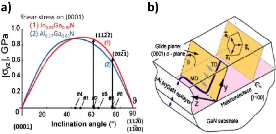
Relaxation processes for c-plane films typically involve formation of V-defects and subsequent local dislocation plasticity in the case of InGaN/GaN films. For semipolar families of planes such as (11-22) and (20-21), the basal plane is inclined with respect to the growth orientation, which results in the presence of substantial shear stresses in lattice-mismatched InGaN and AlGaN films [29]. The stresses depend on the lattice misfit strain and the inclination angle of the semipolar plane. These stresses provide the driving force for formation of misfit dislocations (MDs) by basal plane glide. An example of this is illustrated in figure 2.6.
FIG. 2.6. a) Resolved shear stresses on the basal plane for compressive InGaN and tensile AlGaN films on GaN as function of inclination angle from the basal plane; b) Scheme of misfit dislocation (MD) formation by glide of a pre-existing threading dislocation (TD) for a (11-21) heterostructure [1].
The coherency limits for semiconductor film growth as a function of lattice mismatch were evaluated via the equilibrium approach of Matthews-Blakeslee where the elastic energy in a strained film is compared with the energetics of MD formation by glide. This yields a critical thickness for a film at a given strain and composition beyond which the formation of MDs is energetically favorable compared to maintaining coherency. Such an approach does not take into account the kinetics involved. In the case
22 of III-nitrides, the density of threading dislocations (TDs) is sufficiently high to relax the largest misfit stresses without the need for additional nucleation of dislocations. As a result, the Matthews-Blakeslee limit has been found to be an accurate lower bound for the majority of semipolar III-nitride systems.
The existence of plastic relaxation mechanisms for lattice-mismatched semipolar films has important implications for device design. Two approaches to device design are possible:
1) Design coherent devices making use of theoretical predictions and experimental demonstrations of critical thickness to design and grow heterostructures that will remain fully coherent, ensuring that there is no MD formation.
2) Design metamorphic devices in which a relaxed buffer layer can be used to tailor the lattice constant, to isolate defects from the active region of the device and even to alter the structure of the valence band.
The second approach has been successfully applied to making solar cells, transistors and light emitters based on zincblende III-V materials and has the potential for similar applications to semipolar III-nitride semiconductors [1].
For semipolar InGaN/GaN heterostructures, dislocations in the GaN substrate can propagate into the InGaN/GaN interface and glide in the basal plane to the surface. The layer relaxes along the [10-1-4] direction but remains strained along [-12-10]. As a result, the InGaN layer thickness above which misfit dislocations (MDs) and thus layer tilt occurs is referred to as the critical layer thickness. Macroscopic tilt present in a film is easily detected via symmetric x-ray diffraction (XRD) and the presence of has been confirmed by TEM. Recently, the indium incorporation efficiency and critical layer thickness for MD formation in (20-21) InGaN layers were investigated [30]. InGaN layers with an indium content between 1.7% and 16% were grown by MOVPE. The strain state of the (20-21) layers was determined from x-ray diffraction (XRD) reciprocal space maps (RSM). The indium content and layer thickness were determined from XRD symmetrical θ-2θ scans using the method of Young et al. [31]. The (20-21) layers have been classified as strained, partially relaxed and fully relaxed, according to the amount of tilt in the symmetrical RSM (figure 2.7).
23
FIG. 2.7. Symmetrical (20-21) XRD RSM of a) strained, b) partially relaxed and c) fully relaxed InGaN layers [30].
Partially relaxed layers exhibit a negligible tilt relative to the GaN substrate and have a thickness which might be very close to the critical thickness. The critical thickness value between 55 nm and 110 nm found by Hardy et al. [32] for an indium content of 6% agrees with the observations of Ploch et al. [30]. The critical layer thickness exhibits a behavior as predicted by the Matthews and Blakeslee model, with some deviations. A reduced indium incorporation efficiency was found in comparison to (0001) oriented InGaN layers at growth temperature of 725 °C. The reduced indium incorporation efficiency on (2021) layers in comparison to (0001) layers disagrees with observations made for NH3 MBE growth, where a
higher indium incorporation in (20-21) layers in the growth temperature range between 575 °C and 650 °C was found [33].
It seems that a general statement on the indium incorporation efficiency cannot be made. However, the influence of growth parameters on indium incorporation efficiency remains under investigation.
2.5 Semipolar InGaN LEDs
Group-III nitride based laser diodes and light emitting devices in the visible spectrum employ InGaN quantum wells as active regions.
The standard design for a LED structure is illustrated in figure 2.8. For the LED structure in figure 2.8a, the active region is composed by a InGaN layer surrounded by InGaN barriers. A p-type AlGaN:Mg electron blocking layer (EBL) avoids that electrons diffuse in the p-GaN side, improving the efficiency of the device. This design was developed for LEDs grown on a polar substrate, as well as for semipolar substrates.
24 However, in order to evaluate the polarization fields, the LED structure must be kept as simple as possible, because every heterointerface gives rise to additional fields. Therefore, a second kind of LED structure without the EBL and instead with an InGaN multiple quantum well (MQW) was employed (figure 2.8b). Moreover, the presence of a MQW allows a greater spatial extension of the active region.
FIG. 2.8. Epitaxial structure of two standard LEDs; a) single quantum well structure with electron blocking layer and b) multiple quantum well structure without electron blocking layer [34].
The realization of efficient light emitting devices becomes more difficult with an increasing indium content in the layers. First, the QCSE becomes stronger at higher wavelengths and, second, the incorporation of more indium leads to higher fluctuations of the indium composition in the active region. This fact results in an increase of the line width with increasing emission wavelength in the emission spectra of LEDs.
The emission energy of a QW is mainly determined by the energy gap of the material and by the barrier width, but it can also be affected by the measurement conditions like the sample temperature. The interdependence of indium content, strain and quantum confined stark effect (QCSE) on the emission energy can be very complex. A proper estimation of the different effects is only possible by calculating the QW band structure, taking into account polarization fields and strain and solving the Schrödinger-Poisson equation.
25
FIG. 2.9. Schematic band structure of the active region of a LED [34].
The emission wavelengths of MOVPE grown InGaN QWs were investigated by Wernicke et al. [35] for different crystal orientations with electro luminescence (EL) and photo luminescence (PL). The indium incorporation was estimated by comparison of the emission energies to kp-theory calculations. The normalized emission spectra for InGaN QWs deposited on differently oriented substrates are showed in figure 2.6.
FIG. 2.10. Normalized room-temperature PL and EL emission spectra for c-plane, semipolar and nonpolar InGaN QWs grown at 750 °C [35].
A large variation of the emission energy of almost 600 meV for QWs that were all grown under the same conditions can be observed. A strong variation of the emission energy was observed for InGaN QWs grown at
26 the same temperature of at 750 °C on differently oriented substrates. A clear hierarchy was identified:
(10-11) < (11-22) = (0001) < (20-21) < (10-10) < (10-12)
The comparison between kp-theory and experimental results allow to separate the effect of indium content on the effects of QCSE and strain. The analyses yielded similar indium incorporation efficiencies for (0001), (20-21), (10-12) and (10-10) surfaces. The differences in the emission energy for these orientations can be mainly attributed to the QCSE and the effect of anisotropic strain.
27
Chapter 3
Surface-analytic experimental
techniques
In this chapter, we give an overview on the experimental techniques (listed in table 3.1) used to investigate our semipolar (20-21) InGaN samples. First, we briefly describe the context in which the surface becomes a fundamental physical property and, second, we present the main characteristics of each used experimental surface technique.
The surface of a solid can be very complex. Surface analysis means, in the simplest sense, that the elemental composition of the outermost atom layers of a solid is required. Having found that, there will be immediate requests for detailed knowledge of the chemical binding state, surface reconstructions, surface homogeneity and state of adsorbates. Each of the many surface analysis techniques approaches one or more different aspects better than the others so that, in principle, each has a particular advantage.
Physical property Experimental technique
Symmetry and periodicity Low Energy Electron Diffraction (LEED) Morphology Atomic Force Microscopy (AFM)
Atomic structure Scanning Tunneling Microscopy (STM) Chemical properties and bonds X-ray Photoemission Spectroscopy (XPS) Optical Properties Surface Photovoltage Spectroscopy (SPS)
TAB. 3.1. Experimental techniques used for the investigation of the semipolar (20-21) InGaN samples in this thesis.
3.1 Surface physics
Semiconductor physics cannot be separated from the concept of surface physics. First, the growth of semiconductor materials is realized with techniques which consist in appropriate manipulations of a variety of kinetic processes and chemical reactions which occur at the surface (see section 1.6). Second, the effect of the surface becomes increasingly stronger as the process of miniaturization in the semiconductor technology proceeds. Thus, the study of the surface becomes a fundamental issue, not
28 only for topics of fundamental physics like the transition into the regime of quantum physics, but also for technological purposes. In this sense, the semiconductor research in the last decades has been involved also with topics such as the development of suitable surface preparation methods and the material handling in vacuum conditions.
3.1.1 General considerations
The concept of surface physics is important not only in connection with special experimental tools, but also for certain physical systems. In many theoretical models in the classic solid state physics, the properties of the surface atoms are neglected because their number is several orders of magnitude lower than the number of bulk atoms. However, this condition is no longer satisfied in solid thin films. When probes which are used “strongly” interact with solid matter and penetrate only a couple of Angstroms into the solid, the models of surface physics have to be applied. The same is true for spectroscopic techniques where the particles detected outside the surface originate from excitation processes close to the surface.
A solid interface is defined as a small number of atomic layers that separate two solids in intimate contact with one another, where the properties differ significantly from those of the bulk material it separates. The surface of a solid is a particularly type of interface, at which the solid is in contact with the surrounding world, i.e., the atmosphere or, in the ideal case, the vacuum [21]. The term morphology refers to the macroscopic form or shape of a surface, whereas the structure, on the other hand, denotes the detailed geometrical arrangement of atoms. The distinction between the two terms, however, is sometimes not so clear, even in the case of clean and well-defined surfaces. What we consider as morphology depends on the resolution of the techniques used for its observation. Furthermore, the atomistic structure may often determine, or at least have a significant influence on, the morphology of a surface. It is thus necessary to consider both aspects in the surface analysis of a material.
3.1.2 Ultra high vacuum (UHV)
The word vacuum is used to describe a wide range of conditions. At one extreme, it refers to nearly complete emptiness, i.e. a space in which air and other gases are absent. At the other extreme, vacuum is any gas pressure less than a prevailing pressure in an environment. In each case, the basic property involved is the gas density. Ultra high vacuum (UHV) is a physical condition which requires a pressure of around 10-9 mbar. Furthermore,
29
UHV is not only determined by a pressure condition, but also by a precise chemical condition: air is primarily a nitrogen ambient, whereas UHV is instead a hydrogen ambient. The presence of other minor gases depends on the used vacuum pumps.
The vacuum can be produced by different methods, like mechanical displacement of gases from an enclosed space, chemical reactions which produce solid residues, physical adsorbtion or gas ionization [36]. To produce UHV in a chamber, the evacuation process must start at atmospheric pressure and a sequence of at least two different pumping devices is used. Usually, a rough vacuum level is produce by mechanical pumps and the high vacuum level is developed by diffusion pumps or ion-gettering pumps. The ion getter pumps are mostly used for pressures lower than 10-9 mbar and remain the cleanest and most efficient method to
achieve ultra high vacuum (UHV). The pump captures gases by converting them into solid compounds and binding them inside the pump. Furthermore, ion getter pump operate free of vibrations and agitations at very low power consumption. The ion getter pumps are an integral part of scientific apparatus as particle accelerators, space simulations, mass spectrometers and development and production of semiconductor devices. There are two reasons why electron spectrometers used in surface analysis must operate under vacuum conditions:
1) The mean free path of the emitted electrons should be much greater than the dimensions of the spectrometer. That means that the electrons should meet as few gas molecules as possible on their way to the analyser so they are not scattered and thereby lost.
2) Surface contamination from whatever source should be avoided because every small amount of contaminant can affect the analysis. The sample treatment in UHV requires the preparation of a clean surface. In this context, clean surface is defined as the state of the surface in which the experimental techniques (like XPS and AES) cannot detect characteristic spectral features of impurity elements. The simplest cleaning technique is heat treatment, generally a few hundred Celsius degree below the melting point of the material. The problem is to maintain the cleanliness of the sample on cooling to room temperature, since the temperature will pass through ranges in which impurities segregate quickly to the surface. Another technique used to remove impurities is the ion bombardment, typically with a beam of Ar ions of energy around keV. In some applications and analyses the residual low level of contamination may
30 be acceptable, while in other applications it is necessary to use a combination between more cleaning techniques [37].
3.1.3 Surface preparation
The preparation of semiconductor devices often requires processing in several different atmospheres and, hence, sample transfer between those. During transfer, surface oxidation and other contamination are likely to occur. A minimization of surface contamination is crucial for subsequent device processing as surface defects can govern epitaxial growth and may lead to the formation of bulk defects that cannot be overgrown without substantial effort. This may also lead to deteriorated electronic properties of interfaces. Therefore, the availability of an effective cleaning process of the semiconductor surface after transfer is of crucial importance. Besides oxide formation, the major contaminant on semiconductor surface is residual carbon.
For III-nitride alloys, several cleaning techniques has been tested. It has been demonstrated that thermal annealing, i.e. heat treatment, strongly improves the cleanliness of samples after dry nitrogen transfer and related exposure to residual oxygen. Moreover, plasma assisted cleaning is shown to successfully further remove carbon contaminations [38].
3.2 Electron spectroscopy
Chemical analysis of solid materials with electron spectroscopy is based on energy analysis of secondary electrons that are emitted as a result of excitation by photons, electrons or ions. The main features of the electron spectroscopy techniques are:
1) Detection of all elements except hydrogen and helium 2) Detection of chemical bonding states
3) Information depth in the nanometer range
The reason for the surface specificity of electron spectroscopy is the small information depth of typically some nanometers that is determined by the elastic mean free path of electrons between typically 40 eV and 2500 eV. The most important methods that are employed in commercial surface analytical instruments are X-ray Photoelectron Spectroscopy (XPS) and Auger Electron Spectroscopy (AES). The two techniques are comparable in their surface sensitivity, however peak are analysis in XPS is more accurate than Auger peak to peak height in AES.
31
The most important part of an electron spectrometer is the electron energy analyzer. At present, all commercial photo-electron spectrometers are equipped with a concentric hermispherical analyzer (CHA). The CHA consists of two concentric hemispheres and the outer hemisphere is put on a negative potential against the inner sphere: the mean radius describes an equipotential plane that connects entrance and exit slits. The main purpose of the input lens is retardation of the electrons to reduce their energy before they enter the analyzer. This reduced and constant energy is called pass energy. A CHA spectrometer is shown in figure 3.2.
CHA spectrometers can be operated in two different modes, the constant retard mode (CRR), where ΔE/E is constant, or the constant analyzer mode (CAT), where ΔE is constant. Whereas the CRR mode is generally used in AES, the CAT mode is exclusively used in XPS [39].
3.2.1 X-ray photoelectron spectroscopy (XPS)
XPS is a quantitative spectroscopic technique that measures composition, chemical state and electronic state of the elements that exist within a solid surface. The Photoelectron emission can be imagined as a three-stage process:
1) X-ray interact with the electrons in the atomic shell
2) Photoelectrons are generated and part of these move to the surface after being subject to various scattering processes
3) Electrons reaching the surface are emitted in the vacuum
The kinetic energy of a photoelectron is schematically derived from the energy level scheme shown in figure 3.1. An X-ray with energy hυ generated a vacancy in a core electron level with binding energy Eb. The
emitted photoelectron has to overcome the work function of the sample ΦS. Thus, with reference to the Fermi energy EF, the energy measured by
the analyzer is ( ) kin b S A S b A E h E h E
Because the sample work function is constant and the photoelectron energy is known, the measured photoelectron spectrum is a direct indication of the binding energies of the different atomic electron levels.
32
FIG. 3.1. Scheme of the relevant energy terms in XPS of solid surfaces [39].
A scheme of a typical XPS experimental setup is shown in figure 3.2. The most common X-ray sources used in XPS are equipped with Mg or Al anodes, which exhibit a characteristic Kα radiation of 1253.6 eV and 1486.6
eV, respectively. A thin Al foil of about 2 µm thickness is placed at the exit of the X-rays to shield the sample from stray electrons, from contamination and from the heat. For efficient irradiation, usual sources are operated at (0.5÷1) kW power, at (5÷15) keV anode voltage.
FIG. 3.2. Scheme of a typical XPS experimental setup [39].
The necessity of forced water cooling to remove the heat from the anode also implies that the anode block must be of high heat conductance, which in turn means fabrication of the block and the integral water tubes from copper. Thus, the anode material itself is normally deposited on the copper block as a thick film, typically 10 μm, representing a compromise between being thick enough to exclude copper Lα radiation and thin enough to
33
allow adequate heat transfer [37]. Most of the commercially available X-ray sources have two anode surfaces and it is possible, by simple external switching, to choose one of them. There are two reasons why it is desirable to have a double-anode facility:
1) The two characteristic emission radiations have two different line width allowing two different resolutions
2) The XPS spectrum, both photoelectron and Auger peaks appear, with possible interferences. Since Auger energies are fixed, a change in the X-ray line energy will resolve possible interferences.
For identification of possible differences in chemical states of elements, in XPS it is necessary to apply the same absolute energy resolution to any peak in the spectrum, i.e. at any kinetic energy. It is standard practice to retard the kinetic energies of the electrons either to a chosen analyzer energy, the so-called pass energy. In either case the pass energy is kept fixed during the acquisition of any spectrum. Retardation enables the same absolute resolution to be obtained for a lower relative resolution.
3.2.2 Interpretation of XPS spectra
The XPS technique counts the electron ejected from a sample surface when it is irradiated by X-rays. A spectrum representing the number of electrons recorded at a sequence of energies includes both a contribution from a background signal and also resonance peaks characteristic of the bound states of the electrons in the surface atoms. The resonant peaks above the background are the significant features in typical XPS spectrum, as shown in figure 3.5.
Any change in the bonding state of an atom gives rise to changes in the observed spectral characteristics: binding energy, peak width and shape, valence band changes and sometimes bonding satellites. Chemical bonding in a compound usually causes a change of the binding energy as compared to bonding in the pure element which is called chemical shift. Ignoring final-state effects, the chemical shift can be explained by the effective charge potential change on an atom. For example, when an atom is bonded to another one with higher electronegativity, a charge transfer to the latter occurs and the effective charge of the former becomes positive, thus increasing the binding energy. In practice, references to standard spectra of compound are used to interpret measured chemical shifts [39]. The chemical shifts seen in XPS data are a valuable source of information about
34 the sample. For example, semiconductor surfaces are often covered with an oxide layer: this can be observed in the XPS spectrum as separation between elemental and oxide peak for a given element.
FIG. 3.3. XPS spectrum of a semipolar InGaN sample (own measurement). One can identify the core level peaks N 1s, Ga 3p, In 3d, the surface contaminants C 1s and O and the Ga LMM Auger peak. An inset of the valence band is also illustrated.
The underlying assumption when quantifying XPS spectra is that the number of electrons recorded is proportional to the number of atoms in a given state. XPS spectra are, for the most part, quantified in terms of peak intensities and peak positions. The peak intensities measure how much of a material is at the surface, while the peak positions indicate the elemental and chemical composition [40]. Other values, such as the full width at half maximum are useful indicators of chemical state changes. Broadening of a peak may indicate:
1) Change in the number of chemical bonds 2) Change in the sample condition
3) Differential charging of the surface
Not all the electrons emitted from the sample are recorded by the instrument. The efficiency with which emitted electrons are recorded depends on the kinetic energy of the electrons, which in turn depends on the operating mode of the instrument. So, the best way to compare XPS intensities is via percentage atomic concentrations, i.e. the ratios of the intensity to the total intensity of electrons in the measurement. Should the
35
experimental conditions change between measurements, for example the X-ray gun power output, then the peak intensities will change in an absolute sense, but they will remain constant in relative terms.
The first issue involved with quantifying XPS spectra is identifying those electrons belonging to a given transition. The standard approach is to define an approximation to the background signal. A variety of background algorithms are used to measure the peak. However, none of these algorithms is favored, so that the arbitrariness of the choice represents a source for uncertainty. Peak areas computed from the background subtracted data form the basis for most elemental quantification results form XPS. Relative sensitivity factors of photoelectric peaks are often tabulated and used routinely to scale the measured intensities as part of the atomic concentration calculation. An accuracy of 10% is typically quoted for routinely performed XPS atomic concentrations.
3.2.3 Auger Electron Spectroscopy (AES)
In a typical AES experiment, the sample is irradiated with a focused beam of primary electrons of sufficiently high energy, (1÷20) keV, from the electron gun which penetrate the sample up to a range of the order of (0.1÷1) µm. Auger electrons possess characteristic energies which are well defined by the involved electron levels of the analyzed element [39]. Auger electron emission is imagined as a three-stage process which involves three electron levels:
1) An atom of the sample is ionized by electron impact.
2) The resulting vacancy in a core electron shell will be filled by an electron from a higher level.
3) The excess energy will cause either emission of a characteristic X-ray or emission of another electron, called Auger electron, which leaves the atom with a characteristic energy.
The measured Auger electron energy is given by the difference between the binding energies of the involved electron levels, i.e. referring to figure 3.4 one has
WXY W X Y A
E E E E
By calibration of the analyzer using the elastic peak (with well-defined energy usually at 2 keV), the work function ΦA is removed from this
equation. Reference samples for which standard kinetic energies are available help to establish a correct energy scale.
![FIG. 1.1. Unit cell of III-nitrides with a) zincblende and b) wurtzite crystal structure (top view and side view) [3]](https://thumb-eu.123doks.com/thumbv2/123dokorg/7462242.101784/8.892.135.700.769.986/fig-unit-cell-nitrides-zincblende-wurtzite-crystal-structure.webp)
![FIG. 1.4. Microscopic picture of spontaneous polarization in a free-standing GaN slab [4]](https://thumb-eu.123doks.com/thumbv2/123dokorg/7462242.101784/11.892.212.757.794.1055/fig-microscopic-picture-spontaneous-polarization-free-standing-gan.webp)
![FIG. 1.5. Polarization component along growth direction as function of the angle between growth direction and c-direction for a) AlGaN and b) InGaN on a GaN substrate [6]](https://thumb-eu.123doks.com/thumbv2/123dokorg/7462242.101784/12.892.134.695.660.888/polarization-component-direction-function-direction-direction-ingan-substrate.webp)
![FIG. 1.10. Qualitative picture of the effect of a) substrate temperature and b) reactor pressure on growth rate of the layer [5]](https://thumb-eu.123doks.com/thumbv2/123dokorg/7462242.101784/18.892.218.593.362.884/qualitative-picture-effect-substrate-temperature-reactor-pressure-growth.webp)
![FIG. 2.1. Simple schematic representation of a) relaxation and b) surface reconstruction [21]](https://thumb-eu.123doks.com/thumbv2/123dokorg/7462242.101784/21.892.200.734.205.416/fig-simple-schematic-representation-relaxation-b-surface-reconstruction.webp)
![FIG. 2.5. Model of a semipolar (20-21)-GaN surface [23].](https://thumb-eu.123doks.com/thumbv2/123dokorg/7462242.101784/24.892.151.679.292.519/fig-model-of-semipolar-gan-surface.webp)
![FIG. 2.7. Symmetrical (20-21) XRD RSM of a) strained, b) partially relaxed and c) fully relaxed InGaN layers [30]](https://thumb-eu.123doks.com/thumbv2/123dokorg/7462242.101784/28.892.135.697.127.389/symmetrical-strained-partially-relaxed-fully-relaxed-ingan-layers.webp)
![FIG. 2.9. Schematic band structure of the active region of a LED [34].](https://thumb-eu.123doks.com/thumbv2/123dokorg/7462242.101784/30.892.230.583.133.411/fig-schematic-band-structure-active-region-led.webp)
![FIG. 3.4. Scheme of the optical system able to detect the cantilever bending [42].](https://thumb-eu.123doks.com/thumbv2/123dokorg/7462242.101784/44.892.251.573.319.622/fig-scheme-optical-able-detect-cantilever-bending.webp)
