UNIVERSITA’ DI PISA
Dipartimento di Ingegneria dell’Informazione:
Elettronica, Informatica, Telecomunicazioni
Dottorato di Ricerca in Ingegneria dell’Informazione
Nanopower CMOS transponders for UHF and
microwave RFID systems
Giuseppe De Vita
Tutore: Prof. Giuseppe Iannaccone
Tutore: Prof. Bruno Pellegrini
1. Introduction ...1
1.1. Low-Power electronics ...1
1.1.1. Low-power integrated circuit design techniques...2
Low-power in digital circuits...2
Low-power in analog circuits ...4
1.2. Low-power electronics applications ...7
1.2.1. Wireless sensor networks...7
1.2.2. Ambient Intelligence...9
1.2.3. Implantable medical devices ...10
1.2.4. Radio Frequency IDentification (RFID) Systems ...10
1.3. RFID technology ...11
1.3.1. Brief history of RFID technology ...11
1.3.2. Classification of RFID systems...12
1.3.3. International standards ...14
1.3.4. Passive UHF/Microwave RFID systems...15
1.4. References ...17
2. Design Criteria and Architecture...21
2.1. Introduction ...21
2.2. Voltage Multiplier and Power Matching Network ...23
2.2.1. N-stage Voltage Multiplier ...23
Power Consumption...26
Power consumption in the presence of substrate losses...28
2.2.2. Input Equivalent Impedance ...30
2.2.3. Power Matching Network ...30
2.2.4. Non-Linear Effects...34
2.2.5. Matching when Conditions Vary ...37
2.3. BACKSCATTER MODULATOR...40
2.3.1. ASK and PSK Backscatter Modulation ...40
2.3.2. PSK Backscatter Modulator...44
Circuit description ...45
Comparison with other topologies...47
2.4. Modulation Depth and Maximum Operating Range...49
2.4.1. Transponder input power ...49
2.4.2. Probability of Error at the Reader ...50
Received Signal at the Reader’s Antenna...50
Receiver Architecture ...51
Noise Spectral Density ...53
2.5. References ...58
3. Voltage Reference...60
3.1. Introduction ...60
3.2. Overview of CMOS-Based Voltage Reference ...61
3.3. Proposed Voltage Reference 1...63
3.3.1. Operating Principle of the Proposed Reference Voltage Generator63 3.3.2. Circuit Description...65
Current Generator Circuit ...65
Active Load ...67
3.3.5. Line Sensitivity ...71
3.3.6. Experimental Results ...71
3.4. Proposed Voltage Reference 2...73
3.4.1. Circuit Description...73
3.4.2. Temperature Compensation ...75
3.4.3. Second order effects on the temperature coefficient ...76
Channel length modulation effect...76
3.4.4. Body effect...77
3.4.5. Power Supply Rejection Ratio ...78
3.4.6. Experimental Results ...81
3.5. Proposed Voltage Reference 3...83
3.5.1. Circuit Description...83
Current generator circuit...84
Active load...85
3.5.2. Design Consideration...86
Channel length modulation effect...86
Minimum power consumption dimensioning ...86
Sensitivity to process variations ...87
3.5.3. Dynamic Range...87
3.5.4. Temperature Compensation ...88
3.5.5. Second order effects on the temperature coefficient ...88
Channel length modulation effect...88
Body effect ...90 3.5.6. Experimental Results ...90 3.6. Conclusion...94 3.7. References ...95 4. Power Supply ...97 4.1. Introduction ...97
4.2. Architecture of a Passive RFID Transponder ...98
4.3. Temperature compensated voltage regulator ...100
4.3.1. Circuit description...100
4.3.2. Temperature Coefficient ...102
4.3.3. Experimental Results ...104
4.4. Negative-Temperature coefficient voltage regulator ...104
4.4.1. Series Voltage Regulator...107
4.4.2. Supply Voltage Range...109
4.4.3. Temperature Coefficient ...110
4.4.4. Experimental Results ...112
4.5. Constant-delay voltage regulator...116
4.5.1. Current Reference Circuit ...116
4.5.2. Voltage Reference Generator...118
4.5.3. Sensitivity to Temperature Variations...119
4.5.4. Sensitivity to Process Variations...120
4.5.5. Experimental Results ...121
4.6. Conclusion...125
4.7. References ...125
5.2. Memory Costraints ...129
5.3. Memory Cell...129
5.4. Memory Architecture ...132
5.5. Memory Circuits...132
5.5.1. Sense Amplifier...132
5.5.2. Word Line Driver...134
5.5.3. Input and Output buffer and Y decoder...137
5.6. Experimental Results...137
5.7. Conclusion...143
5.8. References ...143
6. Complete implementation of a passive transponder...145
6.1. Transponder architecture ...145
6.2. Analog section ...146
6.2.1. Voltage multiplier ...147
6.2.2. Demodulator...149
6.2.3. ASK backscatter modulator ...150
6.3. Digital section...152
6.3.1. Random delay ...153
6.3.2. Acknowledgement detector...153
6.3.3. Clock generator ...154
Circuit Description...155
Current Reference Generator ...156
Voltage Reference ...157
Temperature Coefficient...158
Process Variations Sensitivity ...158
Simulation Results ...159
6.4. Conclusion...162
6.5. System performance ...163
6.6. References ...163
1.
I
NTRODUCTION
1.1. Low-Power electronics
Low-voltage and low-power integrated circuits design techniques were originally developed, more than 30 years ago, for wrist watches. The power consumption of quartz-crystal wrist watches must be smaller than few μW to ensure a sufficient duration of the available energy source. In quartz-crystal wristwatches it is preferable to work at high input frequency so that quartz crystals are cheaper and have a better temperature coefficient. In such condition, we thus need a frequency divider to generate the 1 Hz-clock signal required for the correct operation of the watch. As a consequence, it is very important to reduce as much as possible the dynamic power of the first dividing stages, which work at higher frequency. In the literature it is possible to find different works where some solutions for low-power frequency dividers are proposed [1], [2], [3]. In the design proposed in [3], at a supply voltage of 1.35 V the maximum frequency is 2 MHz and the dynamic power consumption per stage is 1.6 nW/kHz, which is one order of magnitude smaller than that of the designs proposed in [1], [2]. These are the first examples of low-power and low-voltage integrated circuits. Today, wrist watches have a complexity larger than some thousands of transistors with an on-board microcontroller and they have a power consumption smaller than 0.5 μW at supply voltages smaller than 1.5 V.
In recent years, in virtue of the widespread diffusion of battery-operated devices, especially in the field of medical applications and short-range low frequency communication, there is a growing demand for low-power circuits. In such systems the low-power consumption is the first requirement, whereas other requirements, such as speed or dynamic range, are sacrificed. In battery-operated systems, the demand for low-power circuits is driven by the need to extend the battery life time, in order to reduce the replacing or recharging procedures, which often are very costly, as in the case of sensors or identification devices distributed in a wide area, or difficult to perform, as in the case of medical implantable devices. In such applications, there is also a stringent requirement for small size and weight and this imposes to use small-size batteries, which thus are able to provide quite small energy capacity (few Wh). In many applications scenario, the targeted node lifetime ranges is typically between 2 to 10 years, which sets a drastic requirement on the power consumption. Indeed, in the case of an on-board 1.5 V-AA-battery of 2.6 Ah with a leakage current of 30 μA, in order to achieve a lifetime lying between 2 to 7 years, an average power consumption comprised between 10 to 100 μW is required. Since the power consumption of radio transceivers commercially available today
ranges typically in the several tens of mW, for example a Bluetooth transceiver consumes some tens of mW [4], [5], it is clear that there is the need to develop ad-hoc circuits with very low power consumption.
Moreover, in recent years, in most of VLSI-based systems, including computers and telecommunication products, the urgent need of portability and the growing relative cost of power supplies and heat-removal systems are leading to a strong demand for low-power circuits [6], [7], whereas, until few years ago, the power consumption was the least important requirement and the largest interest was in achieving higher and higher speed and precision. High power consumption in modern VLSI systems causes self-heating, which is a big problem because, when the chip temperature increases, there is a strong reduction of the device reliability and a degradation of the system performance. As a consequence, in order to ensure a safe and high-performance operation, cheap plastic packages can not be used anymore but it is necessary to use air-cooled packages or other kinds of packages, which are much more expensive. Moreover, in order to satisfy the increasing need of power in high performance portable systems, such as laptop and mobile phones, more and more expensive batteries are developed, to provide the power required with a life time long enough. Their cost is, by now, a large fraction of the total cost of the product in which they are installed.. As a consequence, today, the low-power trend in circuit design is mainly driven by two forces: on the one hand, the demand for long-life battery-operated systems and, on the other hand, the technological limitation of high performance VLSI systems. In the last years, the strong demand for low-power consumption has led to the development and use of several techniques, both for digital and analog circuits.
1.1.1. Low-power integrated circuit design techniques
As far as low-power design techniques are concerned, it is usually convenient to distinguish between digital and analog circuits.
Low-power in digital circuits
The power consumption in VLSI digital circuit can be written as,
P=12CVDDΔVf +IstVDD+IstaticVDD, ( 1-1 )
where VDD is the supply voltage, C is the load capacitance, ΔV is the load voltage
swing, f is the load switching frequency, Ist is the shortcircuit current and Istatic is the
static current due to junction currents, subthreshold currents and gate tunneling currents. The first term is the load switching power, the second term is the shoot through power and the third term is the static power. Several techniques have been developed to reduce each of the three terms.
The load switching power can be drastically reduced through minimization of capacitance, voltage and frequency. The capacitance minimization can be achieved by a power/performance sizing, clock-gating strategies and glitch suppression
procedures. It is clear that the largest capacitances in the chip are the output capacitances due to pads and package and then most of the switching power is consumed to charge/discharge such capacitances. Usually, in order to drive such capacitances, a sizing, based on the gate size multiplier in an exponential horn of inverters, is used. Unfortunately, such strategy is optimized to maximize the performance in term of speed. Device sizing for power efficiency is significantly different than sizing for performance and then a proper strategy, optimized for power efficiency, must be used achieving a good trade-off between power and performance [8]. A final solution to minimize the output capacitances, which are power hungry, is to use System on Chip (SoC): the integration in a unique chip totally eliminates such capacitances. In VLSI systems, from 25% to 50% of power consumption is usually due to driving latches, most of which have a low utilization (10-35%). In order to reduce the power consumption, a strategy is to gate-off unused latches and associated logic, turning off clocks to unused units or to individual latch banks [9]. Glitches can represent a significant portion of the dynamic power and they can be avoided by using non-glitching logic, such as domino, and by a careful timing dimensioning in order to adjust the delays in a proper way [10].
The voltage minimization can be achieved by lowering the voltage swing and the supply voltage. The most efficient strategy, in this sense, is to lower the supply to lower both VDD and ΔV. The supply voltage reduction is the most promising
strategy to drastically reduce the power consumption in modern VLSI systems. Indeed, the maximum frequency is proportional to the supply voltage ( f ∝VDD)
but the power is proportional to 3
DD
V and then, when reducing the supply voltage, the power consumption is drastically reduced while the performance is still acceptable.
Lowering the frequency allows us to reduce the power linearly but does not improve the energy efficiency. Anyway, such solution is important to avoid heating problems.
The shoot through power can represent a not negligible portion of the dynamic power consumption (8-15%). It can be minimized by lowering the supply voltage or by avoiding slow input signal, in order to minimize the time interval during which both the pull-up and pull-down network of the driven gate are enabled simultaneously.
The static power consumption can be minimized by lowering the supply voltage or by lowering the static currents. In this sense, NMOS, pseudo-NMOS or CMOS CML logics must be avoided, except for very specialized applications. In modern sub-micron IC technologies the gate tunneling current, because of the low oxide thickness, is the most important component of the static current in VLSI systems and is the major power issue especially for the standby power. Since tunnel current is exponentially dependent on the electric field in the oxide [11], a reduction technique consists of reducing the supply voltage, in order to reduce the voltage
across the oxide, or of using new gate materials with higher dielectric constant, in order to increase the equivalent oxide thickness [12]. Both solutions lead to a strong reduction of the tunneling current through the oxide. As a consequence, lowering the supply voltage has a double effect in reducing the stand-by power because it reduces both VDD and Istatic. The subthreshold current, instead, is quite significant in
fast low-threshold voltage devices. An approach is to use low-threshold voltage devices only in the critical paths, to guarantee high performance, and to use high-threshold voltage devices in the rest of the system, to drastically reduce the subthreshold current [13], [14]. Another possibility to reduce subthreshold current is to use stacked devices [15]. Especially for energy constrained systems, such as battery operated systems, the stand-by power can be drastically reduced by two levels of supply gating: to lower or to turn off power supply to the whole system when inactive and to turn off inactive units while system is active.
In conclusion, some trade-offs must be faced. In order to achieve high performance, we need high supply voltage and low threshold voltage to minimize the propagation delay; in order to minimize dynamic power we need low supply voltage and low threshold voltage; in order to minimize stand-by power we need low supply voltage and high threshold voltage. A trade-off must be found according to the specific application we are interested to.
Power reduction must be also performed at the architectural level through the development of ad-hoc domain-specific computing architectures because general purpose microprocessors can dissipate 500 times more power than an ad-hoc hardware realization [16]. Since most of the power is dissipated for data transfers to the memory, cache and local registers, different methods have been proposed for a better utilization of memory hierarchy and processor cycles [17] and to design optimal memory architectures for low power [18]. Such techniques consist of proper transformations of the code to reduce memory accesses to external memory, to improve data locality in the on-chip cache and to optimize the storage order to reduce address computation. Such transformations drastically reduce the total number of accesses to memory leading to a strong power reduction. Another way to reduce the power consumption is to lower as much as possible the clock frequency by exploiting parallelism. Indeed, in an Ambient Intelligence platform there are many concurrent tasks with different sampling rate and then the best choice is to use a multi-processor architecture with its own localized memory where each processor is optimized for the addressed application with a specialized instruction set and with the minimum allowable clock speed.
Low-power in analog circuits
While in digital circuits the most efficient way to drastically reduce the power consumption is to reduce the supply voltage, in analog circuits the low-power techniques are quite different. In analog circuits, lowering the supply voltage does not automatically reduce power consumption. Indeed, the power consumption of
analog circuits is basically set by the Signal to Noise Ratio (SNR) and the operation frequency, and its minimum value is independent of the supply voltage. In analog circuits the power is dissipated to keep the energy of the signal larger than the thermal energy. Let us consider a 100% current efficient single pole transconductor used to charge and discharge an output capacitance. The power P, drawn from the supply voltage VDD, to have a sinusoidal voltage across the capacitance C with a
peak-to-peak value VPP isCfVPP
(
VDD/VPP)
2 . The output noise power is kT / , C where k is the Boltzmann’s constant and T is the absolute temperature. As a consequence the signal-to-noise ratio is,
C kT V SNR PP / 8 / 2 = . ( 1-2 ) Then we can write,
P=8kTf(SNR)VDD/VPP. ( 1-3 )
For a given SNR and frequency, the minimum power consumption to realize a single pole is achieved for VPP =VDD, and then the minimum power consumption is
independent of the supply voltage [19], [20]. From such consideration, it is clear that power efficiency circuits must be designed to be rail-to-rail. Such power limit can be applied at each pole of any linear analog circuit and it is very stringent because it requires a factor 10 of power increase every 10 dB of SNR increase. As a consequence, analog circuits become very power inefficient, in the case of systems that require very large SNR. Such considerations do not depend on the technology or on the supply voltage.
Such theoretical lower limit to the power consumption is increased by other technological limitations in practical circuits’ implementations. For example the power dissipated in bias circuitry is wasted and, in addition, if the bias schemes are inadequate, they can increase the noise and then a larger power is required. Since the minimum power consumption is achieved for a voltage swing equal to the supply voltage, it is important that the signal is amplified as early as possible to its maximum value and maintained along the signal path.
Another aspect to be considered is the presence of additional noise sources, such as those internal to active and passive components or the noise coming from the supply voltage, which forces to increase the power consumption to maintain a given
SNR. Another aspect that leads to an increase in the power is the need for precision,
which imposes to use larger dimensions for active and passive components causing an increase of parasitic capacitances and then of the power. In the case of switched capacitors, the clock frequency must be at least twice as large as the maximum frequency of the signal and then the power consumed by the clock could be dominant. Different techniques exist to reduce the effect of such limitations by acting at circuit or device level.
Although in analog circuits the minimum power for a given SNR and frequency does not depend on the supply voltage, because of the technological limits described above, such as the power dissipated in the bias circuitry or the fact that the voltage swing is not equal to the supply voltage, the power dissipated in an analog circuit slightly depends on the supply voltage. The trend in modern CMOS technologies is to reduce the supply voltage, especially to accomplish the power requirement of digital circuits. In micropower analog circuits the use of MOS transistors in weak inversion provides several advantages for power and low-voltage purposes, as will be explained in detail in the following. An important aspect for low-voltage applications is that the drain-source saturation voltage in the weak inversion operation is much smaller than that in strong inversion, since it is sufficient that the drain-source voltage is larger than the thermal voltage; this helps to reduce the supply voltage. Moreover, in the weak inversion the transconductance-to-current ratio of a MOS transistor reaches its maximum value, approaching that of a bipolar transistor. Indeed, the I-V characteristics of a MOS in the saturation and in the weak inversion regions can be well approximated by,
(
)
2(
)
2 2 2 GS th GS th ox D V V k V V L W C I = μ − = − , ( 1-4 ) ⎥ ⎥ ⎦ ⎤ ⎢ ⎢ ⎣ ⎡ ⎟⎟ ⎠ ⎞ ⎜⎜ ⎝ ⎛ − − ⎟⎟ ⎠ ⎞ ⎜⎜ ⎝ ⎛ − = T DS T th GS T ox D V V mV V V L W V C I μ 2 exp 1 exp , ( 1-5 )where µ is the carrier mobility in the channel, VT is the thermal voltage, Vth is the
threshold voltage, m is the subthreshold slope parameter, W and L are the channel width and length, respectively. As a consequence the transconductance-to-current ratio of a MOS transistor in the saturation and in the weak inversion are given by
(
VGS −Vth)
/2 and1/
(
mVT)
, respectively. Since VT <(
VGS −Vth)
, thetransconductance-to-current ratio of a MOS transistor in the weak inversion is larger than that of a MOS in strong inversion. As a consequence, when the current is limited, weak inversion provides maximum gain-bandwidth product for a given load capacitance or minimum input equivalent noise for a given output noise. Moreover, weak inversion also provides maximum gain per device and minimum input referred offset in a differential pair.
On the other hand, the maximum value of the transconductance-to-current ratio of a MOS transistor leads to a maximum mismatch of current mirrors. Indeed, the current mismatch ΔID due to the threshold voltage mismatch ΔVth is given by
th m
D g V
I = Δ
Δ and then, for a given current, a maximum mismatch is achieved in the weak inversion. Moreover, in the weak inversion the device has a higher noise. Indeed, the drain current noise has a spectral density given by 4kTγ (where gg0 0 is
current, maximum noise is achieved. As a consequence, in low-voltage current mirrors a trade-off must be found between, on the one hand, low voltage operation and, on the other hand, worse precision and higher noise. The other drawback of MOS transistors in weak inversion is that the transition frequency does not exceed a few hundreds of MHz and that they can not be used in high-frequency analog applications. In the strong inversion region, the transition frequency of MOS transistors increases to some GHz but the power consumption becomes higher, as previously explained. For such reason, BiCMOS is the best technology for low-power and high-frequency analog circuits.
In order to reduce power consumption in analog circuits, some techniques at the system level can be adopted. In analog circuits, the limit of the minimum power calculated in ( 1-3 ) can not be overcome and, usually, at least ten times more power will be needed for practical reason. This means that it is not possible to implement a 16-bit audio A/D converter (SNR = 98 dB) with a power consumption smaller than 50-100 μW and other power will be needed to amplify the signal after the conversion. A few microwatts per pole will be sufficient for the subsequent signal processing. As a consequence, most of the power in signal processing chain is consumed in the analog interfaces when the dynamic range is smaller than SNR. Some power reduction technique can be used if the SNR is much smaller than the dynamic range, as in the case of hearing aids where the speech transmission requires a SNR of only 40 dB but a dynamic range larger than 100 dB. In such cases, power can be reduced by maintaining the SNR at its minimum value, independently of the signal, and the dynamic range at the required value. This means that, if the signal is weak, the noise floor must be low and, if the signal is large, noise floor must be raised to achieve the required SNR. This can be achieved by using analog floating point technique, which basically consists in dividing the input signal by a proper factor so that the signal fits within a given range [22]. In such a way, the signal that enters the processor is always within a min-max range and then the SNR is always kept constant. Such technique well fits with switched-capacitor circuits in which the updating can take place between two sampling instants.
1.2. Low-power electronics applications
1.2.1. Wireless sensor networks
A network of wireless sensors consists of a large number of energy-autonomous microsensors distributed in an area of interest. Each node monitors its local environment, locally processes and stores the collected data so it can be used by other nodes. It shares this information with the other neighboring nodes by using a wireless link. Specific features of interest to the end-user can be extracted from the
different information collected by several nodes. The wireless sensor networks can be used for several applications in the field of logistics, identification, medical applications, industrial control, etc..
Many applications can be thought in the field of logistics, asset tracking and supply chain management [23]. For example, the wireless sensor networks can be used to solve the problem of tracking container in a large port [24]. In a port there are thousands of containers stacked one on the other and some of them are empty, others are bound for many destinations. To improve the efficiency is necessary that the location of each container is known exactly that it is chosen so that the containers next needed are close to the ship, where they have to be loaded, and are on the top of the stack. The use of a sensor networks with a sensor on each container allows us to determine the position of each container. In the same way, the wireless sensor network can be used in the supply chain management to know the precise location of an item in a large warehouse. This means that it is possible to know the location of an item to be sold or to perform an automatic inventory, drastically reducing the costs.
Another application of wireless sensor network is for health monitoring, such as athletic performance monitoring to store pulse and respiration rate information and to send such information to a personal computer for later analysis, or daily blood sugar monitoring to record blood sugar values. Wireless sensor networks in health monitoring are expected to extend their field of applications to monitor some enzymes or other biological materials.
Several features distinguish the wireless sensor networks from other standard wireless network. The first one is the size. The nodes must be smaller than one cubic centimeter and less than 100 grams so that they can be embedded into the environment. Second, each node must be low-cost to enable the realization of sensor networks with a large number of nodes. This means that the single node, the communication protocol and the network design must have low complexity to satisfy the low-cost requirement. The most critical issue is the stringent power requirement, which requires a node’s power consumption smaller than 100 μW [25]. Indeed, nodes are typically battery-operated and, since the nodes are many and they might be deployed in hardly accessible regions, they should not require any maintenance. The nodes have therefore to be energetically autonomous and hence the batteries can not be replaced or recharged. The last few years have seen the emergence of numerous new radio technologies. The trend in these technologies is to offer higher and higher data rates to enable the consumers to transfer larger quantity of data in smaller time. Anyway, such high-data-rate technologies do not address the low-end classes of application, which do not require such high speed and complexity. Among wireless commercial devices available today, the closest match is the Bluetooth transceiver, which consumes more than some tens of mWs and costs more than 10 dollars [4], [5]. Such performance, in terms of power and cost, is orders of magnitude above that required for wireless sensor networks. To reach this stringent power requirement the operating range of each node is limited
to a few meters and the data-rate is limited to a few kbps. Anyway, energy optimization must be performed at each level of the system design process, from the physical layer to the communication protocol.
1.2.2. Ambient Intelligence
In the near future, cars, offices and houses will have a distributed network of intelligent devices that provide information, communication and entertainment. These systems will adapt to the user in a context-aware fashion and will differ substantially from contemporary equipment in their appearance in people’s environments and in the way users interact with them. Ambient intelligence is the term used to denote such paradigm. Ambient Intelligence refers to the presence of an environment that is sensitive, adaptive and responsive to the presence of people or objects [26], [27]. In a car environment, Ambient Intelligence can serve, for example, the purpose of safety improvements, intelligent navigation and comfort enhancement. In an office environment, Ambient Intelligence will serve productivity enhancement by supporting the office workers and by improving their living conditions. As an example of application, we can consider the management of environmental control systems in large office buildings. Distributed sensors and actuators allow us to monitor and control some environmental parameters, such as temperature, airflow, light, etc., improving the living conditions of the occupants by, for example, giving the possibility to create micro-climates according to occupants’ preferences. Moreover, the wireless solution eliminates the costs of wires and of installing wiring for a single sensor. In a home environment, Ambient Intelligence will improve the quality of life by creating the desired atmosphere and functionality via intelligent, personalized inter-connected systems and services. It is possible to think at a remote control that can control all home electronic equipments, such as the television, DVD player, stereo, washing machine, but also the lights, the curtains, the locks, etc.; then, an intelligent system can offer some services, such as closing the curtain when the television is turned on, or automatically muting the television when a call is received. To make Ambient Intelligence a reality, many innovations have to be realized, both in hardware and software. An Ambient Intelligence system exhibits a multitude of environment-system interfaces (sensors, actuators and transducers), handling the complete conversion between external information sources/sinks and the digital signal processing world, consisting of a sensor/actuator/transducer combined with RF and mixed signal circuits. Low-data rate sensors and actuator control signals form the interface between environment and system with data rates as low as 1 b/s or less. One of the challenges is to find power- and cost-optimized solutions at very low-data-rate, both wireless and wired. For a radio technology to succeed in the Ambient Intelligence applications, it must take into account the driving factors of all applications areas, such as extremely low-cost, ease of installation, short-range operation and reasonable battery life. Also for Ambient Intelligence applications,
there is the stringent need to develop wireless devices with a low complexity, to ensure low-cost, and with a very low-power consumption.
1.2.3. Implantable medical devices
Implantable medical devices (IMDs) are used in the treatment of many diseases, including heart diseases, neurological disorders and deafness [28]. IMDs are widely used in the treatment of arrhythmias, which is a condition of heart rhythm problems that occurs when the electrical impulses that coordinate heartbeats do not function properly, causing the heart to beat too fast, too slow or irregularly; such heart disease is treated by the use of pacemakers and Implantable Cardioverter Defibrillators (ICDs) [29], [30], [31], which guarantee the correct heartbeats. Another application field of IMDs is for the treatment of hearing loss [32]. A hearing aid is an electronic, battery-operated device that amplifies and modifies sound to allow for improved communication. Hearing aids receive sound through a microphone, which traduces the sound waves to electrical signals. The audio signal is amplified and sent to a loudspeaker. New ultra-low-power radio frequency technologies are spurring the development of innovative medical tools, from endoscopic camera capsules to implanted devices that wirelessly transmit patient health data. The most important requirement of IMDs is the very low power consumption required to extend the battery life time to several years since such devices are implanted and battery replacement is very difficult. Indeed, implanted battery power is limited and the impedance of the battery is relatively high, limiting peak currents that may be drawn from the supply (< 6 mA). The transceiver must operate in a low-power sleep mode, with an extremely low current (< 1 μA), and with the capability to look periodically for a wake up signal..
1.2.4. Radio Frequency IDentification (RFID) Systems
In recent years, automatic identification procedures have become very popular in many service industries, purchasing and distribution logistic operations, manufacturing companies and material flow systems. Automatic identification procedures are used to provide information about people, animals, goods and products in transit. In RFID systems, the transfer of power and data from the reader to the transponder and viceversa is performed using radio communication. Also in such kind of applications, the power requirements in the design of the transponder is very critical, in order to extend the battery life time, in the case of an active transponder, or to extend the operating range, in the case of a passive transponder.
To meet the requirements of the applications within IMDs, wireless sensor networks, ambient intelligence, RFID systems, a successful design must have several specific features: extreme low-power, low-cost, low data-rate. The need for these features leads to a combination of interesting technical issues not found in other widespread wireless network technologies, such as Bluetooth, IEEE 802.11.
1.3. RFID technology
Radio Frequency Identification (RFID) technology proposes new solutions to replace the traditional automatic identification systems, such as those based on barcodes and smart cards. An RFID system consists of an ensemble of transponders, each applied to the objects to be identified, and a reader that interrogates the transponders via radio waves, [33]. In a barcode system, in order to read the information the barcode must be brought rather close to the reader (few tens of cm) and in visual line of sight. Moreover, although the bar code is very cheap, it has a very low storage capacity and it can not be reprogrammed.
A more flexible solution is to store the information in a silicon chip. The most common way of electronic data-carrying device in use in everyday life is the smart card based on contact operation. However, the mechanical contact used in smart card is often impractical. In RFID systems, instead, a contactless transfer of data between the data-carrying device and the reader is performed via radiowaves. A transponder can be identified in a unique way by an identification code stored in the transponder. In principle, the silicon chip can store a large amount of information that can be read and written at a distance of several meters.
1.3.1. Brief history of RFID technology
The origin of RFID systems can be traced back to the World War II. In that period, exactly in 1935, Watson-Watt had been discovered the radar but there was the problem that the radar was able to warn of approaching planes but not to distinguish if the planes belonged to enemies or not. In order to solve such problem, the British introduced the first example of tag, which was installed on each plane; such tag, when the plane was approaching at the airport, received a signal from the radar stations and answered by transmitting a signal to identify the plane as friendly. This was the first example of transponder and in the following years a larger and larger number of scientists were involved in the research dealing with the identification by exploiting the RF energy [34], [35], [36]. The first example of commercial use of RFID system was the Electronic Article Surveillance systems, which employs 1-bit transponders, that can be set on or off according to if the item was paid or not.
The first patent for an RFID system was received by Mario W. Cardullo on January 23th, 1973 [37]. In the mid-1980s, an RFID system was commercialized for automatic toll payment: a transponder was installed on a car or truck and a reader at the gates. Such system was widely used for the automatic toll payment of roads, tunnels and bridge. In the same years, under the request of the US Agricultural Department, a passive RFID system at 125 kHz was developed for the identification of cows [38] and they are still currently used for the same purposes. Later, passive low-frequency transponders were also used for access control to buildings.
In the following years, RFID systems operating at higher frequencies were introduced to achieve larger operating ranges and larger bandwidth. At first, RFID systems at 13.56 MHz were used for access control, automatic toll payment and in contactless smart card. In 1990s, IBM introduced the first UHF RFID system, which was able to provide an operating range larger than 6 meters, and it was used in several applications, especially in the supply chain management [39]. But the technology was expensive at the time due to the low volume of sales and the lack of open, international standards. UHF RFID had an important boost in 1999, when the Uniform Code Council, EAN International, Procter & Gamble and Gillette created the Auto-ID Center at the Massachusetts Institute of Technology. The objective of the Auto-ID Center was to develop low-cost RFID tags by putting only a serial number on the tag to keep the price down so that they could be applied on all products to track them through the supply chain. Then the serial number on the tag was read and stored in a database that would be accessible over the Internet. Previously, tags were a mobile database that carried information about the product or container they were on with them as they traveled. Now, RFIDs were turned into a networking technology by linking objects to the Internet through the tag.
In recent years automatic identification procedures have become very popular in many service industries, purchasing and distribution logistics industry, manufacturing companies and material flow systems. Some of the biggest retailers in the world – Albertsons, Metro, Target, Tesco, Wal-Mart- and the U.S. Department of Defense have said they plan to use RFID technologies to track goods in their supply chain [40],[41], [42], [43], [44].
The number of companies actively involved in the development and sale of RFID systems indicates that this market that should be taken seriously. Whereas global sales of RFID systems were approximately 900 million of dollars in the year 2000 it is estimated that, over the next five years, the market grows at a compound annual growth rate of almost 30%, reaching $1.18 billion in 2010 [45]. The RFID market therefore belongs to the fastest growing sector of the radio technology industry, including mobile phones and cordless telephones [46].
1.3.2. Classification of RFID systems
We can introduce different kinds of classification according to the feature we are considering.
An important feature of RFID systems is the power supply to the transponder. According to such aspect, transponders can be classified as passive or active. Passive transponders do not have an on-board battery and then all the power required to supply the transponder and to transmit data to the reader is generated by rectifying the RF power transmitted by the reader. Active transponders, instead, have an on-board battery to supply all or part (semi-passive) of the power required by the transponder.
The most important differentiation criterion for RFID systems is the physical coupling method, which strongly affects the achievable operating range. It is
possible to distinguish three different coupling methods, i.e. inductive coupling, electrical coupling and electromagnetic coupling. Each of them exploits a different physical principle and then can operate at different frequencies and can achieve different operating range.
Most RFID systems exploit the inductive coupling to transfer power and data between the reader and the transponder. In such systems, the coupling element is a coil that acts as antenna. Inductive-coupled transponders are almost always passive and then they draw the energy required for their operation by the reader. The reader coil generates a magnetic field that in part concatenates with the transponder’s coil and an alternating voltage is generated at the transponder coil terminals. Such voltage is then rectified to generate the DC power required for the operation of the transponder. Usually, in order to boost the voltage generated at the transponder coil terminals, a capacitor is added in parallel with the antenna coil to create a resonant circuit at the transmission frequency of the tag-reader systems. The inductive coupling systems thus exploit the transformer-type coupling between the primary coil in the reader and the secondary coil in the transponders. In order to have such type of coupling, the transponder must be located in the near field of the transmitter coil antenna, that is the distance between the coils must be smaller than 0.16 λ, where λ is the wavelength associated to the transmission frequency. For such reason, inductive coupling systems can not operate at very high frequency otherwise the operating range would be drastically reduced. Since the efficiency of power transfer between the two coils is proportional to the operating frequency, the number of windings and their area, for a given efficiency, the higher the operating frequency of the RFID systems and the smaller is the size of the antenna coils in the reader and the transponder [33]. As a consequence, a trade-off must be found between operating range and sizes. They typically operate at 135 kHz or 13.56 MHz and the operating range is smaller than 1 m.
In electrically coupled RFID systems, the coupling element consists of a large metal plate, which acts as an electrode, and they typically are passive. By applying an alternating voltage at the reader’s electrode, an alternating electrical field is generated which couples with the transponder’s electrode, allowing power transfer from the reader to the transponder. Also in this case, a resonant circuit is created in the transponder to step up the voltage generated at the transponder’s terminals. In order to ensure the capacitive coupling, the electrodes of transponder and reader must be close to each other. For such reason, such systems typically have operating range of few centimeters.
In electromagnetic coupled RFID systems, the coupling element is an antenna, which typically is a dipole or a patch antenna. They usually exploit an electromagnetic coupling in the UHF (868 MHz in Europe and 916 MHz in USA) or microwave range (2.45 GHz or 5.8 GHz). Such systems can achieve an operating range of few meters, in the case of passive transponder, and larger than 15 m, in the case of active transponder. The main advantage is the possibility to achieve a higher operating range, which is required for the adoption of RFID systems in many
logistics and tracking applications. Moreover, since such systems have a high carrier frequency they can have a large bandwidth that allows transmission of large data volumes. Since the size of the coupling element is proportional to the wavelength, electromagnetic RFID systems can have smaller size than that of inductive coupling RFID systems.
Furthermore, passive RFID systems with electromagnetic coupling allow one to achieve operating ranges of some meters with no battery to be maintained. . The widespread adoption of passive electromagnetic coupling RFID systems strictly depends upon the possibility of extending the operating range to several meters by drastically reducing the power consumption of a transponder.
Another classification is done according to the possibility of writing information in the transponder. In read-only transponders, the identification code is set at the fabrication and it can not be modified anymore. Writeable transponders, instead, have an embedded EEPROM memory where the identification code and additional information is stored.
1.3.3. International standards
An important issue, which limits the widespread adoption of RFID systems, is that too many different standards still exist, i.e. EPC, several ISO standards, and proprietary standards. Such standards specify the communication protocol and parameters for air interface. The EPC standard was developed by Auto-ID Center and it is currently managed by EPC Global. EPC currently includes three different standards for RFID systems:
Class 0 for UHF RFID transponder [47];
Class 1 for 13.56 MHz- and UHF- RFID systems [48]; Class 1 Gen 2 for UHF RFID systems [49].
ISO is the International Standardization Organization has developed many standards for RFID systems according to the application they are using for. The standard ISO 18000 is one of the most widely adopted. It defines the parameters for air interface of transponders and it is divided into 7 parts according to the operation frequency of the RFID systems. More in detail, we have,
ISO 18000-1: generic parameters of air interface [50]; ISO 18000-2: parameters for air interface < 135 kHz [51]; ISO 18000-3: parameters for air interface at 13.56 MHz [52]; ISO 18000-4: parameters for air interface at 2.45 GHz [53]; ISO 18000-5: parameters for air interface at 5.8 GHz [54]; ISO 18000-6: parameters for air interface at 860-930 MHz [55]; ISO 18000-7: parameters for air interface at 433.92 MHz [56].
Besides such standards that define the communication protocol and air interface parameters we have also to mention the standard that defines frequency, power and channels that can be used without interfere with other existing communication standards. In Europe, in September 2004, ETSI defined the standard ETSI EN 302
208-1 that fixes at 2 W the maximum power level that can be transmitted by Radio Frequency Identification equipment operating in the band 865 MHz to 868 MHz [57]. Anyway, Italy is one of the last countries in Europe that has not adopted such standard yet. Indeed, Italy still adopts ERC/REC Recommendation 70-03, which, according to the national restrictions, fixes the maximum power, which can be transmitted by non-specific short range devices, is 25 mW ERP [58]. In US, in 2001, FCC defined the standard FCC – Part 15 that fixes at 4 W the maximum power that can be transmitted by radio frequency devices operating with a frequency larger than 916 MHz [59].
1.3.4. Passive UHF/Microwave RFID systems
Long range passive transponders (“tags”) for RFID systems in the UHF or microwave frequency range do not have an on-board battery, and therefore must draw the power required for their operation from the electromagnetic field transmitted by the reader. The maximum power that can be transmitted by the reader is limited to 500 mW in Europe [57], according to the standard issued by ETSI, and 4 W in US [59], according to the standard issued by FCC. The RF energy radiated by the reader is used both to supply the digital section of the transponder and to allow data transmission from the tag to the reader through modulation of the backscattered radiation. If the transponder lies within the interrogation range of the reader, an alternating RF voltage is induced on the transponder antenna, which typical is a dipole or a patch antenna, and is rectified in order to provide a DC supply voltage for transponder operation. In addition, most of the passive and semi-passive RFID systems that operate in the UHF or microwave range exploit modulation of the backscattered radiation to transmit data from transponder to reader: while the reader transmits an unmodulated carrier, the data signal modulates the load of the transponder antenna in order to modulate the backscattered electromagnetic field, typically with ASK or PSK. Then the digital section is a very simple microprocessor or a finite state machine that must be able to manage the communication protocol, according to the standard.
Many commercial and research prototypes of passive RFID systems in the UHF and microwave frequency ranges have been presented in the last few years.
Several companies are involved in the development of passive UHF or microwave RFID transponder, such as Texas Instrument, STMicroelectronics, Symbol, ATMEL and Transcore. Commercial prototypes and their performance are shown in Table 1-I. Other research prototypes can be found in the literature [66], [67], [68]. Their performance is summarized in Table 1-II. A great interest thus exists both from the industrial and academic point of view. Anyway, the operating ranges achieved by commercial and research prototypes are still quite small because a large power consumption of the transponder. By assuming that the transponder’s antenna is perfectly matched with the input of the transponder and that the operating range r is limited by the input power of the transponder, the operating range, in a first approximation can be expressed as follows,
Table 1-I: Commercial prototypes of passive UHF/microwave RFID transponders. Company Model Operating
frequency Operating range Data-rate Memory size Symbol [60]
RFX-6000 UHF Read: Write: 3m (US) 7.5m(US) 1 kbps 288 bits Philips [61] UCODE HSL 2.45 GHz 0.6 m (EU) 1.8 m (US) 40 kbps 2048 bits Philips [61] UCODE HSL UHF 4 m (EU) 8.4 m (US) 40 kbps 2048 bits Philips [61] UCODE EPC G2
UHF 7m (US) 640 kbps 512 bits
TI [62] Gen 2 UHF N/A 40 kbps 128 bits
STM [63] XRA 00 UHF N/A 140 kbps 128 bits
STM [63] XRAG2 UHF N/A 640 kbps 432 bits
ATMEL
[64] ATA5590 UHF 15 m (US) 60 kbps 1000 bits
Transcore [65]
AT5110 UHF 3 m (US) N/A 120 bits
Table 1-II: Research prototypes of passive UHF/microwave RFID transponder. Work Operating
frequency Operating range Data-rate Memory size
Curty [66] 2.45 GHz 12 m (US) N/A No
Nakamoto [67] UHF 4.3 m (US) 40 kbps 2000 bits
Karthaus [68] UHF 4.5 m (EU)
9.25 m (US) N/A N/A
e IN EIRP A P P r π η 4 = , ( 1-6) where Ae is the effective aperture of the transponder’s antenna, PIN is the input
power of the transponder, η is the power efficiency of the transponder, PEIRP
indicates the power at which an isotropic emitter would have to be supplied to generate the same radiation power of the reader antenna. By assuming an efficiency of 37%, which is that achieved in some research prototypes [66], [67], to use a dipole antenna and an input power of the transponder equal to 1 μW, the operating range achievable in Europe and US, at 2.45 GHz, is 5.3 m and 15 m, respectively; in the UHF band is 15 m and 40 m, respectively. As a consequence, it is clear enough that by reducing the power consumption of the transponder to about 1 μW, the operating range of the transponder can be improved very much compared to present available prototypes and commercial devices. Such results can be achieved, at the system level, by a proper dimensioning of the tag-reader system for the
choice of the modulation depth and, at physical level, by designing very low power circuits.
1.4. References
[1] H. Ruegg, W. Thommen, P. Sauthier, “A saturation-controlled flip-flop for low voltage micropower systems,” ISSCC Dig. Tech. Papers, San Francisco, USA, pp. 60-61, 1971.
[2] F. Leuenberger, E. Vittoz, “Complementary-MOS low-power low-voltage integrated binary counter,” Proc. IEEE, Vol. 57, pp. 1528-1532, 1969.
[3] E. Vittoz, B. Gerber, F. Leuenberger, “Silicon-Gate Frequency Divider for the Electronic Wrist Watch,” IEEE Journal of Solid State Circuits, Vol. SC-7, No. 2, pp. 100-104, 1972.
[4] C. Cojocaru et al., “A 43mW Bluetooth Transceiver with -91dBm Sensitivity,”
ISSCC Dig. Tech. Papers, San Francisco, USA, pp. 90-91, 2003.
[5] N. Filiol et al., “A 22mW Bluetooth Transceiver with Direct RF Modulation and On-chip IF Filters,” ISSCC Dig. Tech. Papers, San Francisco, USA, pp. 202-203, 2001.
[6] A.P. Chandrakasan, S. Sheng, R.W. Brodersen, “Low-Power CMOS Digital Design,” IEEE Journal of Solid State Circuits, Vol. 27, pp. 473-484, 1992. [7] T.G. Noll, E. de Man, “Pushing the Performance Limits due to Power
Dissipation of Future ULSI Chips,” ISSCC Dig. Tech. Papers, San Francisco, USA, Vol. 28, pp. 10-17, 1993.
[8] J.C. Shah, S.S. Sapatnekar, “Wiresizing with buffer placement and sizing for power-delay tradeoffs,” Proc. of VLSI Design, pp. 346-351, 1996.
[9] L. Benini, S.K. Shuklam, R.K. Gupta, “Architectural, system level and protocol level techniques for power optimization for networked embedded systems,”
Proc. of VLSI Design, pp. 18-21, 2005.
[10] F. Carbognani et al., “42% power savings through glitch-reducing clocking strategy in a hearing aid application,” Proc. of ISCAS, pp. 4-7, 2006.
[11] Y. Taur, T.H. Ning, “Fundamentals of Modern VLSI Devices”, Cambridge University Press, Cambridge, United Kingdom, 1998, pp. 96.
[12] G.D. Wilk, R.M. Wallace, J.M. Anthony, “High-k gate dielectrics: Current status and materials properties and considerations,” Journal of Applied Physics, Vol. 89, No. 10, pp. 5243-5275, 2001.
[13] S. Mutoh et al., “1-V Power Supply High-Speed Digital Circuit Technology with Multi-Threshold Voltage CMOS,” IEEE Journal of Solid State Circuits, Vol. 30, No. 8, pp. 847-854, 1995.
[14] K. Suzuki et al., “A 300 MIPS/W RISC core processor with variable supply-voltage scheme in variable threshold-supply-voltage CMOS,” Proc. of CICC, pp. 587-590, 1997.
[15] S. Mukhopadhyay et al., “Gate leakage reduction for scaled devices using transistors stacking,” IEEE Transactions on Very Large Scale Integration
Systems, pp. 716-730, 2003.
[16] H. De Man, “Ambient Intelligence: Gigascale Dreams and Nanoscale Realities,” ISSCC Dig. of Tech. Papers, pp. 29-35, 2005.
[17] F. Catthoor et al., “Code Transformations for Data Transfer and Storage Exploration Preprocessing in Multimedia Processor,” ISSCC Design and Test, Vol. 18, No. 3, pp. 70-81, 2001.
[18] H. De Man et al., “Filling the Gap Between System Conception and Silicon/Software Implementation,” ISSCC Dig. of Tech. Papers, pp. 158-159, 2002.
[19] E.A. Vittoz, “Low-Power Design: Ways to Approach the Limits,” Proc. of
IEEE ISCAS, pp. 14-18, 1994.
[20] R. Castello, P.R. Gray, “Optimal dynamic range integrators,” IEEE
Transactions on Circuits and Systems, Vol. CAS-32, pp. 865-876, 1985.
[21] B. Razavi, Design of Analog CMOS Integrated Circuits, McGraw Hill, New York, pp. 212-215, 2001.
[22] E.M. Blumenkrantz, “The analog floating point technique,” IEEE Symp. on
Low-Power Electronics Dig. of Tech. Papers, pp. 72-73, 1995.
[23] E.H. Callaway, Wireless Sensor Networks: Architectures and Protocols, Boca Raton, USA: Auerbach Publications, pp. 1-10, 2003.
[24] J.L. Schoeneman, H.A. Smartt, D. Hofer, “WIPP transparency project ―container tracking and monitoring demonstration using the authenticated tracking and monitoring system (ATMS),” Waste Management Conference, Tucson, Arizona, 2000.
[25] C.C. Enz, N. Scolari, U. Yodprasit, “Ultra Low-Power Radio Design for Wireless Sensor Networks,” IEEE International Workshop on
Radio-Frequency Integration Technology, Singapore, pp. 1-4, 2005.
[26] F. Boekhorst, “Ambient Intelligence, the Next Paradigm for Consumer Electronics: How will it Affect Silicon?,” ISSCC Dig. of Tech. Papers, San Francisco, USA, 2002.
[27] T. Basten, L. Benini, A. Chandrakasan, M. Lindwer, J. Liu, R. Min, F. Zhao, “Scaling into Ambient Intelligence,” Proc. DATE 2003, pages 76-81, 2003. [28] L.J. Scotts, “VLSI Applications in Implantable Mediacal Electronics,” IEDM
Dig. Of Tech. Papers, pp. 9-14, 1989.
[29] J. Berkman, J. Prak, “Biomedical Microprocessor with Analog I/O,” ISSCC
Dig. of Tech. Papers, San Francisco, USA, pp. 168-169, 2002.
[30] L. Scotts, J. Miner, R. Baker, “An 8b microcomputer for implantable biomedical applications,” ISSCC Dig. of Tech. Papers, San Francisco, USA, pp. 14-15, 2002.
[31] J. Ryan, K. Carroll, B. Pless, “A Four Chip Implantable Defibrillator/Pacemaker Chipset,” CICC Digest of Technical Papers, pp. 7.6.1-7.6.4, 1989.
[32] F. Callias, F. Salchli, D. Girard, “A Set of Four ICs in CMOS Technology for a Programmable Hearing Aid,” IEEE Journal of Solid State Circuits, Vol. 24, No. 2, 1989.
[33] K. Finkenzeller, RFID Handbook: Fundamentals and Applications in
Contactless Smart Cards and Identification, 2nd ed, Wiley and Sons, 1999, pp. 117-126, pp. 143-148 and pp. 183-186.
[34] L. Barnette, “Ship Identification,” Transactions of the IRE Professional Group
on Communications Systems,” Vol. 3, No. 1, pp. 65-66, 1955.
[35] G. Leopard, “The flight evaluation of aircraft antennas,” IEEE Transactions on
Antennas and Propagation,” Vol. 8, No. 2, pp. 158-166, 1960.
[36] A.S. Palatnick, H.R. Inhelder, “Automatic vehicle identification system―Methods of approach,” IEEE Transactions on Vehicular Technology, Vol. 19, No. 1, pp. 128-136, 1970.
[37] M.W. Cardullo, W.L. Parks, “Transponder Apparatus and System,” US Patent 3 713 148, 1973.
[38] J.P. Hanton, H.A. Leach, “Electronic Livestock Identification System,” US Patent 4 262 632, 1981.
[39] “The History of RFID Technology”, RFID Journal. Available at: http://www.rfidjournal.com
[40] M. Roberti, “The second-largest supermarket chain in the United States met with suppliers and explained how it plans to roll out RFID technology”, RFID Journal, available at: http://www.rfidjournal.com/article/articleview/1227/1/1.
[41] R. Wessel, “Metro Group to Roll Out RFID at up to 150 Sites”, RFID Journal, available at: http://www.rfidjournal.com/article/articleview/2772.
[42] M. Roberti, “Target Testa RFID for Security”, RFID Journal, available at:
http://www.rfidjournal.com/article/articleview/1282/1/1.
[43] “Tesco RFID Rollout Starts in April”, RFID Journal, available at: http://www.rfidjournal.com/article/articleview/658/1/1/
[44] Wal-Mart, “Continued Expansion of Radio Frequency Identification (RFID)”, 2004.Available at: http://walmartstores.com/GlobalWMStoresWeb.
[45] A. Nathanson, “RFID READER MARKET WORTH $1.18B IN 2010”,
Venture Development Corporation Press Center, 2006.
[46] T. Smith, “World mobile phone market growth to stall”, 2006, available at: http://www.channelregister.co.uk/2006/01/13/isuppli_mobile_phone_market_f orecast/
[47] 900 MHz Class 0 Radio-Frequency Identification Tag, February 2003: available at: http://www.epcglobalinc.org/standards/.
[48] 860 MHz-930 MHz Class I Radio-Frequency Identification Tag Radio Frequency & Logical Communication Interface Specifications, November 2002: available at: http://www.epcglobalinc.org/standards/.
[49] EPC Radio-Frequency Identity Protocols Class-1 Generation-2 UHF RFID Protocols for Communications at 860 MHz-960 MHz: available at:
[50] ISO/IEC 18000-1, “Generic Parameters for the Air Interface for Globally Accepted Frequencies”, 2004.
[51] ISO/IEC 18000-2, “Parameters for Air Interface Communications below 135 kHz”, 2004.
[52] ISO/IEC 18000-3, “Parameters for Air Interface Communications at 13.56 MHz”, 2004.
[53] ISO/IEC 18000-4, “Parameters for Air Interface Communications at 2.45 GHz”, 2004.
[54] ISO/IEC 18000-5, “Parameters for Air Interface Communications at 5.8 GHz”, 2004.
[55] ISO/IEC 18000-6, “Parameters for Air Interface Communications at 860 to 930 MHz”, 2004.
[56] ISO/IEC 18000-2, “Parameters for Air Interface Communications at 433.92 MHz”, 2004.
[57] ETSI EN 302 208-1, “Electromagnetic compatibility and Radio spectrum Matters (ERM); Radio Frequency Identification Equipment operating in the band 865 MHz to 868 MHz with power levels up to 2 W; Part 1: Technical requirements and methods of measurements”, 2004.
[58] ERC/REC Recommendation 70-03, Appendix 3 – National Restrictions. [59] Federal Communication Commission, Part 15 - Radio Frequency Devices,
October 2001.
[60] Symbol Gen 2 RFX 6000 datasheet. Available at:
http://www.symbol.com/gen2tags.
[61] Philips UCODE datasheet. Available at:
http://www.nxp.com/products/identification/ucode/index.html
[62] Texas Instrument Gen 2 datasheet. Available at:
http://www.ti.com/rfid/shtml/prod-trans.shtml.
[63] STMicroelectronics XRA datasheet. Available at:
http://www.st.com/stonline/products/families/memories/rfid/rfid.htm
[64] ATMEL ATA 5590 datasheet. Available at:
http://www.atmel.org/products/RFID.
[65] Transcore AT 5110 datasheet. Available at: http://www.transcore.com/wdtranscoreproducts.html
[66] J.-P. Curty, N. Joehl, C. Dehollain, M.J. Declercq, “Remotely Powered Addressable UHF RFID Integrated System,” IEEE Journal of Solid State
Circuits, Vol. 40, No. 11, pp. 2193-2202, 2005.
[67] H. Nakamoto et al., “A Passive UHF RFID Tag LSI with 36.6% Efficiency CMOS-Only Rectifier and Current-Mode Demodulator in 0.35 μm FeRAM Technology,” ISSCC Dig. Tech. Papers, San Francisco, USA, pp. 310-311, 2006.
[68] U. Karthaus, M. Fischer, “Fully Integrated Passive UHF RFID Transponder IC With 16.7-μW Minimum RF Input Power,” IEEE Journal of Solid State
2.
D
ESIGN
C
RITERIA AND
A
RCHITECTURE
2.1. Introduction
Long range passive transponders (“tags”) for RFID systems do not have an on-board battery, and therefore must draw the power required for their operation from the electromagnetic field transmitted by the reader [1]. The RF energy radiated by the reader is used both to supply the digital section of the transponder and to allow data transmission from the tag to the reader through modulation of the backscattered radiation. If the transponder lies within the interrogation range of the reader, an alternating RF voltage is induced on the transponder antenna, and is rectified in order to provide a DC supply voltage for transponder operation. In order to further increase the supply voltage, an N-stage voltage multiplier is typically used, providing a DC output voltage, at constant input power, roughly N times larger than that achievable with a single stage. In addition, most of the passive and semi-passive RFID systems that operate in the UHF or microwave range exploit modulation of the backscattered radiation to transmit data from transponder to reader: while the reader transmits a unmodulated carrier, the data signal modulates the load of the transponder antenna in order to modulate the backscattered electromagnetic field, typically with ASK or PSK [1].
It is apparent that the larger the modulation of the impedance seen by the antenna, the larger the modulation depth and the signal-to-noise ratio at the reader, but also the larger the mismatch, and therefore the smaller the DC power converted by the voltage multiplier.
In order to maximize the operating range, it is important to achieve a non trivial trade-off between the desired error probability at the reader, and the DC power available for supplying the transponder, which is also strongly dependent on the power efficiency of RF-DC conversion.
The maximization of the conversion efficiency requires the optimization of the voltage multiplier and of the power matching network, taking into account the non-linear behavior of the voltage multiplier.
The architecture of a passive microwave RFID transponder is shown in Fig. 2-1. The coupling element is an antenna, which typically is a dipole or a patch antenna. A voltage multiplier converts the input alternating voltage into a DC voltage which is used by a series voltage regulator to provide the regulated voltage required for the correct operation of the transponder. The voltage multiplier is matched with the antenna in order to ensure the maximum power transfer from the transponder’s
Fig. 2-1: Passive Transponder Architecture.
antenna to the input of the voltage multiplier. A backscatter modulator is used to modulate the impedance seen by the transponder’s antenna, when transmitting. The RF section is then connected to the digital section, which typically is a very simple microprocessor or a finite state machine able to manage the communication protocol.
In this paper we present a set of design criteria for the RF section of passive transponders in the UHF and microwave frequency range referring to the architecture shown in Fig. 2-1, with the main objective of maximizing the operating range. We therefore focus on the optimization of the voltage multiplier and on its power matching to the antenna, and we derive a set of criteria that allow us to choose and optimize backscatter modulation in order to either maximize the operating range, once the data-rate is fixed, or maximize the data-rate, once the operating range is fixed.
In the rest of the paper, all numerical examples will refer to the 0.35 mm CMOS technology from AMS, but of course our considerations can be applied to any technology.
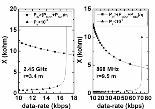
Our investigation will show that, for a passive RFID system compliant to European regulations in the 2.45 GHz or 868 MHz ISM frequency bands, the achievable operating range, considering a power consumption of the digital section of the transponder of 1 μW, is larger than 3.4 m and 9.5 m, respectively. At the same time, we will show that, for a passive 2.45-GHz RFID system, given an operating range of 3.4 meters, the achievable data-rate is about 17 kbps and for a passive 868-MHz RFID system, given an operating range of 9.5 meters, the achievable data-rate is about 70 kbps. Considering the more permissive US regulations, the maximum achievable operating distances are 11 m in the 2.45 GHz frequency band, and 29 m at 916 MHz, considering a data-rate of some tens of kbps. The extremely low power consumption considered for the digital logic is achievable by using subthreshold logic schemes, given that a simple finite state
Fig. 2-2: N-stage voltage multiplier and cascaded series voltage regulator. machine operating at a frequency smaller than 1 MHz is typically adequate to implement RFID protocols. However, such aspect is beyond the scope of the present paper and will not be discussed here.
2.2. Voltage Multiplier and Power Matching
Network
In this section we will describe the design criteria for both the voltage multiplier and the power matching network, in order to maximize the power efficiency of the transponder, defined as the ratio between the RF power available at the transponder’s antenna and the DC power at the output of the voltage multiplier available for supplying the transponder. As we will explain in the next section, the power efficiency of the transponder strongly affects the operating range of the tag-reader system.
2.2.1. N-stage Voltage Multiplier
An N-stage voltage multiplier consists of a cascade of N peak to peak detectors, as shown in Fig. 2-2 [2]. Let us suppose to apply, at the input of the voltage multiplier, a sinusoidal voltage, VIN, with a frequency f0 and an amplitude V0. In
order to ensure a small ripple in the output voltage VU, the capacitors indicated with C in Fig. 2-2 have to be dimensioned so that their time constant is much larger than
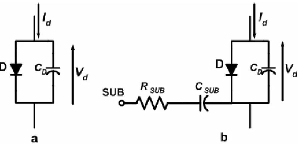
Fig. 2-3: Simplified equivalent circuit of the considered diodes: a) substrate losses neglected; b) equivalent circuit including substrate losses.
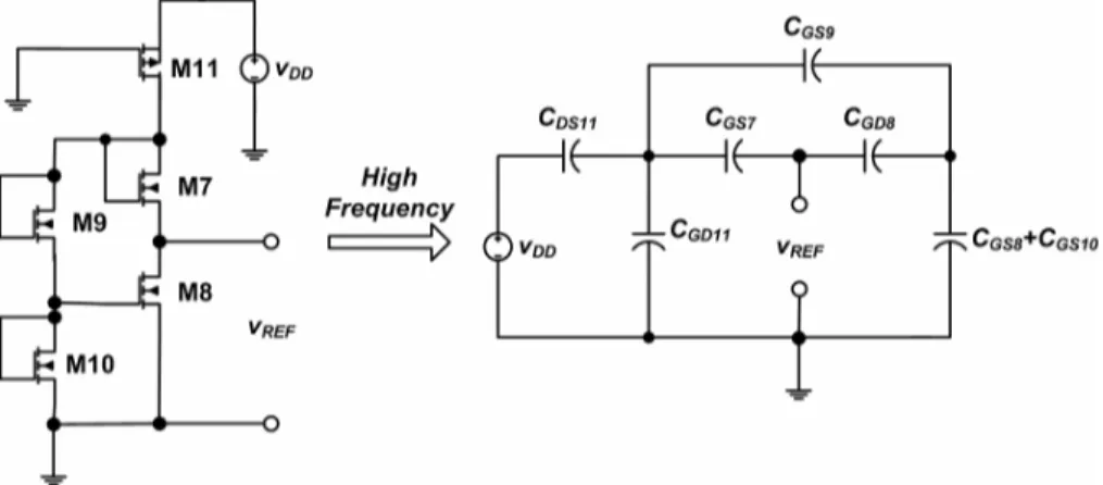
current. In this way, the voltage across C capacitors and the output voltage can be considered a DC voltage. As a consequence, in the high frequency analysis, it is possible to consider C capacitors as short-circuits and therefore all diodes appear to lie directly in parallel or anti-parallel to the input. In this situation the input RF voltage entirely drops across the diodes. In the DC analysis, C capacitors can be considered as open circuits, so that we have 2N identical diodes in series with the output. The voltage Vd that drops across each diode is therefore given by
N V t V V U d 2 ) cos( 0 0 − ± = ω , ( 2-1 ) where the sign ‘+’ is applied to diodes with even subscript (see Fig. 2-2) and the sign ‘-’ is applied to diodes with odd subscript. We can represent the equivalent circuit of the diode as an ideal diode in parallel with a capacitance, CD, as shown in
Fig. 2-3a, neglecting diode series resistances. Indeed, since the DC power required by RFID passive transponders is quite low (in the order of few μW), the DC output current of the voltage multiplier is very small leading to a negligible effect of the series resistance of the diodes. Such hypothesis was verified by circuit simulations. Thus the current Id in each diode is
dt dV C NV V t V V I I d D T U T S d + ⎥ ⎥ ⎦ ⎤ ⎢ ⎢ ⎣ ⎡ − ⎟⎟ ⎠ ⎞ ⎜⎜ ⎝ ⎛ − ⎟⎟ ⎠ ⎞ ⎜⎜ ⎝ ⎛ ± = 1 2 exp ) cos( exp 0 ω0 , ( 2-2 )
where IS is the diode saturation current and VT is the thermal voltage. We can