Università degli Studi di Ferrara
DOTTORATO DI RICERCA IN
"INGEGNERIA ELETTRONICA"
CICLO XXI
COORDINATORE Prof. Bertozzi Davide
Driving the Network-on-Chip Revolution
to Remove the Interconnect Bottleneck
in Nanoscale Multi-Processor Systems-on-Chip.
Settore Scientifico Disciplinare ING-INF/01
Dottorando Tutore
Dott. Medardoni Simone Prof. Bertozzi Davide
_______________________________ _____________________________
(firma) (firma)
ABSTRACT
The sustained demand for faster, more powerful chips has been met by the availability of chip manufacturing processes allowing for the integration of in-creasing numbers of computation units onto a single die. The resulting outcome, especially in the embedded domain, has often been called SYSTEM-ON-CHIP (SoC) or MULTI-PROCESSOR SYSTEM-ON-CHIP (MP-SoC).
MPSoC design brings to the foreground a large number of challenges, one of the most prominent of which is the design of the chip interconnection. With a number of on-chip blocks presently ranging in the tens, and quickly approaching the hundreds, the novel issue of how to best provide on-chip communication resources is clearly felt.
NETWORKS-ON-CHIPS (NoCs) are the most comprehensive and scalable answer to this design concern. By bringing large-scale networking concepts to the on-chip domain, they guarantee a structured answer to present and future communication requirements. The point-to-point connection and packet switch-ing paradigms they involve are also of great help in minimizswitch-ing wirswitch-ing overhead and physical routing issues. However, as with any technology of recent incep-tion, NoC design is still an evolving discipline. Several main areas of interest require deep investigation for NoCs to become viable solutions:
• The design of the NoC architecture needs to strike the best tradeoff among performance, features and the tight area and power constraints of the on-chip domain.
• Simulation and verification infrastructure must be put in place to explore, validate and optimize the NoC performance.
• NoCs offer a huge design space, thanks to their extreme customizability in terms of topology and architectural parameters. Design tools are needed to prune this space and pick the best solutions.
• Even more so given their global, distributed nature, it is essential to eval-uate the physical implementation of NoCs to evaleval-uate their suitability for next-generation designs and their area and power costs.
This dissertation performs a design space exploration of network-on-chip ar-chitectures, in order to point-out the trade-offs associated with the design of each individual network building blocks and with the design of network topol-ogy overall. The design space exploration is preceded by a comparative analysis of state-of-the-art interconnect fabrics with themselves and with early network-on-chip prototypes. The ultimate objective is to point out the key advantages that NoC realizations provide with respect to state-of-the-art communication infrastructures and to point out the challenges that lie ahead in order to make this new interconnect technology come true. Among these latter, technology-related challenges are emerging that call for dedicated design techniques at all levels of the design hierarchy. In particular, leakage power dissipation, contain-ment of process variations and of their effects. The achievecontain-ment of the above objectives was enabled by means of a NoC simulation environment for cycle-accurate modelling and simulation and by means of a back-end facility for the study of NoC physical implementation effects. Overall, all the results provided by this work have been validated on actual silicon layout.
Contents
1 Introduction 1
2 State of the Art SoC Communication Architecture 5
2.1 Introduction . . . 5
2.2 AMBA Bus . . . 6
2.2.1 AMBA System Bus . . . 7
2.2.2 AMBA AHB Basic Operation . . . 8
2.2.3 Advanced Peripheral Bus (APB) . . . 8
2.2.4 Advanced AMBA Evolutions . . . 9
2.3 CoreConnect Bus . . . 12
2.3.1 Processor Local Bus (PLB) . . . 13
2.3.2 On-Chip Peripheral Bus (OPB) . . . 14
2.3.3 Device Control Register Bus (DCR) . . . 15
2.4 STBus . . . 15
2.4.1 Bus topologies . . . 17
2.5 WishBone . . . 17
2.5.1 The Wishbone Bus Transactions . . . 18
2.6 SiliconBackplane MicroNetwork . . . 18
2.6.1 System Interconnect Bandwidth . . . 20
2.6.2 Configuration Resources . . . 20
2.7 Other On-Chip Interconnects . . . 20
2.7.1 Peripheral Interconnect Bus (PI-Bus) . . . 20
2.7.2 AVALON . . . 21
2.7.3 CoreFrame . . . 22
2.8 Conclusions . . . 23
3 Analysing the communication in a memory-centric industrial MPSoC platforms 27 3.1 Introduction . . . 27
3.2 MPSIM, a SystemC Platform Simulation . . . 28
3.3 MPSoC platform modelling . . . 30
3.3.1 STBus platform component models . . . 32
3.3.2 Architectural variants . . . 34
3.4 Interaction between communication and memory sub-systems . . 36
3.4.1 Single-layer architecture . . . 36
3.4.2 Multi-layer architecture . . . 37
3.5 Fine-grain platform performance analysis . . . 40
CONTENTS
3.7 Conclusion . . . 42
4 Network-on-Chip: An Interconnect Fabric For MPSoCs 49 4.1 Introduction . . . 49
4.2 Design Challenges For On-Chip Communication Architectures . . 51
4.2.1 Technology challenges . . . 51
4.2.2 Scalability challenges . . . 53
4.2.3 Design productivity challenges . . . 55
4.3 Network-On-Chip Architecture . . . 56 4.4 Network Interface . . . 56 4.5 Switch Architecture . . . 60 4.5.1 Æthereal . . . 62 4.5.2 Xpipes Lite . . . 63 4.6 Link Design . . . 64 4.6.1 Stall/Go . . . 65 4.6.2 T-Error . . . 65 4.6.3 Ack/Nack . . . 66
4.7 NoC design challenges . . . 67
4.8 Conclusion . . . 68
5 Switches: Architecture, Analysys and Optimization 73 5.1 Introduction . . . 73
5.2 Modelling and synthesis flow . . . 74
5.3 Basic switching fabric . . . 75
5.4 Control and datapath decoupling . . . 76
5.5 Spanning the area-latency-power trade-off . . . 78
5.5.1 Selection of switch architectures . . . 78
5.5.2 Area comparative analysis . . . 79
5.5.3 Performance comparative analysis . . . 79
5.5.4 Power/energy comparative analysis . . . 82
5.6 Conclusions . . . 84
6 Network Interface: Architecture, Analysys and Optimization 87 6.1 Design requirements . . . 88
6.2 NI sharing architectures . . . 90
6.2.1 Network interface architecture . . . 90
6.2.2 Merger architecture . . . 91
6.3 Optimizations . . . 92
6.4 Synthesis results . . . 93
6.5 Basic performance tests . . . 94
6.6 System-level analysis . . . 96
6.6.1 Application-specific topology . . . 96
6.6.2 General purpose topology . . . 98
6.7 Conclusions . . . 100
7 Designing Regular Network-on-Chip Topologies under Technol-ogy and Architecture Constraints 105 7.1 Backend synthesis flow . . . 107
7.2 Topology exploration . . . 108
CONTENTS
7.2.2 Topologies under test: k-ary n-meshes . . . 109
7.2.3 Topologies under test: k-ary n-Tree . . . 111
7.3 Physical design: k-ary n-meshes . . . 114
7.3.1 16 tile networks . . . 114
7.3.2 64 tile networks . . . 115
7.4 Physical design: k-ary n-Tree . . . 116
7.5 Post-Layout analysis: k-ary n-mesh . . . 119
7.5.1 16 tile . . . 119
7.5.2 64 tile . . . 120
7.6 Post-Layout analysis: k-ary n-Tree . . . 121
7.7 Conclusions . . . 124 7.7.1 k-ary n-meshes . . . 125 7.7.2 k-ary n-Tree . . . 125 8 Emerging Issue 133 8.1 Introduction . . . 133 8.2 Architectural Implications . . . 134
8.2.1 Routing Mechanisms and Algorithms . . . 135
8.2.2 Modelling within-die variability . . . 138
8.2.3 Evaluation . . . 140 8.3 Circuit Implications . . . 148 8.3.1 Self-correcting flip-flop . . . 149 8.3.2 Link Design . . . 151 8.3.3 Experimental results . . . 155 8.4 Conclusions . . . 157
9 Power-Optimal RTL Soft-Macro Selection Strategy for Leakage-Sensitive Technologies 163 9.1 Introduction . . . 163
9.2 Synthesis methodology . . . 165
9.2.1 Performance-optimized synthesis flow . . . 165
9.2.2 Power-optimized synthesis flow . . . 165
9.2.3 Multi-Vth synthesis flow . . . 167
9.3 Experimental results . . . 167
9.3.1 Energy characterization of adder units . . . 167
9.3.2 The impact of power optimizations . . . 171
9.3.3 The impact of multi-Vth design . . . 172
9.4 Comparison with default DW selection strategy . . . 175
9.5 Conclusions . . . 176
10 Conclusion and Future work 183 10.1 Conclusions . . . 183 10.2 Future Work . . . 184 10.3 Scientific Publication . . . 184 10.3.1 Proceedings . . . 185 10.3.2 Magazine . . . 188 10.3.3 Poster . . . 189 10.3.4 Patent . . . 189
Chapter 1
Introduction
Silicon vendors are constantly facing pressure to deliver feature-rich, high-performance, low-power, low-cost chips, in as short a time as possible. Luckily, silicon manufacturing techniques have been continuously perfected, following the well-known Moore’s Law; this has provided the potential for answering cus-tomer demands.
However, along the years, an increasing gap has been observed among the number of available on-chip transistors and the capability of designers to make good use of them. As a consequence, some trends in chip design have become crystal clear:
• An increasing emphasis on modularity, reuse and parallelism is mandatory. Redesign from scratch is too time-consuming. Also, deploying multiple instances of existing computation blocks can be more efficient than devel-oping more powerful blocks. Therefore, libraries of so-called INTELLEC-TUAL PROPERTY (IP) cores are increasingly becoming the foundation of platform development.
• Also based on the previous item, complexity is nowadays shifting from the development of functional units to the task of system integration. This is exacerbated by the fact that full designs are nowadays almost impossible to characterize in all possible operating conditions, leading to closure, optimization and verification issues.
• Software tools devoted to design automation are key at all levels. This ap-plies to performance characterization, platform assembly and validation, physical implementation, etc.. Without efficient tools, the sheer complex-ity of billion-transistor designs and deep-submicron lithographic processes is impossible to tackle by designer teams of any size.
A typical outcome of these trends are today’s MULTI-PROCESSOR-SYSTEMS-ON-CHIPS (MPSoCs). These are full-featured chips, composed of a variety of functional blocks, to the point of integrating the foundation of a whole system or device into a single die. MPSoCs are used in a variety of envi-ronments, including multimedia gadgets, gaming stations, smartphones, auto-motive equipment, healthcare devices, industrial machinery, aerospace control units, and many more. MPSoCs are built upon assemblies of IP cores, and
CHAPTER 1. INTRODUCTION
rely extensively on COMPUTER AIDED DESIGN (CAD) tooling for initial design space exploration, system optimization, system verification, and physical implementation.
An increasingly critical piece of the MPSoC puzzle is the on-chip intercon-nection infrastructure. Today, even MPSoCs used in mid-range mobile phones can easily contain tens of IP cores, and new chips with more than a hundred such internal units are appearing for various applications. The trend expressing the number of IP cores that can be integrated on a chip is exponential, roughly doubling every 18 months. How to effectively provide communication resources among such a number of building blocks is clearly a challenge. In fact, it is likely a key factor in determining the success or failure of upcoming MPSoCs will be the ability to efficiently provide the communication backbone into which to seamlessly plug a variety of IP cores.
A comprehensive solution to on-chip interconnection issues has been pro-posed in the form of NETWORKS-ON-CHIPS (NoCs).
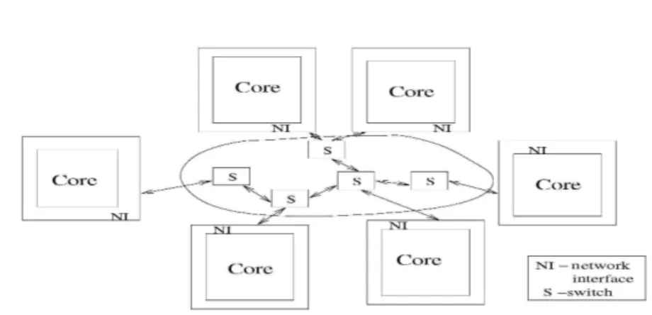
NoCs are packet-switching networks, brought to the on-chip level. The ra-tionale is that, since the complexity of on-chip communication is rapidly ap-proaching that of large area systems in terms of actors, it makes sense to reuse some of the solutions devised in the latter space. Therefore, NoCs are based upon topologies of switches (also called routers) distributing packets around, over point-to-point links. Since existing IP cores do not normally communicate by means of packets, NETWORK INTERFACES (NIs ) (also called network adapters) are in charge of protocol conversion; they convert commands appear-ing on the pinout of IP cores into packets, and vice versa at the receivappear-ing end of a transaction. NoCs have the potential to bring a large number of advantages to on-chip communication, such as:
• Virtually unlimited architectural scalability. As known from wide area networks, it is easy to comply with higher bandwidth requirements by larger numbers of cores simply by deploying more switches and links. • Much better electrical performance. All connections are point-to-point.
The length of inter-switch links is a design parameter that can be ad-justed. The wire parallelism in links can be controlled at will, since packet transmission can be serialized. All these factors imply faster propagation times and total control over crosstalk issues.
• Also due to the possibility of having narrower links than in buses (e.g. 32 bits instead of 100), routing concerns are greatly alleviated, and wiring overhead is dramatically reduced. This leads to higher wire utilization and efficiency.
• Faster and easier design closure achievement. Physical design improve-ments make NoCs, in general, more predictable than buses. Therefore, it is more unlikely that costly respins will be required upon physical design and performance qualification.
• Better performance under load. Since the operating frequency can be higher than in buses, the data width is a parameter, and communica-tion flows can be handled in parallel with suitable NoC topology design, virtually any bandwidth load can be tackled.
• More modular, plug&play-oriented approach to system assembly. IP cores are attached in point-to-point fashion to dedicated NIs; NIs can be spe-cialized for any interface that may be needed, either industry standards such as AMBA AHB or any custom protocol. Potentially any core may be seamlessly attached to a NoC given the proper NI. Computation and communication concerns are clearly decoupled at the NI level.
• Potential for the development of streamlined design flows. While hierar-chical buses are often assembled by hand and therefore must be tuned and validated with manual intervention, a network can be designed, optimized and verified by automated means, leading to large savings in design times, and getting a solution closer to optimality.
• A much larger design space. NoCs can be tuned in a variety of parameters (topology, buffering, data widths, arbitrations, routing choices, etc.), lead-ing to higher chances of optimally matchlead-ing design requirements. Belead-ing distibuted, modular structures, NoCs can also accommodate differently tuned regions. For example, some portions of a NoC could be tuned stat-ically for lower resource usage and lower performance (e.g. by reducing the data width), or could dynamically adjust their mode of operation (e.g. frequency, voltage scaling).
At the same time, NoCs are facing a completely different set of constraints compared to wide area networks. While in the latter environment a switch is implemented with at least one dedicated chip, in a NoC the switch must occupy a tiny fraction of the chip real estate. This means that some of the principles acquired in wide area networking have to be revisited. Some of the challenges lying ahead of NoCs include:
• The tradeoffs among network features, area and power budgets have to be studied from scratch. Policies which are widely accepted in general networking (e.g. dynamic packet routing) must be reassessed to evaluate their impact on silicon area.
• Performance requirements are very different in the on-chip domain, also due to the completely different properties of on-chip wiring. Bandwidth milestones are much easier to achieve, since information transfer across on-chip wires is much faster than across long cables. Conversely, latency bounds are much stricter; while milliseconds or even hundreds of millisec-onds are acceptable for wide area networks, IP cores on a chip normally require response times of few nanoseconds.
• Contrary to wide area networks, where nodes may often be dynamically connected to and disconnected from the network, in NoCs the set of at-tached IP cores is obviously fixed. In many applications, it is also rela-tively easy to statically characterize the traffic profiles of such IP cores. This opens up the possibility of thoroughly customizing NoCs for specific workloads. How to achieve this goal is, however, less clear.
• Design tools for NoCs can be developed, but, as above, how exactly is an open question. The customizability of NoCs, while an asset, is also an issue when it comes to devising tools capable of pruning the design space
CHAPTER 1. INTRODUCTION
in search of the optimal solutions. The problem is compounded by the need to take into account both architectural and physical properties; by the need to guarantee design closure; and by the need to validate that the outcome is fully functional, e.g. deadlock-free and compliant with performance objectives.
• NoCs are a recent technology, and as such, they are in need of the de-velopment of thorough infrastructure. In addition to design tools, this includes simulators, emulation platforms, and back-end flows for the im-plementation on APPLICATION-SPECIFIC INTEGRATED CIRCUITS (ASICS).
The main objective of this dissertation is to perform a design space explo-ration of network-on-chip architectures, in order to point-out the trade-offs as-sociated with the design of each individual network building block and with the design of network topology overall. This exploration aims at providing guide-lines to system designers as to the most suitable network design configuration to meet predefined performance, area and power constraints. The design space ex-ploration is preceded by a comparative analysis of state-of-the-art interconnect fabrics with themselves and with early network-on-chip prototypes. The ulti-mate objective is to point out the key advantages that NoC realizations provide with respect to state-of-the-art communication infrastructures and to point out the challenges that lie ahead in order to make this new interconnect technol-ogy come true. Among these latter, technoltechnol-ogy-related challenges are emerging that call for dedicated design techniques at all levels of the design hierarchy. In particular, leakage power dissipation, containment of process variations and of their effects. The achievement of the above objectives was enabled by means of a NoC simulation environment for cycle-accurate modelling and simulation and by means of a back-end facility for the study of NoC physical implementation effects. Overall, all the results provided by this work have been validated on actual silicon layout.
Chapter 2
State of the Art SoC
Communication
Architecture
2.1
Introduction
The current high levels of on-chip integration allow for the implementation of increasingly complex Systems-on-Chip (SoCs), consisting of heterogeneous com-ponents such as general purpose processors, DSPs, coprocessors, memories, I/O units, and dedicated hardware accelerators.
In this context, Multi-Processor Systems-on-Chip (MPSoCs) are emerging as an effective solution to meet the demand for computational power posed by application domains such as network processors and parallel media processors. MPSoCs combine the advantages of parallel processing with the high integration levels of Systems-on-Chips (SoCs).
It is expected that future MPSoCs will integrate hundreds of processing units and storage elements, and their performance will be increasingly interconnect-dominated [21]. Interconnect technology and architecture will become the limit-ing factor for achievlimit-ing operational goals, and the efficient design of low-power, high-performance on-chip communication architectures will pose novel chal-lenges. The main issue regards scalability of system interconnects, since the trend for system integration is expected to continue. State-of-the-art on-chip buses rely on shared communication resources and on an arbitration mechanism which is in charge of serializing bus access requests. This widely adopted solu-tion unfortunately suffers from power and performance scalability limitasolu-tions, therefore a lot of effort is being devoted to the development of advanced bus topologies (e.g., partial or full crossbars, bridged buses) and protocols, some of them already implemented in commercially available products. In the long run, a more aggressive approach will be needed, and a design paradigm shift will most probably lead to a packetized on-chip communication based on micronetworks of interconnects or Networks-on-Chip (NoCs) [17, 15].
This chapter focuses on state-of-the-art SoC communication architectures, providing an overview of the most relevant ones from an industrial and research
CHAPTER 2. STATE OF THE ART SOC COMMUNICATION ARCHITECTURE 0000 0000 0000 0000 0000 0000 0000 0000 0000 1111 1111 1111 1111 1111 1111 1111 1111 1111 SDRAM controller Colour Controller LCD ARM CPU Smart Card I/F UART Serial Port Synchronous AMBA−(AHB) System bus AMBA−(APB) Peripheral bus
high speed low power
external memory Bridge Audio Codec I/F Test I/F Controller SRAM
Figure 2.1: Schematic architecture of AMBA bus.
viewpoint. Open bus specifications such as AMBA and CoreConnect will be obviously described more in detail, providing the background which is needed to understand the necessarily more general description of proprietary industrial bus architectures, while at the same time being able to assess their contribution to the advance in the field.
2.2
AMBA Bus
AMBA (Advanced Micro-Controller Bus Architecture) is a bus standard which was originally conceived by ARM to support communication among ARM pro-cessor cores. However, nowadays AMBA is one of the leading on-chip busing systems because it is licensed and deployed for use with third party IP cores [1]. Designed for custom silicon, the AMBA specification provides standard bus protocols for connecting on-chip components, custom logic and specialized func-tions. These bus protocols are independent of the ARM processor and general-ized for different SoC structures.
AMBA defines a segmented bus architecture, wherein two bus segments are connected with each other via a bridge that buffers data and operations between them. A system bus is defined, which provides a high-speed, high-bandwidth communication channel between embedded processors and high-performance peripherals. Two system buses are actually specified: the AMBA High-Speed
Bus (AHB) and the Advanced System Bus (ASB).
Moreover, a low-performance and low power peripheral bus (called Advanced
Peripheral Bus, APB) is specified, which accommodates communication with
general purpose peripherals and is connected to the system bus via a bridge, acting as the only APB master. The overall AMBA architecture is illustrated in figure 2.1.
2.2. AMBA BUS
2.2.1
AMBA System Bus
ASB is the first generation of AMBA system bus, and sits above APB in that it implements the features required for high-performance systems including burst transfers, pipelined transfer operation and multiple bus masters. AHB is a later generation of AMBA bus which is intended to address the requirements of high-performance, high-clock synthesizable designs. ASB is used for simpler, more cost-effective designs whereas more sophisticated designs call for the employ-ment of the AHB. For this reason, a detailed description of AHB follows.
The main features of AMBA AHB can be summarized as follows:
• Multiple bus masters. Optimized system performance is obtained by shar-ing resources among different bus masters. A simple request-grant mech-anism is implemented between the arbiter and each bus master. In this way, the arbiter ensures that only one bus master is active on the bus and also that when no masters are requesting the bus a default master is granted.
• Pipelined and burst transfers. Address and data phases of a transfer occur during different clock periods. In fact, the address phase of any transfer occurs during the data phase of the previous transfer. This overlapping of address and data is fundamental to the pipelined nature of the bus and allows for high performance operation, while still providing adequate time for a slave to provide the response to a transfer. This also implies that ownership of the data bus is delayed with respect to ownership of the address bus. Moreover, support for burst transfers allows for efficient use of memory interfaces by providing transfer information in advance. • Split transactions. They maximize the use of bus bandwidth by enabling
high latency slaves to release the system bus during dead time while they complete processing of their access requests.
• Wide data bus configurations. Support for high-bandwidth data-intensive applications is provided using wide on-chip memories. System buses sup-port 32, 64, and 128-bit data-bus implementations with a 32-bit address bus, as well as smaller byte and half-word designs.
• Non-tristate implementation. AMBA AHB implements a separate read and write data bus in order to avoid the use of tristate drivers. In partic-ular, master and slave signals are multiplexed onto the shared communi-cation resources (read and write data buses, address bus, control signals). A typical AMBA AHB system contains the following components:
AHB master: Only one bus master at a time is allowed to initiate and com-plete read and write transactions. Bus masters drive out the address and control signals and the arbiter determines which master has its signals routed to all of the slaves. A central decoder controls the read data and response signal multiplexor, which selects the appropriate signals from the slave that has been addressed.
AHB slave: It signals back to the active master the status of the pending transaction. It can indicate that the transfer completed successfully, or
CHAPTER 2. STATE OF THE ART SOC COMMUNICATION ARCHITECTURE
that there was an error or that the master should retry the transfer or indicate the beginning of a split transaction.
AHB arbiter: The bus arbiter serializes bus access requests. The arbitration algorithm is not specified by the standard and its selection is left as a de-sign parameter (fixed priority, round-robin, latency-driven, etc.), although the request-grant based arbitration protocol has to be kept fixed.
AHB decoder: This is used for address decoding and provides the select signal to the intended slave.
2.2.2
AMBA AHB Basic Operation
In a normal bus transaction, the arbiter grants the bus to the master until the transfer completes and the bus can then be handed over to another master. However, in order to avoid excessive arbitration latencies, the arbiter can break up a burst. In that case, the master must re-arbitrate for the bus in order to complete the remaining data transfers.
A basic AHB transfer consists of four clock cycles. During the first one, the request signal is asserted, and in the best case at the end of the second cycle a grant signal from the arbiter can be sampled by the master. Then, address and control signals are asserted for slave sampling on the next rising edge, and during the last cycle the data phase is carried out (read data bus driven or information on the write data bus sampled). A slave may insert wait states into any transfer, thus extending the data phase, and a ready signal is available for this purpose.
Four, eight and sixteen-beat bursts are defined in the AMBA AHB protocol, as well as undefined-length bursts. During a burst transfer, the arbiter rear-bitrates the bus when the penultimate address has been sampled, so that the asserted grant signal can be sampled by the relative master at the same point where the last address of the burst is sampled. This makes bus master handover at the end of a burst transfer very efficient.
For long transactions, the slave can decide to split the operation warning the arbiter that the master should not be granted access to the bus until the slave indicates it is ready to complete the transfer. This transfer splitting mechanism is supported by all advanced on-chip interconnects, since it prevents high latency slaves from keeping the bus busy without performing any actual transfer of data. On the contrary, split transfers can significantly improve bus efficiency, i.e. reduce the number of bus busy cycles used just for control (e.g. protocol handshake) and not for actual data transfers. Advanced arbitration features are required in order to support split transfers, as well as more complex master and slave interfaces.
2.2.3
Advanced Peripheral Bus (APB)
The AMBA APB is intended for general-purpose low-speed low-power periph-eral devices. It enables the connection to the main system bus via a bridge. All bus devices are slaves, the bridge being the only peripheral bus master.
This is a static bus that provides a simple addressing, with latched addresses and control signals for easy interfacing. ARM recommends a dual Read and
2.2. AMBA BUS
Write bus implementation, but APB can be implemented with a single tristated data bus.
The main features of this bus are the following: • Unpipelined architecture.
• Low gate count. • Low power operation.
– Reduced loading of the main system bus is obtained by isolating the peripherals behind the bridge.
– Peripheral bus signals are only active during low-bandwidth periph-eral transfers.
AMBA APB operation can be abstracted as a state machine with three states. The default state for the peripheral bus is IDLE, which switches to
SETUP state when a transfer is required. SETUP state lasts just one cycle,
during which the peripheral select signal is asserted. The bus then moves to
ENABLE state, which also lasts only one cycle and which requires the address,
control and data signals to remain stable. Then, if other transfers are to take place, the bus goes back to SETUP state, otherwise to IDLE. As can be ob-served, AMBA APB should be used to interface to any peripherals which are low-bandwidth and do not require the high performance of a pipelined bus in-terface.
2.2.4
Advanced AMBA Evolutions
Recently, some advanced specifications of AMBA bus have appeared, featuring increased performance and better link utilization. In particular, the Multi-Layer
AHB and the AMBA AXI interconnect schemes will be briefly addressed in the
following sub-sections.
It should be observed that interconnect performance improvement can be achieved by adopting new topologies and by choosing new protocols, at the expense of silicon area. The former strategy leads from shared buses to bridged clusters, partial or full crossbars, and eventually to Networks-on-Chip (NoCs), in an attempt to increase available bandwidth and to reduce local contention. The latter strategy instead tries to maximize link utilization by adopting more sophisticated control schemes and thus permitting a better sharing of existing resources.
Multi-Layer AHB can be seen as an evolution of bus topology while keeping the AHB protocol unchanged. On the contrary, AMBA AXI represents an advanced interconnect fabric protocol.
Multi-layer AHB
The Multi-Layer AHB specification emerges with the aim of increasing the over-all bus bandwidth and providing a more flexible interconnect architecture with respect to AMBA AHB. This is achieved by using a more complex interconnec-tion matrix which enables parallel access paths between multiple masters and slaves in a system [2].
CHAPTER 2. STATE OF THE ART SOC COMMUNICATION ARCHITECTURE Master Master Slave Slave Slave Slave Interconnect matrix
Figure 2.2: Schematic view of the multi-layer AHB interconnect
Therefore, the multi-layer bus architecture allows the interconnection of un-modified standard AHB master and slave modules with an increased available bus bandwidth. The resulting architecture becomes very simple and flexible: each AHB layer only has one master and no arbitration and master-to-slave muxing is needed. Moreover, the interconnect protocol implemented in these layers can be very simple: it does not have to support request and grant, nor retry or split transactions.
The additional hardware needed for this architecture with respect to the AHB is a multiplexor to connect the multiple masters to the peripherals and some point arbitration is also required when more than one master wants to access the same slave simultaneously.
Figure 2.2 shows a schematic view of the multi-layer concept. The inter-connect matrix contains a decode stage for every layer in order to determine which slave is required during the transfer. The multiplexer is used to route the request from the specific layer to the desired slave.
The arbitration protocol decides the sequence of accesses of layers to slaves based on a priority assignment. The layer with lowest priority has to wait for the slave to be freed. Different arbitration schemes can be used, and every slave port has its own arbitration. Input layers can be served in a round-robin fashion, changing every transfer or every burst transaction, or based on a fixed priority scheme.
The number of input/output ports on the interconnect matrix is completely flexible and can be adapted to suit to system requirements. As the number of masters and slaves implemented in the system increases, the complexity of the interconnection matrix can become significant and some optimization techniques have to be used: defining multiple masters on a single layer, multiple slaves appearing as a single slave to the interconnect matrix, defining local slaves to a particular layer.
2.2. AMBA BUS Read data Read data Read data Address and control
Read address channel
Read data channel Master Interface Slave Interface Address and control Write response data data
Write Write Write data Write address channel
Write data channel
Write response channel Master
Interface
Slave
Interface
a) b)
Figure 2.3: Architecture of transfers: a) Read operation; b) Write operation.
Finally, it is interesting to outline the capability of this topology to support multi-port slaves. Some devices, such as SDRAM controllers, work much more efficiently when processing transfers from different layers in parallel.
AMBA AXI Protocol
AXI is the latest generation AMBA interface. It is designed to be used as a high-speed submicron interconnect, and also includes optional extensions for low-power operation [3]. This high-performance protocol provides flexibility in the implementation of interconnect architectures while still keeping backward-compatibility with existing AHB and APB interfaces.
AMBA AXI builds upon the concept of point-to-point connection. AMBA AXI does not provide masters and slaves with visibility of the underlying inter-connect, instead featuring the concept of master interfaces and symmetric slave
interfaces. This approach, besides allowing seamless topology scaling, has the
advantage of simplifying the handshake logic of attached devices, which only need to manage a point-to-point link.
To provide high scalability and parallelism, four different logical monodi-rectional channels are provided in AXI interfaces: an address channel, a read channel, a write channel and a write response channel. Activity on different channels is mostly asynchronous (e.g. data for a write can be pushed to the write channel before or after the write address is issued to the address channel), and can be parallelized, allowing multiple outstanding read and write requests. Figure 2.3a shows how a read transaction uses the read address and read data channels. The write operation over the write address and write data channels is presented in Figure 2.3b.
As can be observed, the data is transferred from the master to the slave using a write data channel, and it is transferred from the slave to the master using a read data channel. In write transactions, in which all the data flows from the master to the slave, the AXI protocol has an additional write response channel to allow the slave to signal to the master the completion of the write transaction.
However, the AXI protocol is a master/slave-to-interconnect interface def-inition, and this enables a variety of different interconnect implementations.
CHAPTER 2. STATE OF THE ART SOC COMMUNICATION ARCHITECTURE
Therefore, the mapping of channels, as visible by the interfaces, to actual inter-nal communication lanes is decided by the interconnect designer; single resources might be shared by all channels of a certain type in the system, or a variable amount of dedicated signals might be available, up to a full crossbar scheme. The rationale of this split-channel implementation is based upon the observa-tion that usually the required bandwidth for addresses is much lower than that for data (e.g. a burst requires a single address but maybe four or eight data transfers). Availability of independently scalable resources might, for example, lead to medium complexity designs sharing a single internal address channel while providing multiple data read and write channels.
Finally, some of the key incremental features of the AXI protocol can be listed as follows:
• support for out-of-order completion of transactions • easy addition of register stages to provide timing closure • support for multiple address issuing
• separate read and write data channels to enable low-cost Direct Memory Access (DMA)
• support for unaligned data transfers
2.3
CoreConnect Bus
CoreConnect is an IBM-developed on-chip bus that eases the integration and reuse of processor, sub-system and peripheral cores within standard product platform designs. It is a complete and versatile architecture clearly targeting high performance systems, and many of its features might be overkill in simple embedded applications [13].
The CoreConnect bus architecture serves as the foundation of IBM Blue LogicTMor other non-IBM devices. The Blue Logic ASIC/SOC design
method-ology is the approach proposed by IBM [6] to extend conventional ASIC design flows to current design needs: low-power and multiple-voltage products, re-configurable logic, custom design capability, and analog/mixed-signal designs. Each of these offerings requires a well-balanced coupling of technology capa-bilities and design methodology. The use of this bus architecture allows the hierarchical design of SoCs.
As can be seen in figure 2.4, the IBM CoreConnect architecture provides three buses for interconnecting cores, library macros, and custom logic:
• Processor Local Bus (PLB). • On-Chip Peripheral Bus (OPB). • Device Control Register (DCR) Bus.
The PLB bus connects the processor to high-performance peripherals, such as memories, DMA controllers, and fast devices. Bridged to the PLB, the OPB supports slower-speed peripherals. Finally, the DCR bus is a separate control bus that connects all devices, controllers, and bridges and provides a separate
2.3. CORECONNECT BUS Core System Core System Core System Arbiter Arbiter Bridge Bus (OPB) On−Chip Peripheral Bus (PLB)
Processor Local Bus
Core Core Peripheral Peripheral Core Memory On−Chip Processor Processor Auxiliary DCR Bus DCR Bus CoreConnect Bus
Figure 2.4: Schematic structure of the CoreConnect bus.
path to set and monitor the individual control registers. It is designed to transfer data between the CPU’s general purpose registers and the slave logic’s device control registers. It removes configuration registers from the memory address map, which reduces loading and improves bandwidth of the PLB.
This architecture shares many high-performance features with the AMBA Bus specification. Both architectures allow split, pipelined and burst transfers, multiple bus masters and 32, 64 or 128-bits architectures. On the other hand, CoreConnect also supports multiple masters in the peripheral bus.
Please note that design toolkits are available for the CoreConnect bus and include functional models, monitors, and a bus functional language to drive the models. These toolkits provide an advanced validation environment for engineers designing macros to attach to the PLB, OPB and DCR buses.
2.3.1
Processor Local Bus (PLB)
The PLB is the main system bus targeting high performance and low latency on-chip communication. More specifically, PLB is a synchronous, multi-master, arbitrated bus. It supports concurrent read and write transfers, thus yielding a maximum bus utilization of two data transfers per clock cycle. Moreover, PLB implements address pipelining, that reduces bus latency by overlapping a new write request with an ongoing write transfer and up to three read requests with an ongoing read transfer [14].
Access to PLB is granted through a central arbitration mechanism that allows masters to compete for bus ownership. This arbitration mechanism is flexible enough to provide for the implementation of various priority schemes. In fact, four levels of request priority for each master allow PLB implementation with various arbitration priority schemes. Additionally, an arbitration locking mechanism is provided to support master-driven atomic operations. PLB also exhibits the ability to overlap the bus request/grant protocol with an ongoing transfer.
The PLB specification describes a system architecture along with a detailed description of the signals and transactions. PLB-based custom logic systems require the use of a PLB macro to interconnect the various master and slave
CHAPTER 2. STATE OF THE ART SOC COMMUNICATION ARCHITECTURE
macros.
The PLB macro is the key component of PLB architecture, and consists of a bus arbitration control unit and the control logic required to manage the address and data flow through the PLB. Each PLB master is attached to the PLB through separate address, read data and write data buses and a plurality of transfer qualifier signals, while PLB slaves are attached through shared, but
decoupled, address, read data and write data buses (each one with its own
trans-fer control and status signals). The separate address and data buses from the masters allow simultaneous transfer requests. The PLB macro arbitrates among them and sends the address, data and control signals from the granted master to the slave bus. The slave response is then routed back to the appropriate master. Up to 16 masters can be supported by the arbitration unit, while there are no restrictions in the number of slave devices.
2.3.2
On-Chip Peripheral Bus (OPB)
Frequently, the OPB architecture connects low-bandwidth devices such as serial and parallel ports, UARTs, timers, etc. and represents a separate, independent level of bus hierarchy. It is implemented as a multi-master, arbitrated bus. It is a fully synchronous interconnect with a common clock, but its devices can run with slower clocks, as long as all of the clocks are synchronized with the rising edge of the main clock.
This bus uses a distributed multiplexer attachment implementation instead of tristate drivers. The OPB supports multiple masters and slaves by imple-menting the address and data buses as a distributed multiplexer. This type of structure is suitable for the less data intensive OPB bus and allows adding peripherals to a custom core logic design without changing the I/O on either the OPB arbiter or existing peripherals. All of the masters are capable of providing an address to the slaves, whereas both masters and slaves are capable of driving and receiving the distributed data bus.
PLB masters gain access to the peripherals on the OPB bus through the OPB bridge macro. The OPB bridge acts as a slave device on the PLB and a master on the OPB. It supports word (32-bit), half-word (16-bit) and byte read and write transfers on the 32-bit OPB data bus, bursts and has the capabil-ity to perform target word first line read accesses. The OPB bridge performs dynamic bus sizing, allowing devices with different data widths to efficiently communicate. When the OPB bridge master performs an operation wider than the selected OPB slave can support, the bridge splits the operation into two or more smaller transfers.
Some of the main features of the OPB specification are: • Fully synchronous
• Dynamic bus sizing: byte, halfword, fullword and doubleword transfers • Separate address and data buses
• Support for multiple OPB bus masters
• Single cycle transfer of data between OPB bus master and OPB slaves • Sequential address (burst) protocol
2.4. STBUS
• 16-cycle fixed bus timeout provided by the OPB arbiter • Bus arbitration overlapped with last cycle of bus transfers • Optional OPB DMA transfers
2.3.3
Device Control Register Bus (DCR)
The DCR bus provides an alternative path to the system for setting the indi-vidual device control registers. These latter are on-chip registers that are imple-mented outside the processor core, from an architectural viewpoint. Through the DCR bus, the host CPU can set up the device-control-register sets without loading down the main PLB. This bus has a single master, the CPU interface, which can read or write to the individual device control registers. The DCR bus architecture allows data transfers among OPB peripherals to occur inde-pendently from, and concurrently with data transfers between processor and memory, or among other PLB devices. The DCR bus architecture is based on a ring topology to connect the CPU interface to all devices. The DCR bus is typicallly implemented as a distributed multiplexer across the chip such that each sub-unit not only has a path to place its own DCRs on the CPU read path, but has also a path which bypasses its DCRs and places another unit’s DCRs on the CPU read path. DCR bus consists of a 10-bit address bus and a 32-bit data bus.
This is a synchronous bus, wherein slaves may be clocked either faster or slower than the master, although a synchronization of clock signals with the DCR bus clock is required.
Finally, bursts are not supported by this bus, and 2-cycle minimum read or write transfers are allowed. Optionally, they can be extended by slaves or by the single master.
2.4
STBus
STBus is an STMicroelectronics proprietary on-chip bus protocol. STBus is dedicated to SoC designed for high bandwidth applications such as audio/video processing [20]. The STBus interfaces and protocols are closely related to the industry standard VCI (Virtual Component Interface). The components inter-connected by an STBus are either initiators (which initiate transactions on the bus by sending requests), or targets (which respond to requests). The bus ar-chitecture is decomposed into nodes (sub-buses in which initiators and targets can communicate directly), and the internode communications are performed through FIFO buffers. Figure 2.5 shows a schematic view of the STBus inter-connect.
STBus implements three different protocols that can be selected by the de-signer in order to meet the complexity, cost and performance constraints. From lower to higher, they can be listed as follows:
Type 1: Peripheral Protocol. This type is the low cost implementation for low/medium performance. Its simple design allows a synchronous hand-shake protocol and provides a limited transaction set. The peripheral STBus is targeted at modules which require a low complexity medium
CHAPTER 2. STATE OF THE ART SOC COMMUNICATION ARCHITECTURE
Type 1 Type 2 Type 3
Type 1 Type 2 Type 3 Initiators (masters) Targets (slaves) Initiator IP any bus IF stbus IF stbus IF anybus IF initiator IP
STBus
Figure 2.5: Schematic view of the STBus interconnect
data rate communication path with the rest of the system. This typi-cally includes standalone modules such as general-purpose input/output or modules which require independent control interfaces in addition to their main memory interface.
Type 2: Basic Protocol. In this case, the limited operation set of the Pe-ripheral Interface is extended to a full operation set, including compound operations, source labeling and some priority and transaction labeling. Moreover, this implementation supports split and pipelined accesses, and is aimed at devices which need high performance but do not require the ad-ditional system efficiency associated with shaped request/response packets or the ability to re-order outstanding operations.
Type 3: Advanced Protocol. The most advanced implementation up-grades previous interfaces with support for out-of-order execution and shaped packets, and is equivalent to the Advanced VCI protocol. Split and pipelined accesses are supported. It allows performance improve-ments either by allowing more operations to occur concurrently, or by rescheduling operations more efficiently.
A type 2 protocol preserves the order of requests and responses. One con-straint is that, when communicating with a given target, an initiator cannot send a request to a new target until it has received all the responses from the current target. The unresponded requests are called pending, and a pending request controller manages them. A given type 2 target is assumed to send the responses in the same order as the request arrival order. In type 3 protocol, the order of responses may not be guaranteed, and an initiator can communicate with any target, even if it has not received all responses from a previous one.
Associated with these protocols, hardware components have been designed in order to build complete reconfigurable interconnections between Initiators and Targets. A toolkit has been developed around this STBus (graphical in-terface) to generate automatically top level backbone, cycle accurate high level
2.5. WISHBONE
models,way to implementation, bus analysis (latencies, bandwidth) and bus ver-ification (protocol and behavior).
An STBus system includes three generic architectural components. The node arbitrates and routes the requests and optionally, the responses. The converter is in charge of converting the requests from one protocol to another (for instance, from basic to advanced). Finally, the size converter is used between two buses of the same type but of different widths. It includes buffering capability.
The STBus can implement various strategies of arbitration and allows to change them dynamically. In a simplified single-node system example, a com-munication between one initiator and a target is performed in several steps.
• a request/grant step between the initiator and the node takes place, cor-responding to an atomic rendez-vous operation of the system;
• the request is transferred from the node to the target;
• a response-request/grant step is carried out between the target and the node;
• the response-request is transferred from the node to the initiator.
2.4.1
Bus topologies
STBus can instantiate different bus topologies, trading-off communication par-allelism with architectural complexity. In particular, system interconnects with different scalability properties can be instantiated such as:
• Single Shared Bus: suitable for simple low-performance implementations. It features minimum wiring area but limited scalability;
• Full Crossbar: targets complex high-performance implementations. Large wiring area overhead.
• Partial Crossbar: intermediate solution, medium performance, implemen-tation complexity and wiring overhead;
It is worth observing that STBus allows for the instantiation of complex bus systems such as heterogeneous multi-node buses (thanks to size or type converters) and facilitates bridging with different bus architectures, provided proper protocol converters are made available (e.g. STBus and AMBA).
2.5
WishBone
The WishBone System-on-Chip interconnect [11] defines two types of interfaces, called master and slave. Master interfaces are cores that are capable of generat-ing bus cycles, while slave interfaces are capable of receivgenerat-ing bus cycles. Some relevant Wishbone features that are worth mentioning are the multi-master ca-pability which enables multi-processing, the arbitration methodology defined by end users attending to their needs, and the scalable data bus widths and operand sizes. Moreover, the hardware implementation of bus interfaces is simple and compact, and the hierarchical view of the WishBone architecture supports struc-tured design methodologies [12].
CHAPTER 2. STATE OF THE ART SOC COMMUNICATION ARCHITECTURE
The hardware implementation supports various IP core interconnection schemes, including: point-to-point connection, shared bus, crossbar switch im-plementation, data-flow interconnection and off-chip interconnection. The cross-bar switch interconnection is usually used when connecting two or more masters together so that every one can access two or more slaves. In this scheme, the master initiates an addressable bus cycle to a target slave. The crossbar switch interconnection allows more than one master to use the bus provided they do not access the same slave. In this way, the master requests a channel on the switch and, once this is established, data is transferred in a point-to-point way. The overall data transfer rate of the crossbar switch is higher than shared bus mechanisms, and can be expanded to support extremely high data transfer rates. On the other hand, the main disadvantage is a more complex interconnection logic and routing resources.
2.5.1
The Wishbone Bus Transactions
The WishBone architecture defines different transaction cycles attending to the action performed (read or write) and the blocking/non-blocking access. For instance, single read/write transfers are carried out as follows. The master requests the operation and places the slave address onto the bus. Then the slave places data onto the data bus and asserts an acknowledge signal. The master monitors this signal and relies the request signals when data have been latched. Two or more back-to-back read/write transfers can also be strung together. In this case, the starting and stopping point of the transfers are identified by the assertion and negation of a specific signal [25].
A read-modify-write (RMW) transfer is also specified, which can be used in multiprocessor and multitasking systems in order to allow multiple software processes to share common resources by using semaphores. This is commonly done on interfaces for disk controllers, serial ports and memory. The RMW transfer reads and writes data to a memory location in a single bus cycle. For the correct implementation of this bus transaction, shared bus interconnects have to be designed in such a way that once the arbiter grants the bus to a master, it will not re-arbitrate the bus until the current master gives it up. Also, it is important to note that a master device must support the RMW transfer in order to be effective, and this is generally done by means of special instructions forcing RMW bus transactions.
2.6
SiliconBackplane MicroNetwork
SiliconBackplane MicroNetwork is a family of innovative communication ar-chitectures licensed by Sonics for use in SoC design. The Sonics architecture provides CPU independence, true mix-and-match of IP cores, a unified commu-nication medium, and a structure that makes a SOC design simpler to partition, analyze, design, verify, and test [24].
The SiliconBackplane MicroNetwork allows high-speed pipelined trans-actions (data bandwidth of the interconnect scales from 50Mbytes/s to 4.8Gbyte/s) where the real-time QoS (Quality of Service) of multiple simul-taneous dataflows is guaranteed. A network utilization of up to 90% can be achieved.
2.6. SILICONBACKPLANE MICRONETWORK 00000 00000 00000 00000 11111 11111 11111 11111 00000 00000 00000 00000 11111 11111 11111 11111 0000000000 0000000000 0000000000 0000000000 1111111111 1111111111 1111111111 1111111111 Master Core Slave Slave Slave Bus initiator Slave Master Master Bus initiator Core Core Bus initiator / target
System initiator System innitiator / target System target
initiator target
ON−CHIP BUS
request response
OCP
Figure 2.6: Schematic view of the SiliconBackplane system
The SiliconBackplane relies on the SonicsStudioTMdevelopment environment
for architectural exploration, and the availability of pre-characterization results enables reliable performance analysis and reduction of interconnect timing clo-sure uncertainties. The ultimate goal is to avoid over-designing interconnects.
The architecture can be described as a distributed communication infrastruc-ture (thus facilitating place-and-route) which can be extended hierarchically in the form of Tiles (collection of functions requiring minimal assistance from the rest of the die) in an easy way. Among other features, the SiliconBackplane MicroNetwork provides advanced error handling in hardware (features for SoC-wide error detection and support mechanisms for software clean-up and recovery of unresponsive cores), runtime-operating reconfiguration to meet changing ap-plication demands and data multicast.
The SiliconBackplane system consists of a physical interconnect bus config-ured with a combination of agents. Each IP core communicates with an attached agent through ports implementing the Open Core Protocol (OCP) standard in-terface. The agents then communicate with each other using a network of inter-connects based on the SiliconBackplane protocol. This latter includes patented transfer mechanisms aiming at maximizing interconnect bandwidth utilization and optimized for streaming multimedia applications [23]. Figure 2.6 shows a schematic view of the SiliconBackplane system.
A few specific components can be identified in an agent architecture: Initiators: Who implements the interface between the bus and the master
core (CPU, DSP, DMA...). The initiator receives requests from the Open Core Protocol, then transmits the requests according to the SiliconBack-plane standard, and finally processes the responses from the target. Targets: Who implements the interface between the physical bus and the slave
device (memories, UARTs...). This module serves as the bridge between the system and the Open Core Protocol.
Service Agent: Who is an enhanced initiator that provides additional capa-bilities such as debug and test.
CHAPTER 2. STATE OF THE ART SOC COMMUNICATION ARCHITECTURE
2.6.1
System Interconnect Bandwidth
One of the most interesting features of the SiliconBackplane network is the possibility of allocating bandwidth based on a two-level arbitration policy. The system designer can preallocate bandwidth to high priority initiators by means of the concept of Time-Division Multiple Access (TDMA). An initiator agent with a pre-assigned time slot has the rights over that slot. If the owner does not need it, the slot is re-allocated in a round-robin fashion to one of the system devices, and this represents the second level of the arbitration policy.
The TDMA approach provides fast access to variable-latency subsystems and is a simple mechanism to guarantee QoS. The TDMA bandwidth alloca-tion tables are stored in a configuraalloca-tion register at every initiator, and can be dynamically over-written to fit the system needs. On the other hand, the fair round-robin allocation scheme can be used to guarantee bandwidth availabil-ity to initiators with less predictable access patterns, since some or many of the TDMA slots may turn out to be left unallocated. Round-robin arbitration policy is particularly suitable for best-effort traffic.
2.6.2
Configuration Resources
All the configurable IP cores implemented in the SiliconBackplane system can be configured either at compile time or dynamically by means of specific con-figuration registers. These concon-figuration devices are accessible by the operating system.
Configuration registers are individually set for each agent, depending upon the services provided to the attached cores. The types of configuration registers are:
• Unbuffered registers: hold configuration values for the agent or its subsys-tem core.
• Buffered registers: hold configuration values that must be simultaneously updated in all agents.
• Broadcast configuration registers: hold values that must remain identical in multiple agents.
2.7
Other On-Chip Interconnects
2.7.1
Peripheral Interconnect Bus (PI-Bus)
The PI bus was developed by several european semiconductor companies (Ad-vanced RISC Machines, Philips Semiconductors, SGS-THOMSON Microelec-tronics, Siemens, TEMIC/MATRA MHS) within the framework of a european project (OMI, Open Microprocessor Initiative framework1). After this, an
ex-tended backward-compatible PI-Bus protocol standard frequently used in many hardware systems has been developed by Philips [5].
1
2.7. OTHER ON-CHIP INTERCONNECTS
The high bandwidth and low overhead of the PI-Bus provide a confortable environment for connecting processor cores, memories, co-processors, I/O con-trollers and other functional blocks in high performance chips, for time-critical applications.
The PI-Bus functional modules are arranged in macrocells, and a wide range of functions are provided. Macrocells with a PI-Bus interface can be easily integrated into a chip layout even if they are designed by different manufacturers. The potential bus agents require only a PI-Bus interface of low complexity. Since there is no concrete implementation specified, PI- Bus can be adapted to the individual requirements of the target chip design. For instance, the widths of the address and data bus may be varied. The main features of this bus are:
• Processor independent implementation and design. • Demultiplexed operation.
• Clock synchronous.
• Peak transfer rate of 200 Mbytes/s (50 MHz bus clock). • Address and data bus scalable (up to 32 bits).
• 8, 16, 32, bit data access.
• Broad range of transfer types from single to multiple data transfers. • Multi-master capability.
The PI-Bus does not provide cache coherency support, broadcasts, dynamic bus sizing and unaligned data access. Finally, the University of Sussex has developed a VHDL Toolkit to meet the needs of embedded system designers using the PI-bus. Macrocell testing for PI-bus compliance is also possible using the framework available in the ToolKit [8].
2.7.2
AVALON
Avalon is Altera’s parameterized interface bus used by the Nios embedded pro-cessor. The Avalon switch fabric has a set of pre-defined signal types with which a user can connect one or more IP blocks. It can be only implemented on Al-tera devices using SOP CBuilder, a system development tool that automatically generates the Avalon switch fabric logic.
The Avalon switch fabric enables simultaneous multi-master operation for maximum system performance by using a technique called slave-side arbitration. It determines which master gains access to a certain slave, in the event that multiple masters attempt to access the same slave at the same time. Therefore, simultaneous transactions for all bus masters are supported and arbitration for peripherals or memory interfaces that are shared among masters is automatically included.
The Avalon interconnect includes chip-select signals for all peripherals, even user-defined peripherals, to simplify the design of the embedded system. Sep-arate, dedicated address and data paths provide an easy interface to on-chip user logic. User-defined peripherals are not required to decode data and ad-dress bus cycles. Dynamic bus sizing allows developers to use low-cost, narrow
CHAPTER 2. STATE OF THE ART SOC COMMUNICATION ARCHITECTURE
memory devices that do not match the native bus size of their CPU. The switch fabric supports each type of transfer supported by the Avalon interface. Each peripheral port into the switch is generated with reduced amount of logic to meet the requirements of the peripheral, including wait-state logic, data width matching, and passing wait signals. Read and write operations with latency can be performed. Latent transfers are useful to masters wanting to issue multiple sequential read or write requests to a slave, which may require multiple cycles for the first transfer but fewer cycles for subsequent sequential transfers. This can be beneficial for instruction-fetch operations and DMA transfers to or from SDRAM. In these cases, the CPU or DMA master may pre-fetch (post) multi-ple requests prior to commulti-pletion of the first transfer and thereby reduce overall access latency. Interestingly, the Avalon interface includes signals for streaming data between master/slave pairs. These signals indicate the peripheral’s capac-ity to provide or accept data. A master does not have to access status registers in the slave peripheral to determine whether the slave can send or receive data. Streaming transactions maximize throughput between master-slave pairs, while avoiding data overflow or underflow on the slave peripherals. This is especially useful for DMA transfers.
2.7.3
CoreFrame
The CoreFrame architecture has been developed by Palmchip Corp. and relies on point-to-point signals and multiplexing instead of shared tri-state lines. It aims at delivering high performance while simultaneously reducing design and verification time. CoreFrame distinctive features are:
• 400 MB/s bandwidth at 100 MHz (bus speed is scalable to technology and design requirements
• Unidirectional buses only
• Central, shared memory controller • Single clock cycle data transfers • Zero wait state register accesses
• Separate peripheral I/O and DMA buses • Simple protocol for reduced gate count
• Low-capacitive loading for high-frequency operation • hidden arbitration for DMA bus masters
• Application-specific memory map and peripherals
The most distinctive feature of CoreFrame is the separation of I/O and mem-ory transfers onto different buses. The PalmBus provides for the I/O backplane and allows the processor to configure and control peripheral blocks while the MBus provides a DMA connection from peripherals to main memory, allowing a direct data transfer without processor intervention.
Other on-chip interconnects are not described here for lack of space: IP-Bus from IDT, IP Interface from Motorola, MARBLE asynchronous bus from University of Manchester, Atlantic from Altera, ClearConnect from ClearSpeed Techn., FISPbus from Mentor Graphics [19].
2.8. CONCLUSIONS
2.8
Conclusions
This chapter addresses the critical issue of on-chip communication for gigas-cale MPSoCs. An overview of the most widely used on-chip communication architectures is provided, and evolution guidelines aiming at overcoming scala-bility limitations are sketched. Advances regard both communication protocol and topology, although it is becoming clear that in the long term more ag-gressive approaches will be required to sustain system performance, namely packet-switched interconnection networks.
CHAPTER 2. STATE OF THE ART SOC COMMUNICATION ARCHITECTURE
Bibliography
[1] ARM.
AMBA Specification v2.0, 1999.
[2] ARM.
AMBA Multi-layer AHB Overview, 2001.
[3] ARM.
AMBA AXI Protocol Specification, 2003.
[4] Synopsys CoCentric.
http://www.synopsys.com, 2004. [5] Philip de Nier.
Property checking of PI-Bus modules.
In J.P.Veen, editor, Proc. ProRISC99 Workshop on Circuits, Systems and
Signal Processing, pages 343–354. STW, Technology Foundation, 1999.
[6] G. W. Doerre and D. E. Lackey.
The IBM ASIC/SoC methodology. a recipe for first-time success.
IBM Journal Research & Development, 46(6):649–660, November 2002.
[7] E.Bolotin, I.Cidon, R.Ginosar, and A.Kolodny.
QNoC: QoS architecture and design process for network on chip.
The Journal of Systems Architecture, Special Issue on Networks on Chip,
December 2003. [8] ESPRIT.
PI-Bus Systems ToolKit.
http://www.cordis.lu/esprit/src/results/res area/omi/omi10.htm, 1996. [9] K.Lee et al.
A 51mw 1.6 ghz on-chip network for low power heterogeneous SoC platform.
ISSCC Digest of Tech. Papers, pages 152–154, 2004.
[10] F.Poletti, D.Bertozzi, A.Bogliolo, and L.Benini.
Performance analysis of arbitration policies for SoC communication archi-tectures.
Journal of Design Automation for Embedded Systems, Kluwer, (8):189–210,
June/September 2003. [11] Richard Herveille.
Combining WISHBONE interface signals, Application Note, April 2001.
[12] Richard Herveille.
WISHBONE System-on-Chip (SoC) Interconnection Architecture for Portable IP Cores. Specification, 2002.
BIBLIOGRAPHY
[13] IBM Microelectronics.
CoreConnect Bus Architecture Overview, 1999.
[14] IBM Microelectronics.
The CoreConnect Bus Architecture White Paper, 1999.
[15] J.Henkel, W.Wolf, and S.Chakradhar.
On-chip networks: A scalable, communication-centric embedded system design paradigm.
Proc. of Int. Conf. on VLSI Design, pages 845–851, January 2004.
[16] L.Benini, D.Bertozzi, D.Bruni, N.Drago, F.Fummi, and M.Poncino. SystemC cosimulation and emulation of multiprocessor SoC designs.
IEEE Computer, 36(4):53–59, April 2003.
[17] L.Benini and G.De Micheli.
Networks on chips: a new SoC paradigm.
IEEE Computer, 35(1):70–78, January 2002.
[18] M.Loghi, F.Angiolini, D.Bertozzi, L.Benini, and R.Zafalon. Analyzing on-chip communication in a MPSoC environment.
Proceed. of IEEE Design Automation and Test in Europe Conference (DATE04), pages 752–757, February 2004.
[19] Summary of SoC Interconnection Buses. http://www.silicore.net/uCbusum.htm, 2004.
[20] P.Wodey, G.Camarroque, F.Barray, R.Hersemeule, and J.P. Cousin. LOTOS code generation for model checking of STBus based SoC: the
STBus interconnection.
Proc. of ACM and IEEE Int. Conf. on Formal Methods and Models for Co-Design, pages 204–213, June 2003.
[21] R.Ho, K.W. Mai, and M.A. Horowitz. The future of wires.
Proceedings of the IEEE, 89(4):490–504, April 2001.
[22] E. Rijpkema, K. Goossens, and A. Radulescu.
Trade-offs in the design of a router with both guaranteed and best-effort services for networks on chip.
Proc. of Design Automation and Test in Europe, pages 350–355, March
2003. [23] Sonics Inc.
SiliconBackplane III MicroNetwork IP. Product Brief, 2002.
[24] Sonics Inc.
Sonics µNetworks. Technical Overview, 2002.
[25] Rudolf Usselmann.